

Page 1
93AA86A/B/C, 93LC86A/B/C,
93C86A/B/C
16K Microwire Compatible Serial EEPROM
Device Selection Table
Part Number VCC Range ORG Pin PE Pin Word Size Temp Ranges Packages
93AA86A 1.8-5.5 No No 8-bit I OT
93AA86B 1.8-5-5 No No 16-bit I OT
93LC86A 2.5-5.5 No No 8-bit I, E OT
93LC86B 2.5-5.5 No No 16-bit I, E OT
93C86A 4.5-5.5 No No 8-bit I, E OT
93C86B 4.5-5.5 No No 16-bit I, E OT
93AA86C 1.8-5.5 Yes Yes 8 or 16-bit I P, SN, ST, MS, MC
93LC86C 2.5-5.5 Yes Yes 8 or 16-bit I, E P, SN, ST, MS, MC
93C86C 4.5-5.5 Yes Yes 8 or 16-bit I, E P, SN, ST, MS, MC
Features:
• Low-power CMOS technology
• ORG pin to select word size for ‘86C’ version
• 2048 x 8-bit organization ‘A’ devices (no ORG)
• 1024 x 16-bit organization ‘B’ devices (no ORG)
• Program Enable pin to write-protect the entire
array (‘86C’ version only)
• Self-timed erase/write cycles (including
auto-erase)
• Automatic ERAL before WRAL
• Power-on/off data protection circuitry
• Industry standard 3-wire serial I/O
• Device St atus signal (Ready/Busy
)
• Sequential read function
• 1,000,000 E/W cycles
• Data retention > 200 years
• Temperature ranges supported:
- Industrial (I) -40°C to +85°C
- Automotive (E) -40°C to +125°C
Pin Function Table
Name Function
CS Chip Select
CLK Serial Data Clock
DI Serial Data Input
DO Serial Data Output
SS Ground
V
PE Program Enable
ORG Memory Configuration
CC Power Supply
V
Description:
The Microchip Technology Inc. 93XX86A/B/C devices
are 16K bit low-voltage serial Electrically Erasable
PROMs (EEPROM). Word-selectable devices such as
the 93XX86C are dependent upon external logic
levels driving the ORG pin to set word size. In the
SOT-23 package, the 93XX86A devices provide
dedicated 8-bit memory organization, while the
93XX86B devices provide dedicated 16-bit memory
organization. A Program Enable ( PE) pin allows th e
user to write-protect the entire memory array.
Advanced CMOS technology makes these devices
ideal for low-po wer, nonvolatile memo ry ap plicat ions.
The entire 93XX Series is available in standard
packages including 8-lead PDIP and SOIC, and
advanced packaging incl uding 8-lead MSOP, 6-lead
SOT-23, 8-lead 2x3 DFN and 8-lead TSSOP. Pb-free
(Pure Matte Sn) finish is available.
Package Types (not to scale)
PDIP/SOIC
CS
1
CLK
2
3
DI
DO
4
TSSOP/MSOP
CS
CLK
DI
DO
(P, SN)
(ST, MS )
1
2
3
4
V
CC
8
7
PE
6
ORG
V
SS
5
8
CC
V
7
PE
6
ORG
5
V
SS
DO
V
SS
DI
CS
CLK
DI
DO
SOT-23
(OT)
1
2
3
DFN
(MC)
1
2
3
4
6
V
CC
5
CS
4
CLK
VCC
8
PE
7
ORG
6
5
V
SS
© 2005 Microchip Technology Inc. DS21797G-page 1
Page 2
93AA86A/B/C, 93LC86A/B/C, 93C86A/B/C
1.0 ELECTRICAL CHARACTERISTICS
Absolute Maximum Ratings
(†)
VCC.............................................................................................................................................................................7.0V
All inputs and outputs w.r.t. V
SS ......................................................................................................... -0.6V to VCC +1.0V
Storage temperature ...............................................................................................................................-65°C to +150°C
Ambient temperature with power applied................................................................................................-40°C to +125°C
ESD protection on all pins ......................................................................................................................................................≥ 4kV
† NOTICE: Stresses above those listed under “Absolute Maximum Ratings” may cause permanent damage to the
device. This is a stress rat ing on ly and funct ional operati on of th e dev ice at those or any oth er con dit ions abov e thos e
indicated in the operational listings of this specification is not implied. Exposure to maximum rating conditions for
extended periods may affect device reliability.
TABLE 1-1: DC CHARACTERISTICS
All parameters apply over the speci fied
ranges unless otherwise noted.
Param.
No.
D1 V
D2 VIL1
D3 VOL1
D4 V
Symbol Parameter Min Typ Max Units Conditions
IH1
IH2
V
High-level input voltag e 2.0
Low-level input voltage -0.3
V
IL2
Low-level output voltag e —
OL2
V
High-level output volt ag e 2.4
V
OH1
OH2
D5 ILI Input leakage current — — ±1 μAVIN = VSS or VCC
D6 ILO Output leakage current — — ±1 μAVOUT = VSS or VCC
D7 CIN,
OUT
C
D8 I
CC write Write current —
Pin capacitance (all inputs/
outputs)
D9 ICC read Read current —
D10 ICCS Standby current —
D11 VPOR VCC voltage detect
Note 1: This parameter is periodically sampled and not 100% tested.
2: ORG and PE pin not available on ‘A’ or ‘B’ versions.
3: Ready/Busy status must be cleared from DO, see Section 3.4 “Data Out (DO)”.
Industrial (I): TA = -40°C to +85°C, VCC = +1.8V to 5.5V
Automotive (E): T
0.7 VCC
-0.3
—
VCC - 0.2——
A = -40°C to +125°C, VCC = +2.5V to 5.5V
——VCC +1
CC +1
V
—
—
—
—
0.8
0.2 VCC
0.4
0.2
—
—
VVV
CC ≥ 2.7V
CC < 2.7V
V
VVVCC ≥ 2.7V
V
CC < 2.7V
VVI
OL = 2.1 mA, VCC = 4.5V
OL = 100 μA, VCC = 2.5V
I
VVI
OH = -400 μA, VCC = 4.5V
OH = -100 μA, VCC = 2.5V
I
——7pFVIN/VOUT = 0V (Note 1)
A = 25°C, FCLK = 1 MHz
T
—
—
—
—
—
500
—
—
100
—
—
3
—
1
500
—
1
5
mAμAFCLK = 3 MHz, VCC = 5.5V
CLK = 2 MHz, VCC = 2.5V
F
mA
FCLK = 3 MHz, VCC = 5.5V
μA
F
CLK = 2 MHz, VCC = 3.0V
μA
CLK = 2 MHz, VCC = 2.5V
F
μAμAI – Temp
E – Temp
CLK = CS = 0V
ORG = DI
PE = VSS or VCC
(Note 2) (Note 3)
(Note 1)
—
—
1.5
3.8
—
—
V
93AA86A/B/C, 93LC86A/B/C
V
93C86A/B/C
DS21797G-page 2 © 2005 Microchip Technology Inc.
Page 3
93AA86A/B/C, 93LC86A/B/C, 93C86A/B/C
TABLE 1-2: AC CHARACTERISTICS
All parameters apply over the specified
ranges unless otherwise noted.
Param.
No.
A1 F
Symbol Parameter Min Max Units Conditions
CLK Clock frequency — 3
A2 TCKH Clock high time 200
A3 TCKL Clock low time 100
A4 TCSS Chip Select setup time 50
Industrial (I): TA = -40°C to +85°C, VCC = +1.8V to 5.5V
Automotive (E): T
250
450
200
450
100
250
A = -40°C to +125°C, VCC = +2.5V to 5.5V
MHz
4.5V ≤ VCC < 5.5V
2
1
—ns
—ns
—ns
MHz
2.5V ≤ V
1.8V ≤ V
MHz
4.5V ≤ VCC < 5.5V
ns
2.5V ≤ V
1.8V ≤ V
ns
4.5V ≤ VCC < 5.5V
ns
2.5V ≤ V
1.8V ≤ V
ns
4.5V ≤ VCC < 5.5V
ns
2.5V ≤ V
1.8V ≤ V
ns
CC < 4.5V
CC < 2.5V
CC < 4.5V
CC < 2.5V
CC < 4.5V
CC < 2.5V
CC < 4.5V
CC < 2.5V
A5 TCSH Ch ip Sele ct hol d time 0 — ns 1 .8V ≤ VCC < 5.5V
A6 TCSL Chip Select low time 250 — ns 1 .8V ≤ VCC < 5.5V
A7 T
DIS Data input setup time 50
—ns
100
250
A8 T
DIH Data input hold time 50
—ns
100
250
A9 T
PD Data output delay time — 100
250
400
A10 T
CZ Data output disable time — 100
200
A11 TSV Status valid time — 200
300
500
4.5V ≤ V
2.5V ≤ V
ns
1.8V ≤ V
ns
4.5V ≤ V
2.5V ≤ V
ns
1.8V ≤ V
ns
ns
4.5V ≤ V
2.5V ≤ V
ns
1.8V ≤ V
ns
nsns4.5V ≤ VCC < 5.5V, (Note 1)
1.8V ≤ V
ns
4.5V ≤ VCC < 5.5V, CL = 100 pF
ns
2.5V ≤ V
ns
1.8V ≤ V
CC < 5.5V
CC < 4.5V
CC < 2.5V
CC < 5.5V
CC < 4.5V
CC < 2.5V
CC < 5.5V, CL = 100 pF
CC < 4.5V, CL = 100 pF
CC < 2.5V, CL = 100 pF
CC < 4.5V, (Note 1)
CC < 4.5V, CL = 100 pF
CC < 2.5V, CL = 100 pF
A12 TWC Program cycle time — 5 ms Erase/Write mo de (AA and LC
versions)
A13 T
WC — 2 ms Erase/Write mode
(93C versions)
A14 T
EC — 6 ms ERAL mode, 4.5V ≤ VCC ≤ 5.5V
A15 TWL — 15 ms WRAL mode, 4.5V ≤ VCC ≤ 5.5V
A16 — Endurance 1M — cycles 25°C, VCC = 5.0V, (Note 2)
Note 1: This parameter is periodically sampled and not 100% tested.
2: This application is not tested but ensured by characterization. For endurance estimates in a specific
application, ple ase consul t the Tot al Endura nce™ Model which may be obt ained from Microchi p’s w eb site
at www.microchip.com.
© 2005 Microchip Technology Inc. DS21797G-page 3
Page 4
93AA86A/B/C, 93LC86A/B/C, 93C86A/B/C
FIGURE 1-1 : SYNCHRONOUS DA TA TIMING
V
IH
CS
T
VIL
VIH
CLK
VIL
TDIS
VIH
DI
VIL
VOH
DO
(Read)
(Program)
Note: TSV is relative to CS.
DO
VOL
VOH
VOL
SV
T
CSS
TCKH
TDIH
TPD
TCKL
TPD
Status Valid
TCSH
TCZ
TCZ
TABLE 1-3: INSTRUCTION SET FOR X 16 ORGANIZATION (93XX86B OR 93XX86C WITH ORG = 1)
Instruction SB Opcode Address Data In Data Out
READ 1 10 A9 A8 A7 A6 A5 A4 A3 A2 A1 A0 — D15-D0 29
EWEN 1 00 11XXXXXXXX — HighZ 13
ERASE 1 11 A9 A8 A7 A6 A5 A4 A3 A2 A1 A0 — (RDY/BSY
ERAL 1 00 10XXXXXXXX — (RDY/BSY
WRITE 1 01 A9 A8 A7 A6 A5 A4 A3 A2 A1 A0 D15-D0 (RDY/BSY
WRAL 1 00 01XXXXXXXX D15-D0 (RDY/BSY
EWDS 1 00 00XXXXXXXX — High-Z 13
Req. CLK
Cycles
)13
)13
)29
)29
TABLE 1-4: INSTRUCTION SET FOR X 8 ORGANIZATION (93XX86A OR 93XX86C WITH ORG = 0)
Instruction SB Opcode Address Data In Data Out
READ 1 10 A10A9A8A7A6A5A4A3A2A1A0 — D7-D0 22
EWEN 1 00 1 1X X XX XXXXX —High-Z 14
ERASE 1 11 A10A9A8A7A6A5A4A3A2A1A0 — (RDY/BSY
ERAL 1 00 1 0X X XX XXXXX — (RDY/BSY
WRITE 1 01 A10A9A8A7A6A5A4A3A2A1A0 D7-D0 (RDY/BSY
WRAL 1 00 0 1X X XX XXXXX D7-D0 (RDY/BSY
EWDS 1 00 0 0X X XX XXXXX —High-Z 14
Req. CLK
Cycles
)14
)14
)22
)22
DS21797G-page 4 © 2005 Microchip Technology Inc.
Page 5

93AA86A/B/C, 93LC86A/B/C, 93C86A/B/C
2.0 FUNCTIONAL DESCRIPTION
When the ORG pin (93XX86C) is connected to VCC,
the (x16) organization is selected. When it is co nnected
to ground, the (x8) organization is selected. Instructions, addresses and write dat a are cl oc ke d into the DI
pin on the rising edge of the clock (CLK). Th e DO pin is
normally he ld in a High-Z stat e except when read ing
data from the device, or when checking the Ready/
status during a programming operation. The
Busy
Ready/Busy
Write operation by polli ng the DO pi n; DO low indicate s
that programming is still in progress, while DO high
indicates the device is ready. DO will enter the High-Z
state on the falling edge of CS.
2.1 Start Condition
The Start bit is detected by the device if CS and DI are
both high with respect to the positive edge of CLK for
the first time.
Before a Start condition is detected, CS, CLK and DI
may change in any combination (except to that of a
Start condition), without resulting in any device
operation (Read, Write, Erase, EWEN, EWDS, ERAL
or WRAL). As soon as CS is high, the device is no
longer in Standby mode.
An instruction following a Start condition will only be
executed if the requi red opcode, address and data bits
for any particular instruction are clocked in.
Note: When preparing to transm it an instruction,
status can be verified during an Erase/
either the CLK or DI signal levels must be
at a logic low as CS is toggled active high.
2.2 Data In/Data Out (DI/DO)
It is possible to connect the Data In and Data Out pins
together. However, with this configuration it is possible
for a “bus conflict” to occur during the “dummy zero”
that precedes the read operation, if A0 is a logic high
level. Under such a condition the voltage level seen at
Data Out i s undefined a nd will d epend upon the relativ e
impedances of Data Out and the signal source driving
A0. The hi gher the current s ourcing capabilit y of the
driver, the higher the voltage at the Data Out pin. In
order to limit this current, a resistor should be
connected between DI and DO.
2.3 Data Protection
All modes of operation ar e inhibited when VCC is below
a typical voltage of 1.5V for ‘93AA’ and ‘93LC’ devices
or 3.8V for ‘93C’ devices.
The EWEN and EWDS commands give additional
protection against accidentally programming during
normal operation.
Note: For added protection, an EWDS
command should be performed after
every write operation and an external 10
kΩ pull-down protection res istor sho uld be
added to the CS pin.
After power-up the device is automatically in the EWD S
mode. Therefore, an EWEN instruction must be
performed before the initial ERASE or WRITE instruction
can be executed.
Note: T o preven t accident al writes to the array in
the 93XX86C devices, set the PE pin to a
logic low.
© 2005 Microchip Technology Inc. DS21797G-page 5
Page 6
93AA86A/B/C, 93LC86A/B/C, 93C86A/B/C
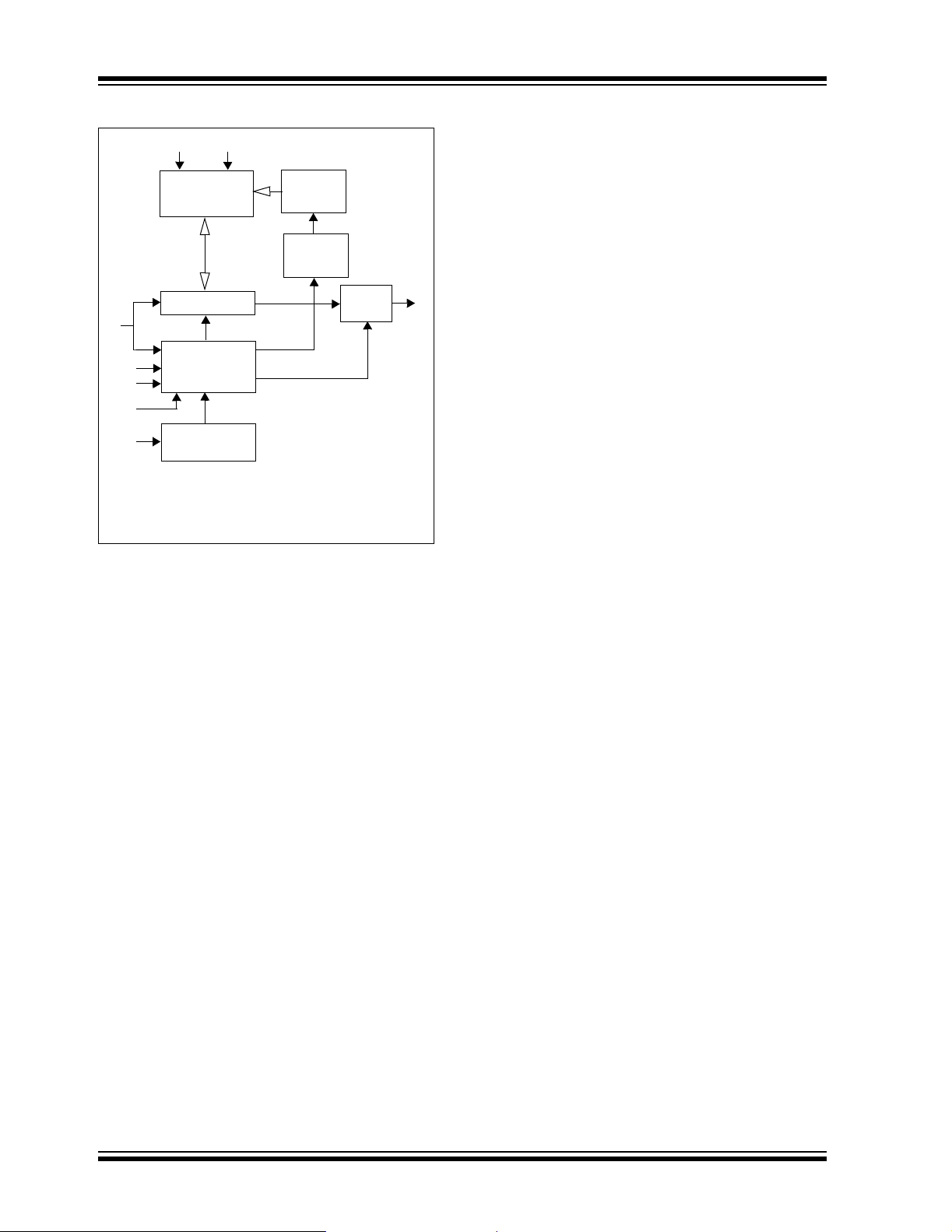
Block Diagram
CC VSS
V
Memory
Array
Data Register
DI
Mode
ORG*
CS
PE*
CLK
*ORG and PE inputs are not available on
A/B devices.
Decode
Logic
Clock
Register
Address
Decoder
Address
Counter
Output
Buffer
DO
DS21797G-page 6 © 2005 Microchip Technology Inc.
Page 7
93AA86A/B/C, 93LC86A/B/C, 93C86A/B/C
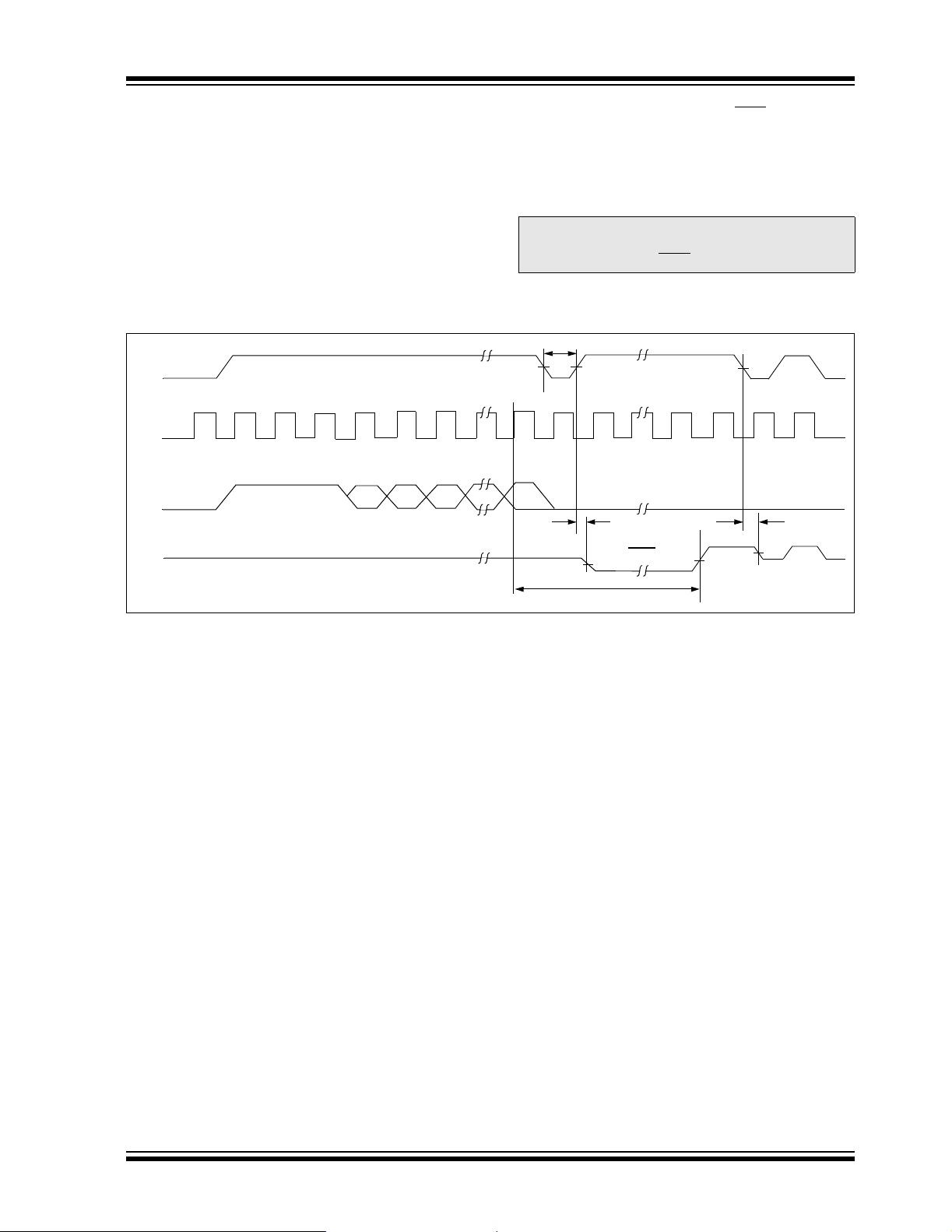
2.4 Erase
The ERASE instruction forces all data bits of the
specified address to the logical ‘1’ state. The rising
edge of CLK before the last address bit initiates the
write cycle.
FIGURE 2-1 : ERASE TIMI NG
CS
CLK
DI
DO
111A
High-Z
N
AN-1 AN-2
The DO pin indicates the Ready/Busy
device if CS is brought high after a minimum of 250 ns
low (TCSL). D O at logical ‘ 0’ indicates that programming
is still in progress. DO at logical ‘1’ indicates that the
register at the specified address has been erased and
the device is ready for another instruction.
Note: After the Erase cycle is complete, issuing
a St art bit and then taki ng CS lo w will c lear
the Ready/Busy s tatus from DO .
T
CSL
Check Status
A0
•••
SV TCZ
T
Busy Ready
status of the
High-Z
WC
T
© 2005 Microchip Technology Inc. DS21797G-page 7
Page 8
93AA86A/B/C, 93LC86A/B/C, 93C86A/B/C
2.5 Erase All (ERAL)
The Erase Al l (ERAL) instruction will erase the entire
memory array to the logical ‘1’ state. The ERAL cycle
is identical to the erase cycle, except for the different
opcode. The ERAL cycle is completely self-timed. The
rising edge of CLK before the last data bit initiates the
write cycle. Clocking of the CLK pin is not necessary
after the device has entered the ERAL cycle.
FIGURE 2-2 : ERAL TIMI N G
CS
CLK
DI
DO
High-Z
100 10x
The DO pin indicates the Ready/Busy
device, if CS is brough t high a fter a minimum of 250 n s
low (TCSL).
Note: After the ERAL command is complete,
issuing a Start bit and then taking CS low
will clear the Ready/Busy status from DO.
VCC must be ≥ 4.5V for proper operation of ERAL.
T
CSL
Check Status
x
•••
SV TCZ
T
Busy Ready
EC
T
status of the
High-Z
DS21797G-page 8 © 2005 Microchip Technology Inc.
Page 9
93AA86A/B/C, 93LC86A/B/C, 93C86A/B/C
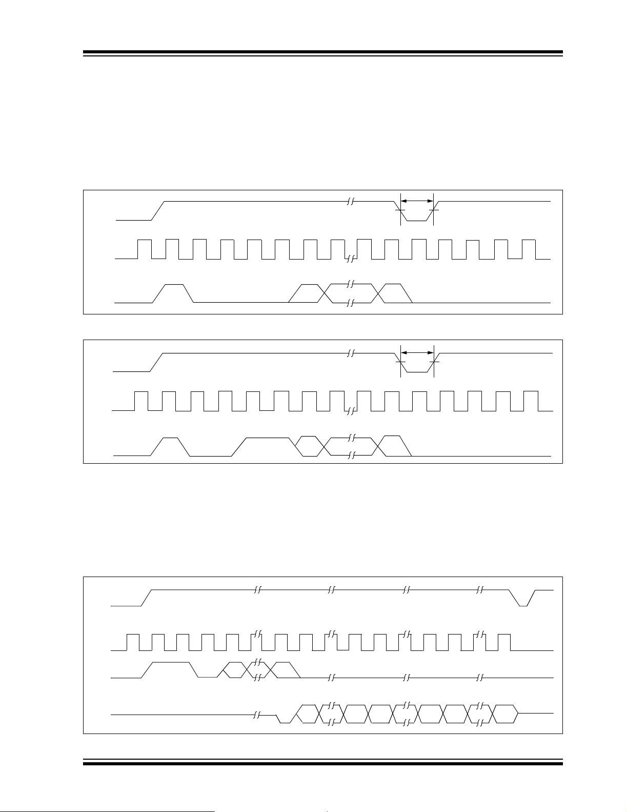
2.6 Erase/Write Disable and Enable
(EWDS/EWEN)
The 93XX86A/B/C powers up in the Erase/Write
Disable (EWDS) state. All programming modes must be
preceded by an Erase/W rite Enable (EWEN) instruc tion.
FIGURE 2-3: EWDS TIMING
CS
CLK
DI
10
FIGURE 2-4: EWEN TIMING
CS
000x
Once the EWEN instruction is executed, programming
remains enabled until an EWDS instruction is executed
or VCC is removed from the device.
To protect against accidental data disturbance, the
EWDS instruction c an be used to di sable all Erase/W ri te
functions and should follow all programming
operations. Execution of a READ instruction is
independent of both the EWEN and EWDS instructions.
CSL
T
•••
x
TCSL
CLK
00 1 1x
DI
1x
2.7 Read
The READ instruction outputs the serial data of the
addressed memory lo cation on the DO pin. A dummy
zero bit precedes the 8-bit (If O RG pin is low or A-V e rsion
devices) or 16-bit (If ORG pin is high or B-version
devices) output string.
FIGURE 2-5 : READ TIMIN G
CS
CLK
A0
DI
110
An
•••
•••
The output data bits will toggle on the rising edge of the
CLK and are stable after the specified time delay (T
PD).
Sequential read is possible when CS is held high. The
memory data will automatically cycle to the next register
and output se qu en ti ally.
DO
© 2005 Microchip Technology Inc. DS21797G-page 9
High-Z
0 Dx
•••
D0 Dx
•••
D0
Dx D0
•••
Page 10

93AA86A/B/C, 93LC86A/B/C, 93C86A/B/C
2.8 Write
The WRITE instruction is followed by 8 bits (If ORG is
low or A-version device s) or 16 b its (If OR G pi n is hig h
or B-version devices) of data which are wr itten into th e
specified address. The self-timed auto-erase and
programming cycle is initiated by the rising edge of CLK
on the last data bit.
FIGURE 2-6 : WRITE TI MI NG
CS
CLK
0
DI
1
1 An
•••
A0 Dx
The DO pin indicates the Ready/Busy
status of the
device, if CS is brough t high a fter a minimum of 250 n s
low (TCSL). D O at logical ‘ 0’ indicates that programming
is still in pro gress. DO at log ical ‘1’ indicates that the
register at the specified address has been written with
the data specified and the device is ready for another
instruction.
Note: The write sequence requires a logic high
signal on the PE pin prior to the rising
edge of the last data bit.
Note: After the Write cy cle is c omplete, issuing a
Start bit and then taking CS low will clear
the Ready/Busy s tatus from DO
TCSL
D0
•••
TSV
TCZ
DO
High-Z
TWC
Busy
Ready
High-Z
DS21797G-page 10 © 2005 Microchip Technology Inc.
Page 11

93AA86A/B/C, 93LC86A/B/C, 93C86A/B/C
2.9 Write All (WRAL)
The Write All (WRAL) instruction will write the entire
memory array with the data specified in the command.
The self-timed auto-erase and programming cycle is
initiated by the rising edge of CLK on the last data bit.
Clocking of the CLK pin is not necessary after the
device has entered the WRAL cycle. The WRAL
command does include an automatic ERAL cycle for
the device. Therefore, the WRAL instruction does not
require an ERAL instructi on, but the chip must b e in th e
EWEN status.
FIGURE 2-7 : WRAL TIMI N G
CS
CLK
The DO pin indicates the Ready/Busy
status of the
device if CS is brought high after a minimum of 250 ns
low (TCSL).
Note: The write sequence requires a logic high
signal on the PE pin prior to the rising
edge of the last data bit.
Note: After the Write All cycle is complete,
issuing a Start bit and then taking CS low
will clear the Ready/Busy
CC must be ≥ 4.5V for proper operation of WRAL.
V
TCSL
status from DO.
DO
DI
1
0
High-Z
01 x
0
•••
x
Dx •••
D0
TSV
Busy
Ready
T
WL
TCZ
High-Z
© 2005 Microchip Technology Inc. DS21797G-page 11
Page 12

93AA86A/B/C, 93LC86A/B/C, 93C86A/B/C
3.0 PIN DESCRIPTIONS
TABLE 3-1: PIN DESCRIPTIONS
SOIC/PDIP/
Name
CS 1 5 Chip Select
CLK 2 4 Serial Clock
DI 3 3 Data In
DO 4 1 Data Out
SS 5 2 Ground
V
ORG 6 — Organization / 93XX86C
PE 7 — Program Enable
CC 8 6 Power Supply
V
MSOP/TSSOP/
DFN
SOT-23 Function
3.1 Chip Select (CS)
A high level sel ects the device; a low lev el deselects
the device and fo rces it into S t andby mo de. Howev er , a
programming cycle wh ic h is al ready in progress will be
completed, regardless of the Chip Select (CS) input
signal. If CS is brou gh t l ow duri ng a p rogram cycle, the
device will go into Standby mode as soon as the
programming cycle is com pleted.
CS must be low for 250 ns minimum (T
consecutive instructions. If CS is low, the internal
control logic is held in a Reset status.
CSL) between
3.2 Serial Clock (CLK)
The Serial Clock is used to synchronize the communication between a master device and the 93XX series
device. Opcodes, address and data bits are clocked in
on the positive edge of C LK. Dat a bit s are also c locke d
out on the positive edge of CLK.
CLK can be stopped anywhere in the transmission
sequence (at high or low level) and can be continued
anytime with respect to clock high time (T
clock low time (T
freedom in preparing opcode, address and data.
CLK is a “don't care” if CS is l ow (devic e desele cted). If
CS is high, but the Start condition has not been
detected (D I = 0), any number of clock cycles can be
received by the device without changing its status (i.e.,
waiting for a Start condition).
CLK cycles are not required during the self-timed write
(i.e., auto erase/write) cycle.
After detection of a Sta rt condition t he specified numb er
of clock cycl es (respectivel y low-to-high tr ansitions of
CLK) must be provided. These clock cycles are
required to clock in all required opcode, address and
data bits b efo re a n in struction is executed. CLK an d DI
then become “don't care” i npu ts waiting for a new Start
condition to be detected.
CKL). This gives the controlling master
CKH) and
3.3 Data In (DI)
Data In (DI) is used to clock in a Start bit, opcode,
address and data, synchronously with the CLK input.
3.4 Data Out (DO)
Data Out (DO) is use d in the Read m ode to outpu t data
synchronously with the CLK input (T
positive edge of CLK).
This pin also provides Ready/Busy
during erase and write cycles. Ready/Busy
information is available on the DO pin if CS is brought
high after being low for minimum Chip Select low time
CSL), and an erase or write operation has been
(T
initiated.
The Status signal is not available on DO if CS is held
low during the entire erase or write cycle. In this case,
DO is in the High-Z mode. If st atus is check ed after th e
erase/write cycle, the data line will be high to indicate
the device is ready.
Note: After a programming cycle is complete,
issuing a Start bit and then taking CS low
will clear the Ready/Busy status from DO.
PD after the
status inf ormation
status
3.5 Organization (ORG)
When the ORG pin i s connected to VCC or Logic HI, th e
(x16) memory organiza tion is sel ected. Whe n the ORG
pin is tied to V
organization is selected. For proper operation, ORG
must be tied to a valid logic level.
93XX86A devices are always x8 organization and
93XX86B devices are always x16 organization.
SS or Logic LO, the (x8) memory
DS21797G-page 12 © 2005 Microchip Technology Inc.
Page 13

93AA86A/B/C, 93LC86A/B/C, 93C86A/B/C
3.6 Program Enable (PE)
This pin allows the user to enable or disable the ability
to write data to the memory array. If the PE pin is tied
CC, the device can be programm ed. If the PE pin is
to V
tied to V
cannot be floated, it must be tied to V
not available on 93XX86A or 93XX86B. On those
devices, programming is always enabled.
SS, programming will be inhibited. This pin
CC or VSS. PE is
© 2005 Microchip Technology Inc. DS21797G-page 13
Page 14

93AA86A/B/C, 93LC86A/B/C, 93C86A/B/C
4.0 PACKAGING INFORMATION
4.1 Package Marking Information
8-Lead MSOP (150 mil)
XXXXXXT
YWWNNN
6-Lead SOT-23
XXNN
8-Lead PDIP
XXXXXXXX
T/XXXNNN
YYWW
8-Lead SOIC
Example:
3L86CI
5281L7
Example:
5EL7
Example:
93LC86C
I/P 1L7
3
e
0528
Example:
SOT23 Marking Codes
Device
93AA86A
93AA86B
93LC86A
93LC86B
93C86A
93C86B
Pb-free topside mark is same; Pb-free
noted only on carton label.
I-temp
5BNN
5LNN
5ENN
5PNN
5HNN
5TNN
E-temp
5FNN
5RNN
5JNN
5UNN
–
–
XXXXXXXT
XXXXYYWW
NNN
8-Lead TSSOP
XXXX
TYWW
NNN
8-Lead 2x3 DFN
XXX
YWW
NN
93LC86CI
SN 0528
3
e
1L7
Example:
L86C
I528
1L7
Example:
3E4
528
L7
DS21797G-page 14 © 2005 Microchip Technology Inc.
Page 15

93AA86A/B/C, 93LC86A/B/C, 93C86A/B/C
l
1st Line Marking Codes
Part Number
93AA86C A86C 3A86CT 3E1 —
93LC86C L86C 3L86CT 3E4 3E5
93C86C C86C 3C86CT 3E7 3E8
Note: T = Temperature grade (I, E)
Legend: XX...X Part number or part number code
Note: For very small packages with no room for the Pb-free JEDEC designator
Note: In the event the full Microchip part num ber can not be ma rked on one line , it wil
TSSOP MSOP
T Temperature (I, E)
Y Year code (last digit of calendar year)
YY Year code (last 2 digits of calendar year)
WW Week code (week of J anuary 1 is week ‘01’)
NNN Alphanumeric traceability code (2 characters for small packages)
Pb-free JEDEC designator for Matte Tin (Sn)
3
e
, the marking will only appear on the outer carton or reel label.
3
e
be carried over to the next line, thus limiting the number of available
characters for customer-specific information.
I Temp. E Temp.
DFN
Note: Please visit www.microchip.com/Pbfree for the latest information on Pb-free conversion.
*Standard OTP marking consists of Microchip part number, year code, week code, and traceability code.
© 2005 Microchip Technology Inc. DS21797G-page 15
Page 16

93AA86A/B/C, 93LC86A/B/C, 93C86A/B/C
8-Lead Plastic Micro Small Outline Package (MS) (MSOP)
E
E1
p
D
B
n 1
2
α
A
c
(F)
β
Units
Dimension Limits
Number of Pins
Pitch
Overall Height
Molded Package Thickness
Standoff
Overall Width
Molded Package Width
Overall Length
Foot Length
Foot Angle
Lead Thickness
Lead Width
Mold Draft Angle Top
Mold Draft Angle Bottom
*Controlling Parameter
Notes:
Dimensions D and E1 do not include mold flash or protrusions. Mold flash or protrusions shall not
exceed .010" (0.254mm) per side.
JEDEC Equivalent: MO-187
Drawing No. C04-111
A2
A1
E1
MIN
n
p
A
E
D
L
φ
c
B
α
β
.026 BSC
.030
.000
.193 TYP.
.118 BSC
.118 BSC
.016 .024
.037 REFFFootprint (Reference)
0° - 8°
.003
.009
5°
5° -
L
INCHES
NOM
.033
.006
.012
φ
A1
MAX NOM
8
--
-
-
.043
.037
.006
.031
.009
.016
15°
15°
MIN
0.75
0.00
0.40
0.08
0.22
MILLIMETERS*
MAX
8
0.65 BSC
--
0.85
-
4.90 BSC
3.00 BSC
3.00 BSC
0.60
0.95 REF
0°
-
-
-
A2
1.10
0.95
0.15
0.80
8°
0.23
0.40
15°5° 15°5° -
DS21797G-page 16 © 2005 Microchip Technology Inc.
Page 17

93AA86A/B/C, 93LC86A/B/C, 93C86A/B/C
6-Lead Plastic Small Outline Transistor (OT) (SOT-23)
E
E1
B
n
c
β
Number of Pins
Pitch
Outside lead pitch (basic)
Molded Package Thickness
Standoff
erall Width
Molded Package Width
Foot Angle
Lead Thickness
Mold Draft Angle Top
Mold Draft Angle Bottom
*Controlling Parameter
Notes:
Dimensions D and E1 do not include mold flash or protrusions. Mold flash or protrusions shall not
exceed .005" (0.127mm) per side.
n
p
p1
A2
A1
E1
φ
c
α
β
p1
D
1
A
φ
NOM
A1
MINMAX
L
MINDimension Limits
α
A2
MILLIMETERSINCHES*Units
NOM
MAX
66
0.95.038
1.90.075
1.451.180.90.057.046.035AOverall Height
1.301.100.90.051.043.035
0.150.080.00.006.003.000
3.002.802.60.118.110.102EOv
1.751.631.50.069.064.059
3.102.952.80.122.116.110DOverall Length
0.550.450.35.022.018.014LFoot Length
10501050
0.200.150.09.008.006.004
0.500.430.35.020.017.014BLead Width
10501050
10501050
JEITA (formerly EIAJ) equivalent: SC-74A
Drawing No. C04-120
© 2005 Microchip Technology Inc. DS21797G-page 17
Page 18

93AA86A/B/C, 93LC86A/B/C, 93C86A/B/C
8-Lead Plastic Dual In-line (P) – 300 mil (PDIP)
E1
D
2
n
E
β
eB
Number of Pins
Pitch
Top to Seating Plane A .140 .155 .170 3.56 3.94 4.32
Molded Package Thickness A2 .115 .130 .145 2.92 3.30 3.68
Base to Seating Plane A1 .015 0.38
Shoulder to Shoulder Width E .300 .313 .325 7.62 7.94 8.26
Molded Package Width E1 .240 .250 .260 6.10 6.35 6.60
Overall Length D .360 .373 .385 9.14 9.46 9.78
Tip to Seating Plane L .125 .130 .135 3.18 3.30 3.43
Lead Thickness
Upper Lead Width B1 .045 .058 .070 1.14 1.46 1.78
Lower Lead Width B .014 .018 .022 0.36 0.46 0.56
Overall Row Spacing § eB .310 .370 .430 7.87 9.40 10.92
Mold Draft Angle Top
Mold Draft Angle Bottom
* Controlling Parameter
§ Significant Characteristic
Notes:
Dimensions D and E1 do not include mold flash or protrusions. Mold flash or protrusions shall not exceed
.010” (0.254mm) per side.
JEDEC Equivalent: MS-001
Drawing No. C04-018
Dimension Limits MIN NOM MAX MIN NOM MAX
1
α
A
c
Units INCHES* MILLIMETERS
n
p
c
α
β
.008 .012 .015 0.20 0.29 0.38
A1
B1
B
88
.100 2.54
51015 51015
51015 51015
A2
L
p
DS21797G-page 18 © 2005 Microchip Technology Inc.
Page 19

93AA86A/B/C, 93LC86A/B/C, 93C86A/B/C
8-Lead Plastic Small Outline (SN) – Narrow, 150 mil (SOIC)
E
E1
p
D
2
B
Number of Pins
Pitch
Standoff §
Foot Angle
Lead Thickness
Mold Draft Angle Top
Mold Draft Angle Bottom
* Controlling Parameter
§ Significant Characteristic
Notes:
Dimensions D and E1 do not include mold flash or protrusions. Mold flash or protrusions shall not exceed
.010” (0.254mm) per side.
JEDEC Equivalent: MS-012
Drawing No. C04-057
n
45°
c
β
n
p
A1
φ
c
α
β
1
h
A
φ
L
048048
A1
MILLIMETERSINCHES*Units
1.27.050
α
A2
MAXNOMMINMAXNOMMINDimension Limits
88
1.751.551.35.069.061.053AOverall Height
1.551.421.32.061.056.052A2Molded Package Thickness
0.250.180.10.010.007.004
6.206.025.79.244.237.228EOverall Width
3.993.913.71.157.154.146E1Molded Package Width
5.004.904.80.197.193.189DOverall Length
0.510.380.25.020.015.010hChamfer Distance
0.760.620.48.030.025.019LFoot Length
0.250.230.20.010.009.008
0.510.420.33.020.017.013BLead Width
1512015120
1512015120
© 2005 Microchip Technology Inc. DS21797G-page 19
Page 20

93AA86A/B/C, 93LC86A/B/C, 93C86A/B/C
8-Lead Plastic Thin Shrink Small Outline (ST) – 4.4 mm (TSSOP)
E
E1
p
D
2
n
B
1
A
c
A1
φ
β
Units
A1
n
p
φ
c
α
β
048048
Number of Pins
Pitch
Standoff §
Foot Angle
Lead Thickne ss
Mold Draft Angle Top
Mold Draft Angle Bottom
* Controlling Parameter
§ Significant Characteristic
Notes:
Dimensions D and E1 do not include mold flash or protrusions. Mold flash or protrusions shall not exceed
.005” (0.127mm) per side.
JEDEC Equivalent: MO-153
Drawing No. C04-086
L
MILLIMETERS*INCHES
0.65.026
α
A2
MAXNOMMINMAXNOMMINDimension Limits
88
1.10.043AOverall Height
0.950.900.85.037.035.033A2Molded Package Thickness
0.150.100.05.006.004.002
6.506.386.25.256.251.246EOverall Width
4.504.404.30.177.173.169E1Molded Package Width
3.103.002.90.122.118.114DMolded Package Length
0.700.600.50.028.024.020LFoot Length
0.200.150.09.008.006.004
0.300.250.19.012.010.007BLead Width
10501050
10501050
DS21797G-page 20 © 2005 Microchip Technology Inc.
Page 21

93AA86A/B/C, 93LC86A/B/C, 93C86A/B/C
8-Lead Plastic Dual Flat No Lead Package (MC) 2x3x0.9 mm Body (DFN) – Saw Singulated
D
K
bp
n
L
E
EXPOSED
METAL
PAD
(
NOTE 2
)
PIN 1
ID INDEX
AREA
NOTE 1
)
(
A3
Number of Pins
Pitch
Standoff
Contact Thickness
Overall Length
Overall Width
Exposed Pad Length
Exposed Pad Width
Contact Length §
Contact-to-Exposed Pad
Contact Width
*
Controlling Parameter
**
Not within JEDEC parameters
§
Significant Characteristic
Notes:
1.
Pin 1 visual index feature may vary, but must be located within the hatched area.
2.
Exposed pad may vary according to die attach paddle size.
3.
Package may have one or more exposed tie bars at ends.
BSC: Basic Dimension. Theoretically exact value shown without tolerances.
See ASME Y14.5M
REF: Reference Dimension, usually without tolerance, for information purposes only.
See ASME Y14.5M
JEDEC Equivalent MO-229 VCED-2
DWG No. C04-123
TOP VIEW
Dimension Limits
§
Units
n
e
A1
A3
D
E
D2
E2
L
K
b.0120.20
DETAIL
ALTERNATE
CONTACT
CONFIGURATION
A
A1
INCHES
MIN
.020 BSC
.031 0.80AOverall Height
.000
.008 REF.
.079 BSC
.118 BSC
.051
.059
.012
.008 – – 0.20 ––
EXPOSED
TIE BAR
(
NOTE 3
NOM
.001
.016 0.40.020 0.30 0.50
.010.008
MAX MIN
8
–
–
2 1
D2
BOTTOM VIEW
)
.039.035
.002 0.00
.069
.075
1.30
1.50
**
**
E2
MILLIMETERS
NOM
0.50 BSC
0.90
0.02 0.05
0.20 REF.
2.00 BSC
3.00 BSC
0.25 0.30
Revised 09-12-05
*
MAX
8
1.00
–
–
1.75
1.90
© 2005 Microchip Technology Inc. DS21797G-page 21
Page 22

93AA86A/B/C, 93LC86A/B/C, 93C86A/B/C
APPENDIX A: REVISION HISTORY
Revision C
Corrections to Section 1.0, Electrical Characteristics.
Section 4.1, 6-Lead SOT-23 package to OT.
Revision D
Corrections to Devi ce Select ion Table, T a ble 1-1 , Table
1-2, Section 2.4, Section 2.5, Section 2.8 and Section
2.9. Added note to Figure 2-7.
Revision E
Added DFN package.
Revision F
Added notes throughout.
Revision G
Revised note in Sections 2.8 and 2.9.
Replaced DFN package drawing.
DS21797G-page 22 © 2005 Microchip Technology Inc.
Page 23

93AA86A/B/C, 93LC86A/B/C, 93C86A/B/C
THE MICROCHIP WEB SITE
Microchip provides onlin e support v ia our W WW site at
www.m ic roc hi p.c om . Thi s web si te i s us ed as a m ean s
to make files and information easily available to
customers. Accessible by using your favorite Internet
browser, the web site contains the following
information:
• Product Support – Data sheets and errata,
application notes and sample programs, design
resources, user’s guides and hardware support
documents, lat est softwa re releases and archived
software
• General Technical Support – Frequently Asked
Questions (FAQ), technical support requests,
online discussion groups, Microchip consultan t
program member listing
• Business of Microchip – Product selector and
ordering guides, latest Microchip press releases,
listing of s eminars and events, listings of
Microchip sales offices, distributors and factory
representatives
CUSTOMER CHANGE NOTIFICATION SERVICE
CUSTOMER SUPPORT
Users of Microchip products can receive assistance
through several channels:
• Distributor or Representative
• Local Sal es Office
• Field Application Engineer (FAE)
• Technical Support
• Development Systems Information Line
Customers should contact their distributor,
representative or field application engineer (FAE) for
support. Local sales offices are also available to help
customers. A listing of sales offices and locations is
included in the back of this document.
T echnic al support is avail able throug h the web si te
at: http://support.microchip.com
Microchip’s customer notification service helps keep
customers current on Microchip products. Subscribers
will receive e-mail notification whenever there are
changes, updates, revisions or errata related to a
specified produ ct family or develo pment tool of inte rest.
To register, access the Microchip web site at
www.microchip.com, click on Customer Change
Notification and follow the registration instructions.
© 2005 Microchip Technology Inc. DS21797G-page 23
Page 24

93AA86A/B/C, 93LC86A/B/C, 93C86A/B/C
READER RESPONSE
It is our intentio n to pro vi de you with the best documentation possible to ens ure suc c es sfu l u se of y ou r M ic roc hip product. If you wish to provid e your c omment s on org anizatio n, clarity, subject matter, a nd ways i n whic h our doc umenta tion
can better serve you, please FAX your comments to the Technical Publications Manager at (480) 792-4150.
Please list the following information, and use this outline to provide us with your comments about this document.
To:
RE: Reader Response
From:
Application (optional):
Would you like a reply? Y N
Device: Literature Number:
Questions:
1. What are the best features of this document?
2. How does this document meet your hardware and software development needs?
3. Do you find the organization of this document easy to follow? If not, why?
Technical Publications Manager
Name
Company
Address
City / State / ZIP / Country
Telephone: (_______) _________ - _________
Total Pages Sent ________
FAX: (______) _________ - _________
DS21797G93AA86A/B/C, 93LC86A/B/C, 93C86A/B/C
4. What additions to the document do you think would enhance the structure and subject?
5. What deletions from the document could be made without affecting the overall usefulness?
6. Is there any incorrect or misleading information (what and where)?
7. How would you improve this document?
DS21797G-page 24 © 2005 Microchip Technology Inc.
Page 25

93AA86A/B/C, 93LC86A/B/C, 93C86A/B/C
PRODUCT IDENTIFICATION SYSTEM
To order or obtain information, e.g., on pricing or delivery, refer to the factory or the listed sales office.
PART NO. X
Device
X
Tape & Reel
Temperature
/XX
Package
Range
Device: 93AA86A: 16K 1.8V Microwire Serial EEPROM (x8)
Tape & Reel: Blank = Standard packaging
93AA86B: 16K 1.8V Microwire Serial EEPROM (x16)
93AA86C: 16K 1.8V Microwire Serial EEPROM w/ORG
93LC86A: 16K 2.5V Microwire Serial EEPROM (x8)
93LC86B: 16K 2.5V Microwire Serial EEPROM (x16)
93LC86C: 16K 2.5V Microwire Serial EEPROM w/ORG
93C86A: 16K 5.0V Microwire Serial EEPROM (x8)
93C86B: 16K 5.0V Microwire Serial EEPROM (x16)
93C86C: 16K 5.0V Microwire Serial EEPROM w/ORG
T=Tape & Reel
X
Lead Finish
Examples:
a) 93AA86C-I/MS: 16K, 2048x8 or 1024x16
Serial EEPROM, MSOP package, 1.8V
b) 93AA86AT-I /OT: 16K, 2048x8 Serial EEPRO M,
SOT-23 package, tape and reel, 1.8V
c) 93AA86CT-I/MS: 16K, 2048x8 or 1024x16
Serial EEPROM, MSOP package, tape and
reel, 1.8V
a) 93LC86C-I/MS: 16K, 2048x8, 1024x1 6 Serial
EEPROM, MSOP package, 2.5V
b) 93LC86BT-I/OT: 16K, 1024x16 Serial
EEPROM, SOT-23 package, tape and reel,
2.5V
a) 93C86C-I/MS: 16K, 2048x8 or 1 024x16 S erial
EEPROM, MSOP package, 5.0V
b) 93C86AT-I/OT: 16K, 2048x8 Serial EEPROM,
SOT-23 package, tape and reel, 5.0V
Temperature Range: I = -40°C to +85°C
Package: MS = Plastic MSOP (Micro Small outline, 8-lead)
Lead Finish: Blank = Pb-free - Matte Tin (see Note 1)
E = -40°C to +125°C
OT = SOT-23, 6-lead (Tape & Reel only)
P = Plastic DIP (300 mil body), 8-lead
SN = Plastic SOIC (150 mil body), 8-lead
ST = TSSOP, 8-lead
MC = 2x3 DFN, 8-lead
G = Pb-free - Matte Tin only
Note 1: Most products manufactured after January 2005 will have a Matte Tin (Pb-free) finish. Most products manufactured
before January 2005 will have a finish of approximately 63% Sn and 37% Pb (Sn/Pb).
Please visit www.microchip.com for the latest information on Pb-free conversion, including conversion date codes.
Sales and Support
Data Sheets
Products supported by a preliminary Data Sheet may have an errata sheet describing minor operational differences
and recommended workarounds. To determine if an errata sheet exists for a particular device, please contact one of
the following:
1. Your local Microchip sales office
2. The Microchip Corporate Literature Center U.S. FAX: (480) 792-7277
3. The Microchip Worldwide Site (www.microchip.com)
Please specify which device, revision of silicon and Data Sheet (include Literature #) you are using.
New Customer Notification System
Register on our web site (www.microchip.com/cn) to receive the most current information on our products.
© 2005 Microchip Technology Inc. DS21797G-page 25
Page 26

93AA86A/B/C, 93LC86A/B/C, 93C86A/B/C
NOTES:
DS21797G-page 26 © 2005 Microchip Technology Inc.
Page 27

Note the following details of the code protection feature on Microchip devices:
• Microchip products meet the specification contained in their particular Microchip Data Sheet.
• Microchip believes that its family of products is one of the most secure families of its kind on the market today, when used in the
intended manner and under normal conditions.
• There are dishonest and possibly illegal methods used to breach the code protection feature. All of these methods, to our
knowledge, require using the Microchip products in a manner outside the operating specifications contained in Microchip’s Data
Sheets. Most likely, the person doing so is engaged in theft of intellectual property.
• Microchip is willing to work with the customer who is concerned about the integrity of their code.
• Neither Microchip nor any other semiconductor manufacturer can guarantee the security of their code. Code protection does not
mean that we are guaranteeing the product as “unbreakable.”
Code protection is constantly evolving. We at Microchip are com mitted to continuously improving the code protect ion f eatures of our
products. Attempts to break Microchip’s code protection feature may be a violation of the Digit al Mill ennium Copyright Act. If such acts
allow unauthorized access to your software or other copyrighted work, you may have a right to sue for relief under that Act.
Information contained in this publication regarding device
applications and the like is provided only for your convenience
and may be superseded by updates. It is your responsibility to
ensure that your application meets with your specifications.
MICROCHIP MAKES NO REPRESENTATIONS OR WARRANTIES OF ANY KIND WHETHER EXPRESS OR IMPLIED,
WRITTEN OR ORAL, STATUTORY OR OTHERWISE,
RELATED TO THE INFORMATION, INCLUDING BUT NOT
LIMITED TO ITS CONDITION, QUALITY, PERFORMANCE,
MERCHANTABILITY OR FITNESS FOR PURPOSE.
Microchip disclaims all liability arising from this information and
its use. Use of M icrochip’s prod ucts as critical components in
life support systems is not authorized except with express
written approval by Microchip. No licenses are conveyed,
implicitly or otherwise, under any Microchip intellectual property
rights.
Trademarks
The Microchip name and logo, the Microchip logo, Accuron,
dsPIC, K
EELOQ, microID, MPLAB, PIC, PICmicro, PICSTART,
PRO MATE, PowerSmart, rfPIC, and SmartShunt are
registered trademarks of Microchip Technology Incorporated
in the U.S.A. and other countries.
AmpLab, FilterLab, Migratable Memory, MXDEV, MXLAB,
PICMASTER, SEEVAL, SmartSensor and The Embedded
Control Solutions Company are registered trademarks of
Microchip Technology Incorporated in the U.S.A.
Analog-for-the-Digital Age, Application Maestro, dsPICDEM,
dsPICDEM.net, dsPICworks, ECAN, ECONOMONITOR,
FanSense, FlexROM, fuzzyLAB, In-Circuit Serial
Programming, ICSP, ICEPIC, Linear Active Thermistor,
MPASM, MPLIB, MPLI NK, MPSIM, PICkit , PICDEM,
PICDEM.net, PICLAB, PICtail, PowerCal, PowerInfo,
PowerMate, PowerTool, Real ICE, rfLAB, rfPICDEM, Select
Mode, Smart Serial, SmartTel, Total Endurance, UNI/O,
WiperLock and Zena are trademarks of Microchip Technology
Incorporated in the U.S.A. and other countries.
SQTP is a service mark of Microchip T echnology Incorporated
in the U.S.A.
All other trademarks mentioned herein are property of their
respective companies.
© 2005, Microchip Technology Incorporated, Printed in the
U.S.A., All Rights Reserved.
Printed on recycled paper.
Microchip received ISO/TS-16949:2002 quality system certification for
its worldwide headquarters, design and wafer fabrication facilities in
Chandler and Tempe, Arizona and Mountain View, California in
October 2003. The Company’s quality system processes and
procedures are for its PICmicro
devices, Serial EEPROMs, microperipherals, nonvolatile memory and
analog products. In addition, Microchip’s quality system for the design
and manufacture of development systems is ISO 9001:2000 certified.
®
8-bit MCUs, KEELOQ
®
code hopping
© 2005 Microchip Technology Inc. DS21797G-page 27
Page 28

WORLDWIDE SALES AND SERVICE
AMERICAS
Corporate Office
2355 West Chandler Blvd.
Chandler, AZ 85224-6199
Tel: 480-792-7200
Fax: 480-792-7277
Technical Support:
http://support.microchip.com
Web Address:
www.microchip.com
Atlanta
Alpharetta, GA
Tel: 770-640-0034
Fax: 770-640-0307
Boston
Westborough, MA
Tel: 774-760-0087
Fax: 774-760-0088
Chicago
Itasca, IL
Tel: 630-285-0071
Fax: 630-285-0075
Dallas
Addison, TX
Tel: 972-818-7423
Fax: 972-818-2924
Detroit
Farmington Hills, MI
Tel: 248-538-2250
Fax: 248-538-2260
Kokomo
Kokomo, IN
Tel: 765-864-8360
Fax: 765-864-8387
Los Angeles
Mission Viejo, CA
Tel: 949-462-9523
Fax: 949-462-9608
San Jose
Mountain View, CA
Tel: 650-215-1444
Fax: 650-961-0286
Toronto
Mississauga, Ontario,
Canada
Tel: 905-673-0699
Fax: 905-673-6509
ASIA/PACIFIC
Australia - Sydney
Tel: 61-2-9868-6733
Fax: 61-2-9868-6755
China - Beijing
Tel: 86-10-8528-2100
Fax: 86-10-8528-2104
China - Chengdu
Tel: 86-28-8676-6200
Fax: 86-28-8676-6599
China - Fuzhou
Tel: 86-591-8750-3506
Fax: 86-591-8750-3521
China - Hong Kong SAR
Tel: 852-2401-1200
Fax: 852-2401-3431
China - Qingdao
Tel: 86-532-8502-7355
Fax: 86-532-8502-7205
China - Shanghai
Tel: 86-21-5407-5533
Fax: 86-21-5407-5066
China - Shenyang
Tel: 86-24-2334-2829
Fax: 86-24-2334-2393
China - Shenzhen
Tel: 86-755-8203-2660
Fax: 86-755-8203-1760
China - Shunde
Tel: 86-757-2839-5507
Fax: 86-757-2839-5571
China - Wuhan
Tel: 86-27-5980-5300
Fax: 86-27-5980-5118
China - Xian
Tel: 86-29-8833-7250
Fax: 86-29-8833-7256
ASIA/PACIFIC
India - Bangalore
Tel: 91-80-2229-0061
Fax: 91-80-2229-0062
India - New Delhi
Tel: 91-11-5160-8631
Fax: 91-11-5160-8632
India - Pune
Tel: 91-20-2566-1512
Fax: 91-20-2566-1513
Japan - Yokohama
Tel: 81-45-471- 6166
Fax: 81-45-471-6122
Korea - Gumi
Tel: 82-54-473-4301
Fax: 82-54-473-4302
Korea - Seoul
Tel: 82-2-554-7200
Fax: 82-2-558-5932 or
82-2-558-5934
Malaysia - Penang
Tel: 60-4-646-8870
Fax: 60-4-646-5086
Philippines - Manila
Tel: 63-2-634-9065
Fax: 63-2-634-9069
Singapore
Tel: 65-6334-8870
Fax: 65-6334-8850
Taiwan - Hsin Chu
Tel: 886-3-572-9526
Fax: 886-3-572-6459
Taiwan - Kaohsiung
Tel: 886-7-536-4818
Fax: 886-7-536-4803
Taiwan - Taipei
Tel: 886-2-2500-6610
Fax: 886-2-2508-0102
Thailand - Bangkok
Tel: 66-2-694-1351
Fax: 66-2-694-1350
EUROPE
Austria - Wels
Tel: 43-7242-2244-399
Fax: 43-7242-2244-393
Denmark - Copenhagen
Tel: 45-4450-2828
Fax: 45-4485-2829
France - Paris
Tel: 33-1-69-53-63-20
Fax: 33-1-69-30-90-79
Germany - Munich
Tel: 49-89-627-144-0
Fax: 49-89-627-144-44
Italy - Milan
Tel: 39-0331-742611
Fax: 39-0331-466781
Netherlands - Drunen
Tel: 31-416-690399
Fax: 31-416-690340
Spain - Madrid
Tel: 34-91-708-08-90
Fax: 34-91-708-08-91
UK - Wokingham
Tel: 44-118-921-5869
Fax: 44-118-921-5820
10/31/05
DS21797G-page 28 © 2005 Microchip Technology Inc.
 Loading...