

Page 1
25AA640/25LC640
64K SPI™ Bus Serial EEPROM
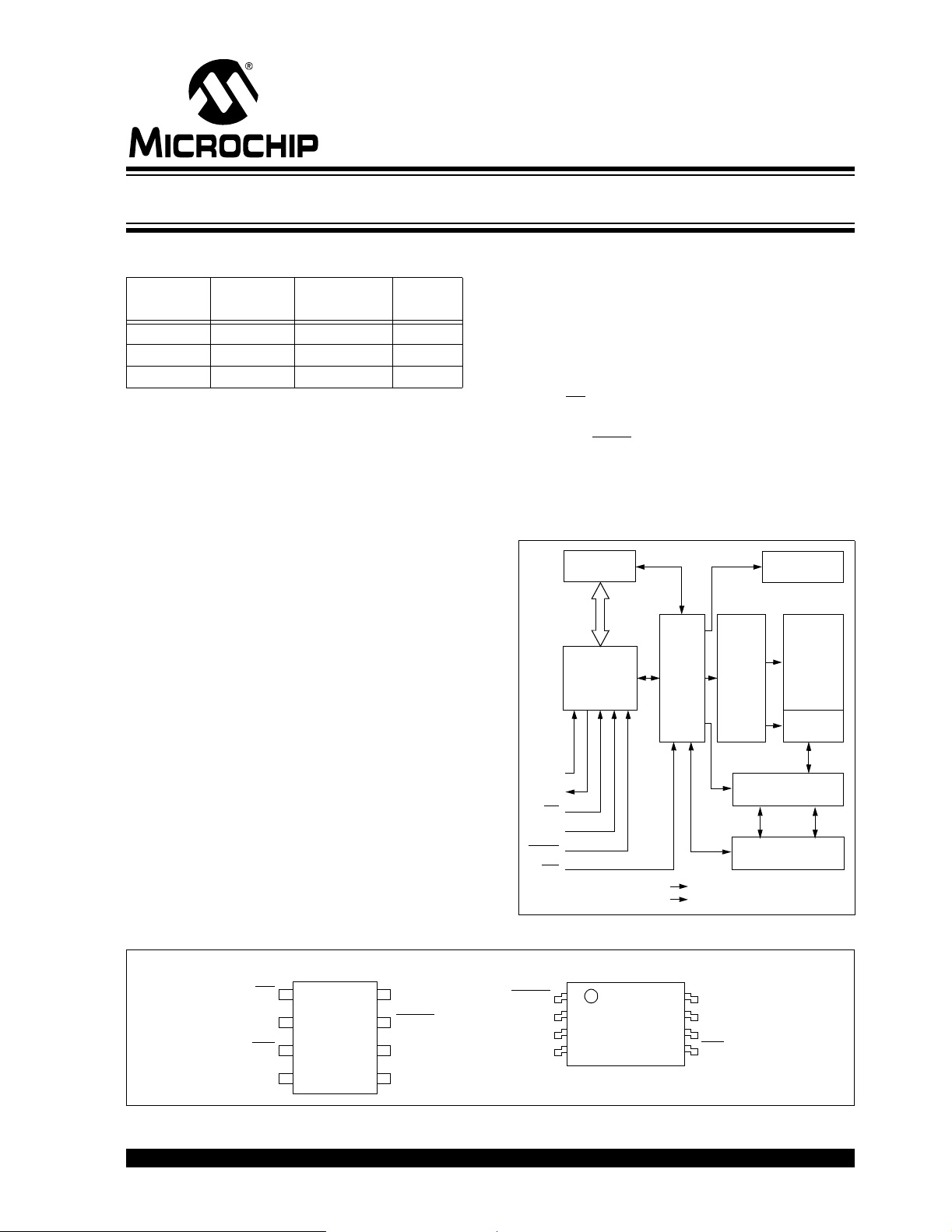
Device Selection Table
Part
Number
25AA640 1.8-5.5V 1 MHz I
25LC640 2.5-5.5V 2 MHz I
25LC640 4.5-5.5V 3/2.5 MHz I, E
VCC
Range
Max Clock
Frequency
Features
• Low-power CMOS technology
- Write current: 3 mA typical
- Read current: 500
- Standby current: 500 nA typical
• 8192 x 8 bit organization
• 32 byte page
• Write cycle time: 5 ms max.
• Self-timed erase and write cycles
• Block write protection
- Protect none, 1/4, 1/2 or all of array
• Built-in write protect ion
- Power on/off data protection circuitry
- Write enable latch
- Write-protect pin
• Sequential read
• High reliability
- Data retention: > 200 years
- ESD protection: > 4000V
• 8-pin PDIP, SOIC and TSSOP packages
• Temperature ranges supported:
- Industrial (I): -40°C to +85°C
- Automotive (E): -40°C to +125°C
µA typical
Temp
Ranges
Description
The Microchip Technology Inc. 25AA640/25LC640
(25XX640
PROM [EEPROM]. The memory is accessed via a
simple Serial Peripheral Interface (SPI) compatible
serial bus. The bus signals required are a clock input
(SCK) plus separate data in (SI) and data out (SO)
lines. Access to the dev ice is contro lled th rough a C hip
Select (CS
Communication to the device can be paused via the
hold pin (HOLD
transitions on its inputs will be ignored, with the
exception of Chip Select, allowing the host to service
higher priority interrupts.
*
) is a 64 Kbit Serial Electrically Erasable
) input.
). While the device is paused,
Block Diagram
SO
CS
SCK
HOLD
WP
SI
Status
Register
I/O Control
Logic
VCC
VSS
Memory
Control
Logic
XDEC
HV Generator
EEPROM
Array
Page
Latches
Y Decoder
Sense Amp.
R/W Control
Package Types
PDIP/SOIC TSSOP
CS
1
25XX640
SO
2
WP
3
VSS
4
*25XX640 is used in this document as a generic part number for the 25AA640/25LC640 devices.
SPI is a registered trademark of Motorola Corporation.
2004 Microchip Technology Inc. DS21223G-page 1
VCC
8
HOLD
7
SCK
6
5
SI
HOLD
VCC
CS
SO
1
2
3
4
25XX640
8
SCK
7
SI
6
V
SS
5
WP
Page 2
25AA640/25LC640
1.0 ELECTRICAL CHARACTERISTICS
Absolute Maximum Ratings
(†)
VCC.............................................................................................................................................................................7.0V
All inputs and outputs w.r.t. V
SS ........................................................................................................ -0.6V to VCC + 1.0V
Storage temperature .................................................................................................................................-65°C to 150°C
Ambient temperature under bias...............................................................................................................-65°C to 125°C
ESD protection on all pins..........................................................................................................................................4 kV
† NOTICE: Stresses above those listed under “Absolute Maximum Ratings” may cause permanent damage to the
device. This is a stres s ratin g only and func tional operati on of the devic e at thos e or any other co nditio ns abov e thos e
indicated in the operational listings of this specification is not implied. Exposure to maximum rating conditions for an
extended period of time may affect device reliability.
TABLE 1-1: DC CHARACTERISTICS
DC CHARACTERISTICS
Param.
No.
D1 V
D2 VIH2 0.7 VCC VCC + 1 V VCC < 2.7V (Note 1)
D3 V
D4 VIL2 -0.3 0.2 VCC VVCC < 2.7V (Note 1)
Sym Characteristics Min Max Units Conditions
IH1 High-level input
voltage
IL1 Low-level input
voltage
D5 VOL Low-level output
voltage
D6 VOH High-level output
Industrial (I): T
Automotive (E): T
2.0 VCC + 1 V VCC ≥ 2.7V (Note 1)
-0.3 0.8 V VCC ≥ 2.7V (Note 1)
—0.4VIOL = 2.1 mA
—0.2VI
VCC - 0.5 — V IOH = -400 µA
voltage
D7 I
D8 ILO Output leakage
LI Input leakage current — ±1 µACS = VCC, VIN = VSS TO VCC
—±1µACS = VCC, VOUT = VSS TO VCC
current
D9 CINT Internal Capacitance
—7pFT
(all inputs and
outputs)
D10 I
CC Read Operating Current —
—
D11 I
CC Write —
—
D12 I
CCS Standby Current —
—
Note 1: This parameter is periodically sampled and not 100% tested.
A = -40°C to +85°C VCC = 1.8V to 5.5V
A = -40°C to +125°C VCC = 4.5V to 5.5V
OL = 1.0 mA, VCC = < 2.5V
A = 25°C, CLK = 1.0 MHz,
CC = 5.0V (Note 1)
V
1
500
mAµAVCC = 5.5V; FCLK = 3.0MHz;
SO = Open
CC = 2.5V; FCLK = 2.0MHz;
V
SO = Open
5
3
5
1
mAmAVCC = 5.5V
CC = 2.5V
V
µAµACS = VCC = 5.5V, Inputs tied to VCC or
SS
V
CS = VCC = 2.5V, Inputs tied to VCC or
V
SS
DS21223G-page 2 2004 Microchip Technology Inc.
Page 3

25AA640/25LC640
TABLE 1-2: AC CHARACTERISTICS
AC CHARACTERISTICS
Param.
No.
1F
Sym Characteristic Min Max Units Conditions
CLK Clock Frequency —
Industrial (I): T
Automotive (E): T
—
—
2T
CSS CS Setup Time 100
250
500
3T
CSH CS Hold Time 150
250
475
4T
5T
CSD CS Disable Time 500 — ns
SU Data Setup Time 30
50
50
6T
HD Data Hold Time 50
100
100
7T
8T
9T
R CLK Rise Time — 2 µs (Note 1)
F CLK Fall Time — 2 µs (Note 1)
HI Clock High Time 150
230
475
10 T
LO Clock Low Time 150
230
475
11 T
12 T
13 T
CLD Clock Delay Time 50 — ns
CLE Clock Enable Time 50 — ns
V Output Valid fro m
Clock Low
—
—
—
14 T
15 T
HO Output Hold Time 0 — ns (Note 1)
DIS Output Disable Time —
—
—
16 T
HS HOLD Setup Time 100
100
200
17 T
HH HOLD Hold Time 100
100
200
18 T
HZ HOLD Low to Outpu t
High-Z
100
150
200
19 T
HV HOLD High to Output
Valid
100
150
200
20 T
WC Internal Write Cycle
—5ms
Time
21 — Endurance 1M — E/W
Note 1: This parameter is periodically sampled and not 100% tested.
2: F
CLK max. = 2.5 MHz for TA > 85°C.
3: This parameter is not tested but established by characterization. For endurance estimates in a specific application,
please consult the Total Endurance™ Model which can be obtained from our web site.
A = -40°C to +85°C VCC = 1.8V to 5.5V
A = -40°C to +125°C VCC = 4.5V to 5.5V
3
2
1
MHz
MHz
MHz
—
—
—
—
—
—
—
—
—
—
—
—
—
—
—
—
—
—
150
230
475
200
250
500
—
—
—
—
—
—
—
—
—
—
—
—
Cycles
CC = 4.5V to 5.5V (Note 2)
V
CC = 2.5V to 5.5V
V
CC = 1.8V to 5.5V
V
ns
VCC = 4.5V to 5.5V
ns
ns
ns
ns
ns
ns
ns
ns
ns
ns
ns
ns
ns
ns
ns
ns
ns
ns
ns
ns
ns
ns
ns
ns
ns
ns
ns
ns
ns
ns
ns
ns
ns
ns
ns
CC = 2.5V to 5.5V
V
CC = 1.8V to 5.5V
V
VCC = 4.5V to 5.5V
CC = 2.5V to 5.5V
V
CC = 1.8V to 5.5V
V
VCC = 4.5V to 5.5V
CC = 2.5V to 5.5V
V
V
CC = 1.8V to 5.5V
VCC = 4.5V to 5.5V
CC = 2.5V to 5.5V
V
V
CC = 1.8V to 5.5V
CC = 4.5V to 5.5V
V
CC = 2.5V to 5.5V
V
CC = 1.8V to 5.5V
V
CC = 4.5V to 5.5V
V
CC = 2.5V to 5.5V
V
CC = 1.8V to 5.5V
V
VCC = 4.5V to 5.5V
V
CC = 2.5V to 5.5V
CC = 1.8V to 5.5V
V
CC = 4.5V to 5.5V (Note 1)
V
CC = 2.5V to 5.5V (Note 1)
V
CC = 1.8V to 5.5V (Note 1)
V
VCC = 4.5V to 5.5V
CC = 2.5V to 5.5V
V
CC = 1.8V to 5.5V
V
VCC = 4.5V to 5.5V
CC = 2.5V to 5.5V
V
CC = 1.8V to 5.5V
V
VCC = 4.5V to 5.5V (Note 1)
CC = 2.5V to 5.5V (Note 1)
V
CC = 1.8V to 5.5V (Note 1)
V
VCC = 4.5V to 5.5V
CC = 2.5V to 5.5V
V
V
CC = 1.8V to 5.5V
(Note 3)
2004 Microchip Technology Inc. DS21223G-page 3
Page 4
25AA640/25LC640
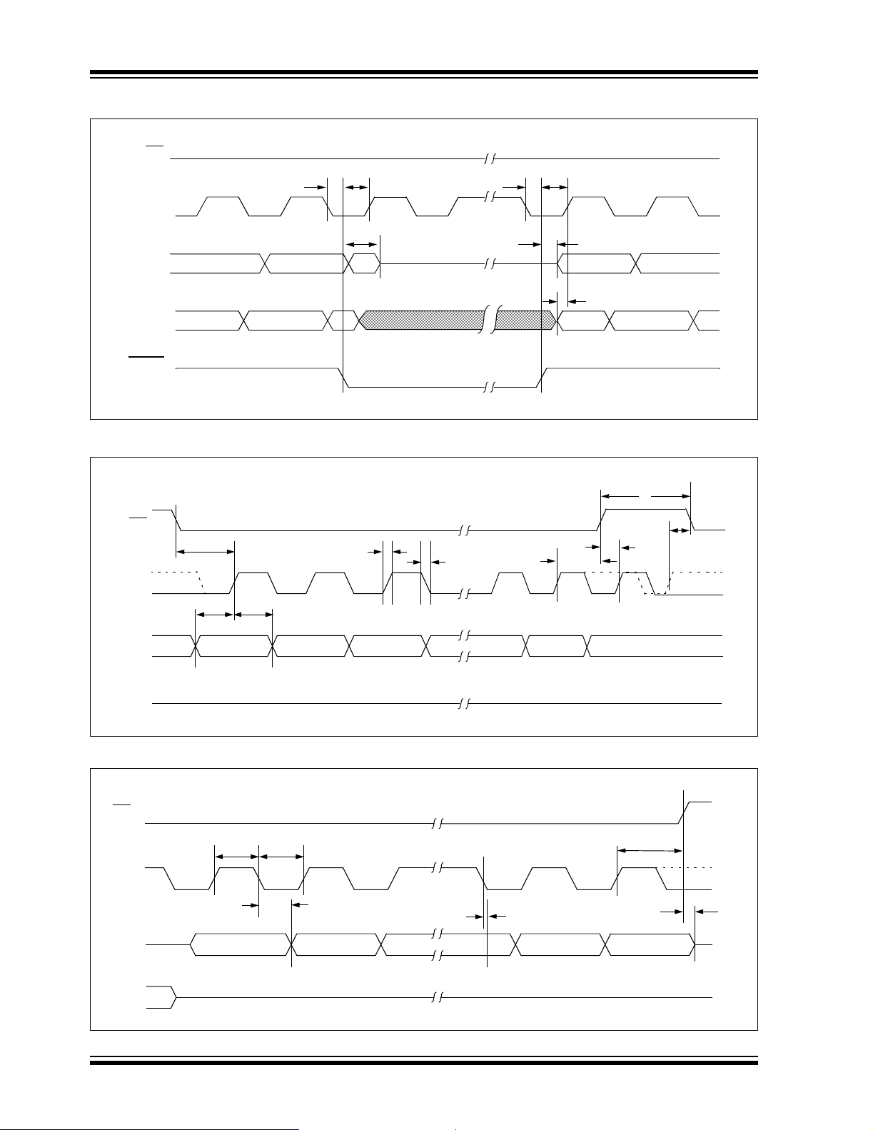
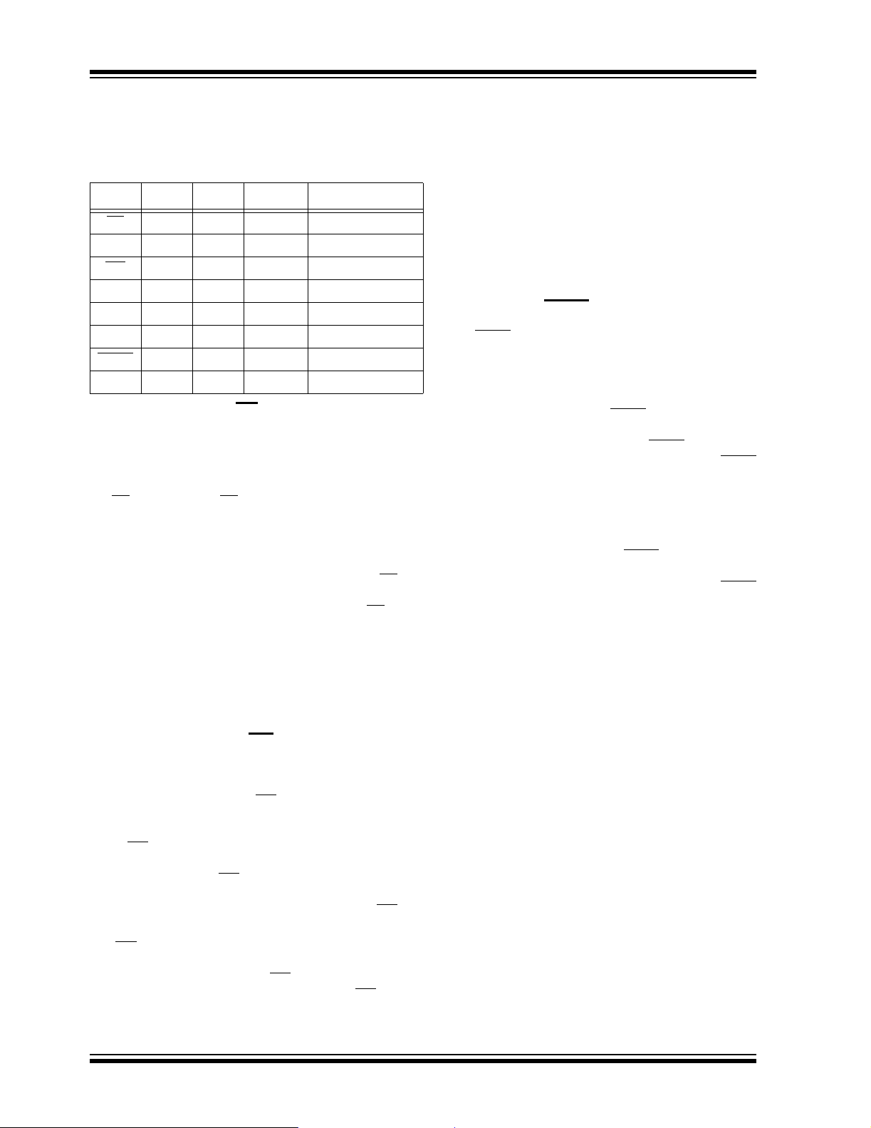
FIGURE 1-1: HOLD TIMING
CS
16 16 17
SCK
SO
n + 2 n + 1 n n - 1
17
High-impedance
1918
n
SI
HOLD
n + 2 n + 1 n
FIGURE 1-2: SERIAL INPUT TIMING
CS
SCK
SI
SO
2
Mode 1,1
Mode 0,0
65
MSB In
High-impedance
7
Don’t Care
8
3
LSB In
5
n
n - 1
4
12
11
FIGURE 1-3: SERIAL OUTPUT TIMING
CS
9
10
SCK
13
SO
SI
DS21223G-page 4 2004 Microchip Technology Inc.
MSB Out
Don’t Care
14
3
Mode 1,1
Mode 0,0
15
LSB Out
Page 5
25AA640/25LC640
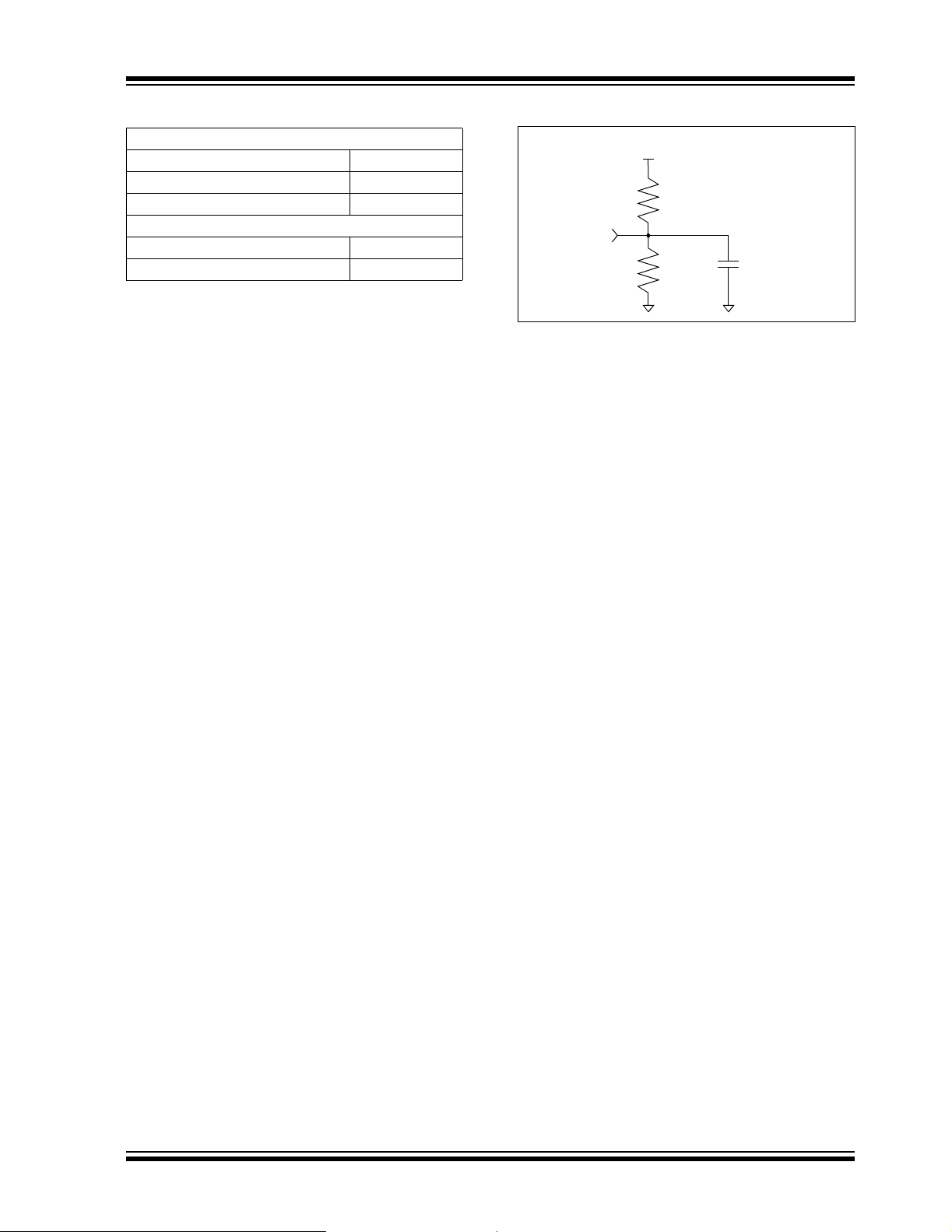
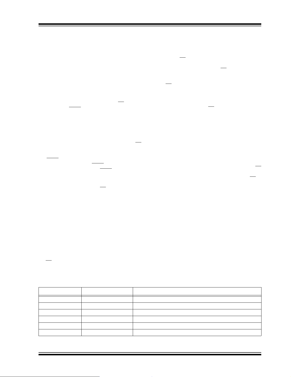
TABLE 1-3: AC TEST CONDITIONS FIGURE 1-4: AC TEST CIRCUIT
AC Waveform:
VLO = 0.2V
HI = VCC – 0.2V (Note 1)
V
VHI = 4.0V (Note 2)
Timing Measurement Reference Lev el
Input 0.5 V
Output 0.5 VCC
Note 1: For VCC ≤ 4.0V
2: For V
CC > 4.0V
CC
SO
VCC
2.25 kΩ
1.8 kΩ
100 pF
2004 Microchip Technology Inc. DS21223G-page 5
Page 6
25AA640/25LC640
2.0 PIN DESCRIPTIONS
The descriptions of the pins are listed in Table 2-1.
TABLE 2-1: PIN FUNCTION TABLE
Name PDIP SOIC TSSOP Description
CS
SO 2 2 4 Serial Data Output
WP
SS 44 6Ground
V
SI 5 5 7 Serial Data Input
SCK 6 6 8 Serial Clock Input
HOLD
V
CC 8 8 2 Supply Voltage
2.1 Chip Select (CS)
A low level on this pin selects the device. A high level
deselects the device and forces it into Standby mode.
However, a programming cycle which is already
initiated or in progress will be completed, regardle ss of
the CS
high during a program cycle, the device will go into
Standby mode when the programming cycle is
complete. When the device is deselected, SO goes to
the high-impedance state, allowing multiple parts to
share the same SPI bus. A low-to-hi gh transition on CS
after a valid write sequence initiates an internal write
cycle. After power-up, a high-to-lo w trans itio n on CS
required prior to any sequence being initiated.
1 1 3 Chip Select Input
3 3 5 Write-Protect Pin
7 7 1 Hold Input
input signal. If CS is brought high, or remains
is
2.4 Serial Input (SI)
The SI pin is used to transfer data into the device. It
receives instructions, addresses, and data. Data is
latched on the rising edge of the serial clock.
2.5 Serial Clock (SCK)
The SCK is used to synchronize the communication
between a master and the 25XX640. Instructions,
addresses, or data present on the SI pin are latched on
the rising edge of t he c lo ck input, while data on the SO
pin is updated after the falling edge of the clock input.
2.6 Hold (HOLD)
The HOLD pin is used to suspend transmission to the
25XX640 while in the middle of a seri al sequ ence wit hout having to retransmit the entire sequence over
again. It must be held high any time this function is not
being used. Once the device is selected and a serial
sequence is underway, the HOLD
low to pause further serial communication without
resetting the serial sequence. The HOLD pin must be
brought low while SCK is low, otherwise the HOLD
function will not be invoked until the next SCK high-tolow transition. The 25XX640 must remain selected
during this sequenc e. The SI, SC K, an d SO p ins a re i n
a high-impedance state during the time the device is
paused and transitions on these p ins will be ignored. To
resume serial communication, HOLD
high while the SCK pin is low, otherwise serial
communication will not resume. Lowering the HOLD
line at any time will tri-state the SO line.
pin may be pulled
must be brought
2.2 Serial Output (SO)
The SO pin is used to transfer data out of the 25XX640.
During a read cycle, data is shifted out on this pin after
the falling edge of the serial clock.
2.3 Write-Protect (WP)
This pin is used in conjunction with the WPEN bit in the
Status register to prohibit writes to the nonvolatile bits
in the Status register. When WP is low and WPEN is
high, writing to the no nvolatil e bits in the Status register
is disabled. All other operations function normally.
When WP
nonvolatile bits in the Status register operate normally.
If the WPEN bit is set, WP low during a Status register
write sequence will disable writing to the Status register. If an internal write cycle has already begun, WP
going low will have no effect on the write.
The WP
the Status register is low. This allows the user to install
the 25XX640 in a system with WP
still be able to write to the Status register. The WP
functions will be enabled when the WPEN bit is set
high.
is high, all functions, including writes to the
pin function is blocked when the WPEN bit in
pin grounded and
pin
DS21223G-page 6 2004 Microchip Technology Inc.
Page 7
25AA640/25LC640
3.0 FUNCTIONAL DESCRIPTION
3.1 Principles Of Operation
The 25XX640 is a 8192 byte Serial EEPROM desi gned
to interface directly with the Serial Peripheral Interface
(SPI) port of many of today’s popular microcontroller
families, including Microchip’s PIC16C6X/7X microcontrollers. It may also interface with microcontrollers
that do not hav e a built-in SPI port by using discrete
I/O lines programmed properly with the software.
The 25XX640 conta ins an 8-bit instr uction regi ster . The
device is accessed via the SI pin, with data being
clocked in on the rising edge of SCK. The CS
be low and the HOLD
operation.
Table 3-1 contains a list of the possible instruction
bytes and format for device operation. All instructions,
addresses, and data are transferred MSB first, LSB
last.
Data is sampled on the fir st rising edge of SCK after CS
goes low. If the clock line is shared with other
peripheral devices on the SPI bus, the user can assert
the HOLD
mode. After releasing the HOLD
resume from the point when the HOLD
input and place the 25XX640 in ‘HOLD’
pin must be high fo r the entire
pin, operation will
3.2 Read Sequence
The device is sele cted by p ulling CS low. The 8-bit read
instruction is transmitted to the 25XX640 followed by
the 16-bit address with the three MSBs of the address
being don’t care bits. After the correct read instruction
and address are sent, the d ata st ored i n the memo ry at
the selected address is shifted out on the SO pin. The
data stored in the memory at the next address can be
read sequentially by continu ing to provide clock pul ses.
The internal address pointer is automatically incremented to the next higher address after each byte of
data is shifted out. When the highest address is
reached (1FFFh), the address counter rolls over to
address 0000h allow in g th e rea d c yc le to b e co nti nue d
indefinitely. The read operation i s term inated by rai sing
pin (Figure 3-1).
the CS
pin must
was asserted.
3.3 Write Sequence
Prior to any attempt to wri t e d at a to the 25XX6 40 arra y
or St atus regis ter, the write enable lat ch mus t be s et by
issuing the WREN instruction (Figure 3-4). This is done
by setting CS
instruction into the 25XX640. After all eight bits of the
instruction are transmitted, the CS
high to set the write enable latch. If the write operation
is initiated immediately after the WREN instruction without CS
to the array because the write enable latch will no t have
been properly set.
Once the write enable latch is set, the user may
proceed by setting the CS
instruction, followed by the address, and then the data
to be written. Up to 32 bytes of data can be sent to the
25XX640 before a write cycle is necessary. The only
restriction is that all of the bytes must reside in the
same page. A page address begins with XXX0 0000
and ends with XXX1 1111. If the internal address
counter reaches XXX1 1111 and the clock continues,
the counter will roll bac k to the first add ress of the p age
and overwrite any da ta in the p age that m ay have bee n
written.
For the data to be actually written to the array, the CS
must be brought high after the Leas t Significant bit (D0)
of the n
brought high at any other time, the write operation will
not be completed. Refer to Figure 3-2 and Figure 3-3
for more detailed illustrations on the byte write
sequence and the page write sequence respectively.
While the write is in progress, the Status register may
be read to check the status of the WPEN, WIP, WEL,
BP1, and BP0 bits (Figure 3-6). A read attempt of a
memory array location will not be possible during a
write cycle. When the write cycle is completed, the
write enable latch is reset.
low and then clocking out the proper
must be brought
being brought high, the data will not be written
low, issuing a WRITE
th
data byte has been clocked in. If CS is
TABLE 3-1: INSTRUCTION SET
Instruction Name Instruction Format Description
READ 0000 0011 Read data from memory array beginning at selected address
WRITE 0000 0010 Write data to memory array beginning at selected address
WREN 0000 0110 Set the write enable latch (enable write operations)
WRDI 0000 0100 Reset the write enable latch (disable write operations)
RDSR 0000 0101 Read Status register
WRSR 0000 0001 Write Status register
2004 Microchip Technology Inc. DS21223G-page 7
Page 8
25AA640/25LC640
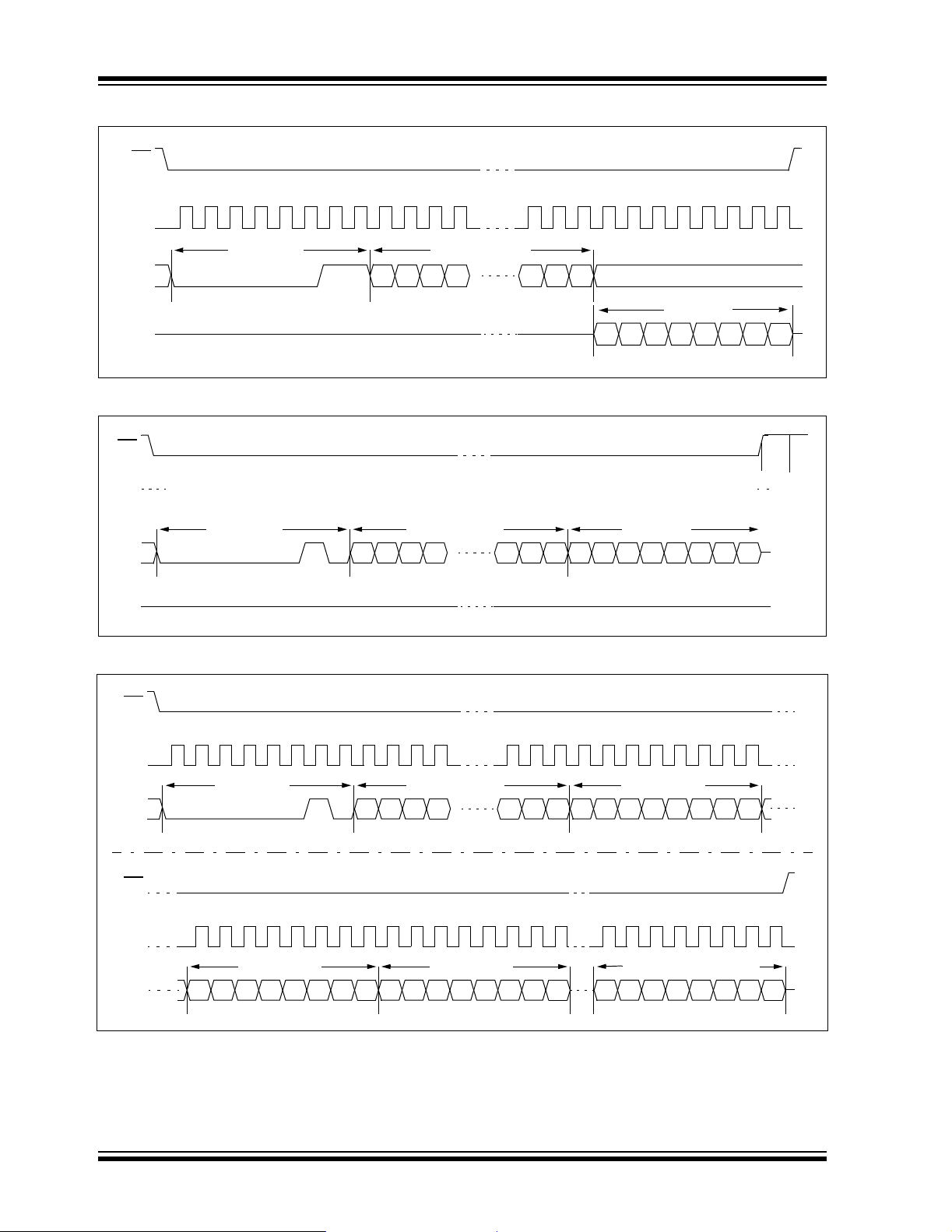
FIGURE 3-1: READ SEQUENCE
CS
0 234567891011 21222324252627282930311
SCK
Instruction 16 Bit Address
SI
0100000 1 15 14 13 12 210
High-impedance
SO
FIGURE 3-2: BYTE WRITE SEQUENCE
CS
Instruction 16 Bit Address Data Byte
SI
SO
0000000 1 15 14 13 12 21076543210
High-impedance
FIGURE 3-3: PAGE WRITE SEQUENCE
CS
8
91011 2122232425262728293031
SCK
SI
0 2345671
Instruction 16 Bit Address Data Byte 1
0000000 1 15 14 13 12
Data Out
76543210
Twc
21076543210
CS
32 34 35 36 37 38 3933
SCK
Data Byte 2
SI
DS21223G-page 8 2004 Microchip Technology Inc.
76543210
41 42 43 46 47
40
Data Byte 3
76543210
44 45
Data Byte n (32 max)
76543210
Page 9
25AA640/25LC640
3.4 Write Enable (WREN) and
Write Disable (WRDI)
The 25XX640 contains a write enable latch. See
Table 3-3 for the Write-Protect Functionality Matrix.
This latch must be set before any write operation w ill be
completed internally. The WREN instruction will set the
latch, and the WRDI will reset the latch.
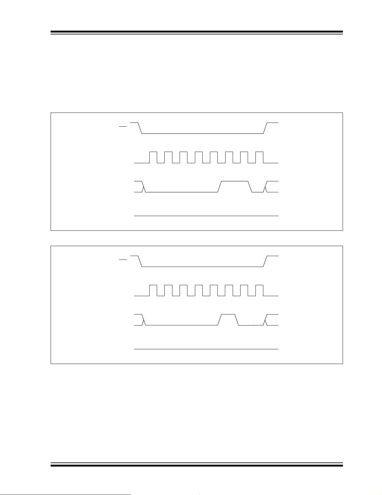
FIGURE 3-4: WRITE ENABLE SEQUENCE
CS
0 2345671
SCK
SI
SO
010000 01
High-impedance
The following is a list of conditions under which the
write enable latch will be reset:
• Power-up
• WRDI instruction successfully executed
• WRSR instruction successfully executed
• WRITE instruction successfully executed
FIGURE 3-5: WRITE DISABLE SEQUENCE
CS
0 2345671
SCK
SI
SO
010000 01
High-impedance
0
2004 Microchip Technology Inc. DS21223G-page 9
Page 10

25AA640/25LC640
3.5 Read Status Register Instruction
(RDSR)
The Read Status Register instruction (RDSR) provides
access to the Status register. The Status register may
be read at any time, even during a write cycle. The
Status register is formatted as follows:
7 654 3 2 1 0
WPEN X X X BP1 BP0 WEL WIP
The Write-In-Process (WIP) bit indicates whether the
25XX640 is busy with a write operation. When set to a
‘1’, a write is in progress, when set to a ‘0’, no write is
in progress. This bit is read-only.
The Wri te Enable Lat ch (WEL) bit indicat es the st atus
of the write enable latch. When set to a ‘1’, the latch
allows writes to the array and Status register, when set
to a ‘0’, the latch proh ibits writes to the array and St atus
register . Th e st a te of this b it ca n alw ays be updat ed via
the WREN or WRDI com m and s regardless of the state
of write protection on the Status register. This bit is
read-only.
The Block Protection (BP0 and BP1) bits indicate
which blocks are currently write-protected. These bits
are set by the user issuing the WRSR instruction. These
bits are nonvolatile.
See Figure 3-6 for RDSR timing sequence.
FIGURE 3-6: READ STATUS REGISTER TIMING SEQUENCE
CS
9101112131415
SCK
SI
0 23456718
Instruction
11000000
SO
High-impedance
Data from Status Register
7654 210
3
DS21223G-page 10 2004 Microchip Technology Inc.
Page 11

25AA640/25LC640
3.6 Write Status Register Instruction
TABLE 3-2: ARRAY PROTECTION
(WRSR)
The Write S t atus Regis ter inst ruction (WRSR) all ows the
user to select one of four levels of protection for the
array by writing to the appropriate bi ts in the S t atus register. The array is divided up into four segments. The
user has the ability to write-protect none, one, two, or
all four of the segment s of the arra y. The partitioning is
controlled as shown in Table 3-2.
The Write-Protect Enable (WPEN) bit is a nonvolatile
bit that is available as an enable bi t for the WP
Write-Protect (WP
(WPEN) bit in the Status register control the programmable hardware write-protect feature. Hardware write
protection is enabled when the WP
WPEN bit is high. Hardw are write protec tion is disa bled
when either the WP pin is high or the WPEN bit is low.
When the chip is hardware write-protected, only writes
to nonvolatile bits in the Status register are disabled.
See T a ble 3-3 for a matrix of functionality on the WPEN
bit.
See Figure 3-7 for WRSR timing sequence.
) pin and the Write-Protect Enable
pin is low and the
pin. The
FIGURE 3-7: WRITE STATUS REGISTER TIMING SEQUENCE
BP1 BP0
00 none
01 upper 1/4
10 upper 1/2
11 all
Array Addresses
Write-Protected
(1800h-1FFFh)
(1000h-1FFFh)
(0000h-1FFFh)
CS
SCK
SI
SO
0 2345671
8
9101112131415
Instruction Data to Status Register
01000000
High-impedance
7654
210
3
2004 Microchip Technology Inc. DS21223G-page 11
Page 12

25AA640/25LC640
3.7 Data Protection
The following protection has been implemented to
prevent in advertent w rites to the array:
• The write enable latch is reset on power-up
• A write enable instruction must be issued to set
the write enable latch
• After a byte write, page write, or Status register
write, the write enable latch is reset
must be set high after the proper number of
•CS
clock cycles to start an internal write cycle
• Access to the array during an intern al write cycl e
is ignored and programming is continued
3.8 Power-On-State
The 25XX640 powers on in the following state:
• The device is in low-power Standby mode
=1)
(CS
• The write enable latch is reset
• SO is in high-impedance state
• A high-to-low transitio n on CS
the active state
.
is required to enter
TABLE 3-3: WRITE-PROTECT FUNCTIONALITY MATRIX
WPEN WP WEL Protected Blocks Unprotected Blocks Status Register
XX 0 Protected Protected Protected
0X 1 Protected Writable Writable
1 Low 1 Protected Writable Protected
X High 1 Protected Writable Writable
DS21223G-page 12 2004 Microchip Technology Inc.
Page 13

4.0 PACKAGING INFORMATION
4.1 Package Marking Information
25AA640/25LC640
8-Lead PDIP (300 mil)
XXXXXXXX
XXXXXNNN
YYWW
8-Lead SOIC (150 mil)
XXXXXXXX
XXXXYYWW
NNN
8-Lead TSSOP
XXXX
YYWW
NNN
Example:
25LC640
/P017
0410
Example:
25LC640
I/SN0410
017
Example:
5LCX
0410
017
Legend: XX...X Customer specific information*
YY Year code (last 2 digits of calendar year)
WW Week code (week of January 1 is week ‘01’)
NNN Alphanumeric traceability code
Note: In the event the full Microchip part numbe r cannot be ma rked on on e line, it will
be carried over to the next line thus limiti ng the number of available characters
for customer specific information.
* Standard marking consists of Microchip part number, year code, week code, traceability code (facility
code, mask rev#, and assembly code). For marking beyond this, certain price adders apply. Please
check with your Microchip Sales Office.
2004 Microchip Technology Inc. DS21223G-page 13
Page 14

25AA640/25LC640
8-Lead Plastic Dual In-line (P) – 300 mil (PDIP)
E1
D
2
n
E
β
eB
Number of Pins
Pitch
Top to Seating Plane A .140 .155 .170 3.56 3.94 4.32
Molded Package Thickness A2 .115 .130 .145 2.92 3.30 3.68
Base to Seating Plane A1 .015 0.38
Shoulder to Shoulder Width E .300 .313 .325 7.62 7.94 8.26
Molded Package Width E1 .240 .250 .260 6.10 6.35 6.60
Overall Length D .360 .373 .385 9.14 9.46 9.78
Tip to Seating Plane L .125 .130 .135 3.18 3.30 3.43
Lead Thickness
Upper Lead Width B1 .045 .058 .070 1.14 1.46 1.78
Lower Lead Width B .014 .018 .022 0.36 0.46 0.56
Overall Row Spacing § eB .310 .370 .430 7.87 9.40 10.92
Mold Draft Angle Top
Mold Draft Angle Bottom
* Controlling Parameter
§ Significant Characteristic
Notes:
Dimensions D and E1 do not include mold flash or protrusions. Mold flash or protrusions shall not exceed
.010” (0.254mm) per side.
JEDEC Equivalent: MS-001
Drawing No. C04-018
Dimension Limits MIN NOM MAX MIN NOM MAX
1
α
A
c
Units INCHES* MILLIMETERS
n
p
c
α
β
.008 .012 .015 0.20 0.29 0.38
A1
B1
B
88
.100 2.54
51015 51015
51015 51015
A2
L
p
DS21223G-page 14 2004 Microchip Technology Inc.
Page 15

8-Lead Plastic Small Outline (SN) – Narrow, 150 mil (SOIC)
E
E1
p
D
2
25AA640/25LC640
B
Number of Pins
Pitch
Standoff §
Foot Angle
Lead Thickness
Mold Draft Angle Top
Mold Draft Angle Bottom
* Controlling Parameter
§ Significant Characteristic
Notes:
Dimensions D and E1 do not include mold flash or protrusions. Mold flash or protrusions shall not exceed
.010” (0.254mm) per side.
JEDEC Equivalent: MS-012
Drawing No. C04-057
n
45°
c
β
n
p
A1
φ
c
α
β
1
h
A
φ
L
048048
A1
MILLIMETERSINCHES*Units
1.27.050
α
A2
MAXNOMMINMAXNOMMINDimension Limits
88
1.751.551.35.069.061.053AOverall Height
1.551.421.32.061.056.052A2Molded Package Thickness
0.250.180.10.010.007.004
6.206.025.79.244.237.228EOverall Width
3.993.913.71.157.154.146E1Molded Package Width
5.004.904.80.197.193.189DOverall Length
0.510.380.25.020.015.010hChamfer Distance
0.760.620.48.030.025.019LFoot Length
0.250.230.20.010.009.008
0.510.420.33.020.017.013BLead Width
1512015120
1512015120
2004 Microchip Technology Inc. DS21223G-page 15
Page 16

25AA640/25LC640
8-Lead Plastic Thin Shrink Small Outline (ST) – 4.4 mm (TSSOP)
Number of Pins
Pitch
Standoff §
Lead Thickne ss
Mold Draft Angle Top
Mold Draft Angle Bottom
A1
MILLIMETERS*INCHESUnits
n
p
c
α
β
MAXNOMMINMAXNOMMINDimension Limits
88
0.65.026
1.10.043AOverall Height
0.950.900.85.037.035.033A2Molded Package Thickness
0.150.100.05.006.004.002
6.506.386.25.256.251.246EOverall Width
4.504.404.30.177.173.169E1Molded Package Width
3.103.002.90.122.118.114DMolded Package Length
0.700.600.50.028.024.020LFoot Length
0.200.150.09.008.006.004
0.300.250.19.012.010.007BLead Width
10501050
10501050
DS21223G-page 16 2004 Microchip Technology Inc.
Page 17

APPENDIX A: REVISION HISTORY
Revision F
Corrections to Section 1.0, Electrical Characteristics.
Revision G
Product ID System, Example C: Corrected part
number, added “Alternate Pinout” and corrected part
number in Header.
Updated Trademark and Sales List pages.
25AA640/25LC640
2004 Microchip Technology Inc. DS21223G-page 17
Page 18

25AA640/25LC640
NOTES:
DS21223G-page 18 2004 Microchip Technology Inc.
Page 19

25AA640/25LC640
ON-LINE SUPPORT
Microchip provides on-line support on the Microchip
World Wide Web site.
The web site is used b y Mic rochip as a me ans to m ake
files and information easily available to customers. To
view the site, the use r must have access to the Intern et
and a web browser, such as Netscape
Internet Explorer. Files are also available for FTP
download from our FTP site.
Connecting to the Microchip Internet
Web Site
The Microchip web site is available at the following
URL:
www.microchip.com
The file transfer site is available by using an FTP
service to connect to:
ftp://ftp.microchip.com
The web site and file transfer site provide a variety of
services. Users may download files for the latest
Development Tools, Data Sheets, Application Notes,
User's Guides, Articles and Sample Programs. A variety of Micr ochip specific bu siness informatio n is also
available, including listings of Microchip sales offices,
distributors and factory representatives. Other data
available for consideration is:
• Latest Microchip Press Releases
• Technical Support Section with Frequently Asked
Questions
• Design Tips
• Device Errata
• Job Postings
• Microchip Consultant Program Member Listing
• Links to other useful web sites related to
Microchip Products
• Conferences for p roducts, D evelopment Systems,
technical information and more
• Listing of seminars and events
®
or Microsoft
SYSTEMS INFORMATION AND UPGRADE HOT LINE
The Systems Information and Upgrade Line provides
system users a listing of the latest versions of all of
Microchip's development systems software products.
®
Plus, this line provides information on how customers
can receive the most c urrent upgrade kit s. The Hot Line
Numbers are:
1-800-755-2345 for U.S. and most of Canada, and
1-480-792-7302 for the rest of the world.
042003
2004 Microchip Technology Inc. DS21223G-page 19
Page 20

25AA640/25LC640
READER RESPONSE
It is our intentio n to pro vi de you with the best documentation possible to ens ure suc c es sfu l u se of y ou r M ic roc hip product. If you wish to provid e your c omment s on org anizatio n, clarity, subject matter , and ways in w hich o ur document atio n
can better serve you, please FAX your comments to the Technical Publications Manager at (480) 792-4150.
Please list the following information, and use this outline to provide us with your comments about this document.
To:
RE: Reader Response
From:
Application (optional):
Would you like a reply? Y N
Device: Literature Number:
Questions:
1. What are the best f eatures of this document?
2. How does this document meet your hardware and software development needs?
3. Do you find the organization of this document easy to follow? If not, why?
Technical Publications Manager
Name
Company
Address
City / State / ZIP / Country
Telephone: (_______) _________ - _________
Total Pages Sent ________
FAX: (______) _________ - _________
DS21223G25AA640/25LC640
4. What additions to the document do you think would enhance the structure and subject?
5. What deletions from the document could be made without affecting the overall usefulness?
6. Is there any incorrect or misleading information (what and where)?
7. How would you improve this document?
DS21223G-page 20 2004 Microchip Technology Inc.
Page 21

25AA640/25LC640
PRODUCT IDENTIFICATION SYSTEM
To order or obtain information, e.g., on pricing or delivery, refer to the factory or the listed sales office.
PART NO. X /XX
Device
Device 25AA640: 64K bit 1.8V SPI Serial EEPROM
Range
25AA640T: 64K bit 1.8V SPI Serial EEPROM
25AA640X: 64K bit 1.8V SPI Serial EEPROM
25AA640XT: 64K bit 1.8V SPI Serial EEPROM
25LC640: 64K bit 2.5V SPI Serial EEPROM
25LC640T: 64K bit 2.5V SPI Serial EEPROM
25LC640X: 64K bit 2.5V SPI Serial EEPROM
25LC640XT: 64K bit 2.5V SPI Serial EEPROM
PackageTemperature
(Tape and Reel)
in alternate pinout (ST only)
in alternate pinout Tape and Reel (ST only)
(Tape and Reel)
in alternate pinout (ST only)
in alternate pinout Tape and Reel (ST only)
Examples:
a) 25AA640-I/SN: Industrial Temp.,
SOIC package
b) 25AA640T-I/SN: Tape and Reel,
Industrial Temp., SOIC package
c) 25AA640X-I/ST: Alternate Pinout
Industrial Temp., TSSOP package
d) 25LC640-I/SN: Industrial Temp.,
SOIC package
e) 25LC640T-I/SN: Tape and Reel,
Industrial Temp., SOIC package
f) 25LC640X-I/ST: Alternate Pinout,
Industrial Temp., TSSOP package
Temperature Range I = -40°C to +85°C
Package P = Plastic DIP (300 mil Body), 8-lead
E= -40°C to +125°C
SN = Plastic SOIC (150 mil Body), 8-lead
ST = Plastic TSSOP (4.4 mm Body), 8-lead
Sales and Support
Data Sheets
Products supported by a preliminary Data Sheet may have an errata sheet describing minor operational differences and recommended workarounds. To determine if an errata sheet exists for a particular device, please contact one of the following:
1. Your local Microchip sales office
2. The Microchip Corporate Literature Center U.S. FAX: (480) 792-7277
3. The Microchip Worldwide Site (www.microchip.com)
Please specify which device, revision of silicon and Data Sheet (include Literature #) you are using.
New Customer Notification System
Register on our web site (www.microchip.com/cn) to receive the most current information on our products.
2004 Microchip Technology Inc. DS21223G-page 21
Page 22

25AA640/25LC640
Page 23

Note the following details of the code protection feature on Microchip devices:
• Microchip products meet the specification contained in their particular Microchip Data Sheet.
• Microchip believes that its family of products is one of the most secure families of its kind on the market today, when used in the
intended manner and under normal conditions.
• There are dishonest and possibly illegal methods used to breach the code protection feature. All of these methods, to our
knowledge, require using the Microchip products in a manner outside the operating specifications contained in Microchip's Data
Sheets. Most likely, the person doing so is engaged in theft of intellectual property.
• Microchip is willing to work with the customer who is concerned about the integrity of their code.
• Neither Microchip nor any other semiconductor manufacturer can guarantee the security of their code. Code protection does not
mean that we are guaranteeing the product as “unbreakable.”
Code protection is constantly evolving. We at Microchip are committed to continuously impro ving the cod e protection features of our
products. Attempts to break Microchip’s code protection feature may be a violation of the Digital Millennium Copyright Act. If such acts
allow unauthorized access to your software or other copyrighted work, you may have a right to sue for relief under that Act.
Information contained in this publication regarding device
applications and the like is intended through suggestion only
and may be superseded by updates. It is your responsibility to
ensure that your application meets with your specifications.
No representation or warranty is given and no liability is
assumed by Microchip Technology Incorporated with respect
to the accuracy or use of such information, or infringement of
patents or other intellectual property rights arising from such
use or otherwise. Use of Microchip’s products as critical
components in life support systems is not authorized except
with express written approval by Microchip. No licenses are
conveyed, implicitly or otherwise, under any intellectual
property rights.
Trademarks
The Microchip name and logo, the Microchip logo, Accuron,
dsPIC, K
EELOQ, MPLAB, PIC, PICmic ro, PI C START,
PRO MATE, PowerSmart and rfPIC are registered
trademarks of Microchip Technology Incorporated in the
U.S.A. and other countries.
AmpLab, FilterLab, microID, MXDEV, MXLAB, PICMASTER,
SEEVAL, SmartShunt and The Embedded Control Solutions
Company are registered trademarks of Microchip Technology
Incorporated in the U.S.A.
Application Maestro, dsPICDEM, dsPICDEM.net,
dsPICworks, ECAN, ECONOMONITOR, FanSense,
FlexROM, fuzzyLAB, In-Circuit Serial Programming, ICSP,
ICEPIC, Migratable Memory, MPASM , MPLIB, MP LIN K,
MPSIM, PICkit, PICDEM, PICDEM.net, PICtail, PowerCal,
PowerInfo, PowerMate, PowerTool, rfLAB, Select Mode,
SmartSensor, SmartTel and Total Endurance are trademarks
of Microchip Technology Incorporated in the U.S.A. and other
countries.
Serialized Quick Turn Programming (SQTP) is a service mark
of Microchip Technology Incorporated in the U.S.A.
All other trademarks mentioned herein are property of their
respective companies.
© 2004, Microchip Technology Incorporated, Printed in the
U.S.A., All Rights Reserved.
Printed on recycled paper.
Microchip re cei v ed I S O/T S - 16 949 : 20 02 qu ality system certif i cat i o n for
its worldwide headquarters, design and wafer fabrication facilities in
Chandler and Tempe, Arizona and Mountain View, California in October
2003. The Com pany’s quality sy stem proces ses and pro cedures are for
its PICmicro
EEPROMs, microperipherals, nonvolatile memory and analog
products. In addition, Microchip’s quality system for the design and
manufacture of development systems is ISO 9001:2000 certified.
®
8-bit MCUs, KEELOQ
®
code hopping devices, Serial
2004 Microchip Technology Inc. DS21223G-page 23
Page 24

WORLDWIDE SALES AND SERVICE
AMERICAS
Corporate Office
2355 West Chandler Blvd.
Chandler, AZ 85224-6199
Tel: 480-792-72 00
Fax: 480-792-7277
Technical Support: 480-792-7627
Web Address: http://www.microchip.com
Atlanta
3780 Mansell Road, Suite 130
Alpharetta, GA 30022
Tel: 770-640- 003 4
Fax: 770-640-0307
Boston
2 Lan Drive, Suite 120
Westford, MA 01886
Tel: 978-692- 384 8
Fax: 978-692-3821
Chicago
333 Pierce Road, Suite 180
Itasca, IL 60143
Tel: 630-285- 007 1
Fax: 630-285-0075
Dallas
4570 Westgrove Drive, Suite 160
Addison, TX 75001
Tel: 972-818- 742 3
Fax: 972-818-2924
Detroit
Tri-Atria Office Building
32255 Northwestern Highway, Suite 190
Farmington Hills, MI 48334
Tel: 248-538- 225 0
Fax: 248-538-2260
Kokomo
2767 S. Albright Road
Kokomo, IN 46902
Tel: 765-864- 836 0
Fax: 765-864-8387
Los Angeles
18201 Von Karman, Suite 1090
Irvine, CA 92612
Tel: 949-263- 188 8
Fax: 949-263-1338
San Jose
1300 Terra Bella Avenue
Mountain View, CA 94043
Tel: 650-215- 144 4
Fax: 650-961-0286
Toronto
6285 Northam Drive, Suite 108
Mississauga, Ontario L4V 1X5, Cana da
Tel: 905-673- 069 9
Fax: 905-673-6509
ASIA/PACIFIC
Australia
Suite 22, 41 Rawson Street
Epping 2121, NSW
Australia
Tel: 61-2-986 8-6 73 3
Fax: 61-2-9868-6755
China - Beijing
Unit 706B
Wan Tai Bei Hai Bldg.
No. 6 Chaoyangmen Bei Str.
Beijing, 100027, China
Tel: 86-10-85 282 10 0
Fax: 86-10-85282104
China - Chengdu
Rm. 2401-2402, 24th Floor,
Ming Xing Financial Tower
No. 88 TIDU Street
Chengdu 610016, China
Tel: 86-28-86 766 20 0
Fax: 86-28-86766599
China - Fuzhou
Unit 28F, World Trade Plaza
No. 71 Wusi Road
Fuzhou 350001, China
Tel: 86-591-7 503 50 6
Fax: 86-591-7503521
China - Hong Kong SAR
Unit 901-6, Tower 2, Metroplaza
223 Hing Fong Road
Kwai Fong, N.T., Hong Kong
Tel: 852-2401 -12 00
Fax: 852-2401-3431
China - Shanghai
Room 701, Bldg. B
Far East International Plaza
No. 317 Xian Xia Road
Shanghai, 200051
Tel: 86-21-62 75- 57 00
Fax: 86-21-6275-5060
China - Shenzhen
Rm. 1812, 18/F, Building A, United Plaza
No. 5022 Binhe Road, Futian District
Shenzhen 518033, China
Tel: 86-755-8 290 13 80
Fax: 86-755-8295-1393
China - Shunde
Room 401, Hongjian Building, No. 2
Fengxiangnan Road, Ronggui Town, Shunde
District, Foshan City, Guangdong 528303, China
Tel: 86-757-28395507 Fax: 86-757-28395571
China - Qingdao
Rm. B505A, Fullhope Plaza,
No. 12 Hong Kong Central Rd.
Qingdao 266071, China
Tel: 86-532-5027355 Fax: 86-532-5027205
India
Divyasree Chambers
1 Floor, Wing A (A3/A4)
No. 11, O’Shaugnessey Road
Bangalore, 560 025, India
Tel: 91-80-22 290 06 1 Fax: 91- 80 -22 29 006 2
Japan
Benex S-1 6F
3-18-20, Shinyokohama
Kohoku-Ku, Yokohama-shi
Kanagawa, 222-0033, Japan
Tel: 81-45-47 1- 616 6 Fax: 81-4 5-4 71 -6122
Korea
168-1, Youngbo Bldg. 3 Floor
Samsung-Dong, Kangnam-Ku
Seoul, Korea 135-882
Tel: 82-2-554-7200 Fax: 82-2-558-5932 or
82-2-558-5934
Singapore
200 Middle Road
#07-02 Prime Centre
Singapore, 188980
Tel: 65-6334-8870 Fax: 65-6334-8850
Taiwan
Kaohsiung Branch
30F - 1 No. 8
Min Chuan 2nd Road
Kaohsiung 806, Taiwan
Tel: 886-7-536-4818
Fax: 886-7-536-4803
Taiwan
Taiwan Branch
11F-3, No. 207
Tung Hua North Road
Taipei, 105, Taiwan
Tel: 886-2-2717-7175 Fax: 886-2-2545-0139
EUROPE
Austria
Durisolstrasse 2
A-4600 Wels
Austria
Tel: 43-7242-2244-399
Fax: 43-7242-2244-393
Denmark
Regus Business Centre
Lautrup hoj 1-3
Ballerup DK-2750 Denmark
Tel: 45-4420-9895 Fax: 45-4420-9910
France
Parc d’Activite du Moulin de Massy
43 Rue du Saule Trapu
Batiment A - ler Etage
91300 Massy, France
Tel: 33-1-69-53-63-20
Fax: 33-1-69-30-90-79
Germany
Steinheilstrasse 10
D-85737 Ismaning, Germany
Tel: 49-89-627-144-0
Fax: 49-89-627-144-44
Italy
Via Quasimodo, 12
20025 Legnano (MI)
Milan, Italy
Tel: 39-0331-742611
Fax: 39-0331-466781
Netherlands
P. A. De Biesbosch 14
NL-5152 SC Drunen, Netherlands
Tel: 31-416-690399
Fax: 31-416-690340
United Kingdom
505 Eskdale Road
Winnersh Triangle
Wokingham
Berkshir e, England RG41 5T U
Tel: 44-118-921-5869
Fax: 44-118-921-5820
02/17/04
DS21223G-page 24 2004 Microchip Technology Inc.
 Loading...