

24AA32A/24LC32A
)
32K I2C™ Serial EEPROM
Device Selection Table
Part
Number
24AA32A 1.8-5.5 400kHz
24LC32A 2.5-5.5 400 kHz I, E
Note 1: 100 kHz for VCC <2.5V
VCC
Range
Max Clock
Frequency
(1)
Temp
Ranges
I
Features
• Single supply with operation down to 1.8V
• Low-power CMOS technology
- 1 mA active current typical
-1µA standby current (max.) (I-temp)
• Organized as 4 blocks of 8K bits (32K bit)
• 2-wire serial interface bus, I
• Cascadable for up to eight devices
• Schmitt Trigger inputs for noise suppression
• Output slope control to eliminate ground bounce
• 100 kHz (<2.5V) and 400 kHz (≥2.5V)
compatibility
• Self-timed write cycle (including auto-erase)
• Page write buffer for up to 32 bytes
• 2 ms typical write cycle time for page write
• Hardware write-protect for entire memory
• Can be operated as a serial ROM
• Factory programming (QTP) available
• ESD protection > 4,000V
• 1,000,000 erase/write cycles
• Data retention > 200 years
• 8-lead PDIP, SOIC, TSSOP and MSOP packages
• Standard and Pb-free finishes available
• Available temperature ranges:
- Industrial (I): -40°C to +85°C
- Automotive (E): -40°C to +125°C
2
C™ compatible
Description
The Microchip Technology Inc. 24AA32A/24LC32A
(24XX32A*) is a 32 Kbit Electrically Erasable PROM.
The device is organized as four blocks of 8K x 8-bit
memory with a 2-wire serial interface. Low-voltage
design permits operation down to 1.8V, with standby
and active currents of only 1 µA and 1 mA,
respectively. It has been developed for advanced, lowpower applications such as personal communications
or data acquisit ion. The 24XX32A also has a page wri te
capability for up to 32 bytes of dat a. Function al address
lines allow up to eight devices on the same bus, for up
to 256 Kbits address space. The 24XX32A is available
in the standard 8-pin PDIP, surface mount SOIC,
TSSOP and MSOP packages.
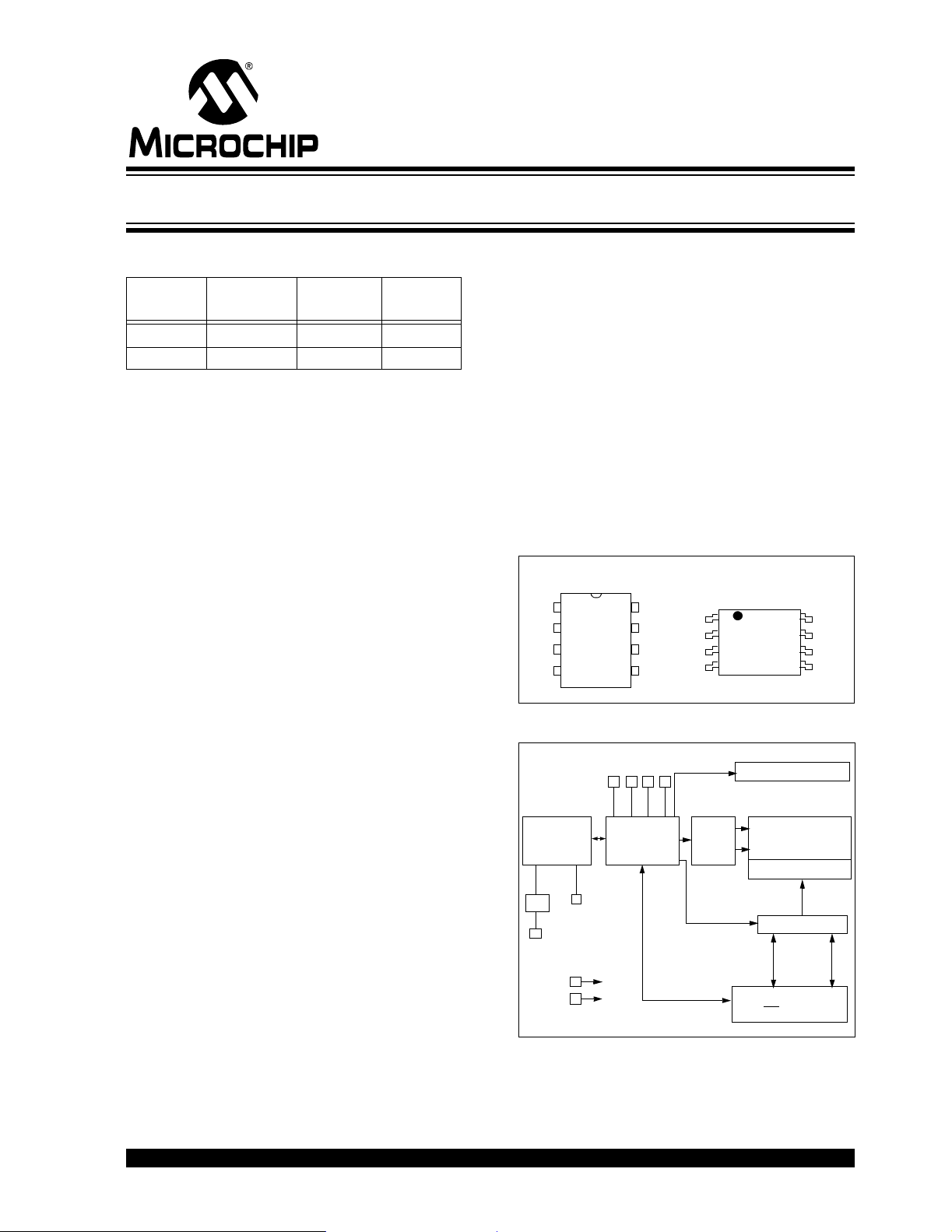
Package Types
PDIP/SOIC/TSSOP/MSOP
A0
A1
A2
Vss
1
2
3
4
24XX32
8
Vcc
7
WP
6
SCL
5
SDA
ROTATED TSSOP
(24AA32AX/24LC32AX
24XX32X
WP
Vcc
A0
A1
1
2
3
4
8
7
6
5
SCL
SDA
Vss
A2
Block Diagram
A0
Control
Logic
I/O
SDA
I/O
A1WPA2
Memory
Control
Logic
SCL
XDEC
HV Generator
EEPROM
Array
Page Latches
YDEC
Vcc
SS
V
*24XX32A is used in this document as a generic part number for the 24AA32A/24LC32A devices.
2003 Microchip Technology Inc. DS21713D-page 1
Sense Amp.
R/W Control
24AA32A/24LC32A
1.0 ELECTRICAL CHARACTERISTICS
Absolute Maximum Ratings
(†)
VCC.............................................................................................................................................................................6.5V
All inputs and outputs w.r.t. V
SS ......................................................................................................... -0.3V to VCC +1.0V
Storage temperature ...............................................................................................................................-65°C to +150°C
Ambient temperature with power applied................................................................................................-65°C to +125°C
ESD protection on all pins ......................................................................................................................................................≥ 4kV
† NOTICE: Stresses above those listed under “Absolute Maximum Ratings” may cause permanent damage to
the device. This is a stress rating only and functional operation of the device at those or any other conditions
above those indica ted in the opera tional li stings of this sp ecification is not i mplied. Ex posure to maximum rating
conditions for extended periods may affect device reliability.
TABLE 1-1: DC CHARACTERISTICS
CC = +1.8V to +5.5V
V
DC CHARACTERISTICS
Param.
No.
D1 V
Symbol Characteristic Min Typ Max Units Conditions
IH WP, SCL and SDA pins — ————
D2 — High-level input voltage 0.7 VCC ——V—
D3 VIL Low-level input voltage — — 0.3 VCC V—
D4 V
HYS Hysteresis of Schmitt
Trigger inputs
D5 V
D6 I
OL Low-level output voltage — — 0.40 V IOL = 3.0 mA, VCC = 2.5V
LI Input leakage current ——±1µAVIN =.1V to VCC
D7 ILO Output leakage current ——±1µAVOUT =.1V to VCC
D8 CIN,
C
OUT
Pin capacitance
(all inputs/outpu t s)
D9 ICC write Operating current —0.13mAVCC = 5.5V, SCL = 400 kHz
D10 ICC read — 0.05 1 mA —
D11 I
CCS Standby current —
Note 1: This parameter is periodically sampled and not 100% tested.
2: Typical measurements taken at room temperature.
Industrial (I): T
Automotive (E): T
A = -40°C to +85°C
A = -40°C to +125°C
0.05 VCC ——V(Note 1)
——10pFVCC = 5.0V (Note 1)
T
A = 25°C, FCLK = 1 MHz
—
0.01
—
1
5
µAµAIndustrial
Automotive
SDA = SCL = V
WP = VSS
CC
DS21713D-page 2 2003 Microchip Technology Inc.
24AA32A/24LC32A
TABLE 1-2: AC CHARACTERISTICS
CC = +1.8V to +5.5V
V
AC CHARACTERISTICS
Param.
No.
1F
Symbol Characteristic Min Max Units Conditions
CLK Clock frequency —
2 THIGH Clock high time 600
3TLOW Clock low time 1300
4T
R SDA and SCL rise time
(Note 1)
5TF SDA and SCL fall time — 300 ns (Note 1)
6T
HD:STA Start condition hold time 600
7TSU:STA Start condition setup time 600
8THD:DAT Data input hold time 0 — ns (Note 2)
9TSU:DAT Data input setup time 100
10 TSU:STO Stop condition setup time 600
11 T
AA Output valid from clock
(Note 2)
12 TBUF Bus free time: Time the bus
must be free before a new
transmissi on can start
13 T
OF Output fall time from VIH
minimum to V
IL maximum
14 TSP Input filter spike suppression
(SDA and SCL pins)
15 T
WC Write cycle time (byte or
page)
16 — Endurance 1M — cycles 25°C, (Note 4)
Note 1: Not 100% tested. C
B = total capacitance of one bus line in pF.
2: As a transmitter, the device must provide an internal minimum delay time to bridge the undefined region
(minimum 300 ns) of the falling edge of SCL to avoid unintended generation of Start or Stop conditions.
3: The combined T
SP and VHYS specificat io ns are due to new Schm it t Trigger inputs which provide improved
noise spike suppression. This eliminates the need for a
4: This parameter is not tested but ensured by character ization. For enduranc e estimates in a specific
application, please consult the Total Endurance™ Model which can be obtained on Microchip’s web site:
www.microchip.com.
Industrial (I): T
Automotive (E): T
—
4000
4700
—
—
4000
4700
250
4000
—
—
1300
4700
20+0.1C
B
—
A = -40°C to +85°C
A = -40°C to +125°C
400
kHz 2.5V ≤ VCC ≤ 5.5V
100
—
ns 2.5V ≤ VCC ≤ 5.5V
—
—
ns 2.5V ≤ VCC ≤ 5.5V
—
300
ns 2.5V ≤ VCC ≤ 5.5V
1000
—
ns 2.5V ≤ VCC ≤ 5.5V
—
—
ns 2.5V ≤ VCC ≤ 5.5V
—
—
ns 2.5V ≤ VCC ≤ 5.5V
—
—
ns 2.5V ≤ VCC ≤ 5.5V
—
900
ns 2.5V ≤ VCC ≤ 5.5V
3500
—
ns 2.5V ≤ VCC ≤ 5.5V
—
250
ns 2.5V ≤ V
250
1.8V ≤ V
1.8V ≤ V
1.8V ≤ V
1.8V ≤ V
1.8V ≤ V
1.8V ≤ V
1.8V ≤ V
1.8V ≤ V
1.8V ≤ V
1.8V ≤ V
1.8V ≤ V
—50ns(Notes 1 and 3)
—5ms—
TI specification for standard operation.
CC < 2.5V (24AA32A)
CC < 2.5V (24AA32A)
CC < 2.5V (24AA32A)
CC < 2.5V (24AA32A)
CC < 2.5V (24AA32A)
CC < 2.5V (24AA32A)
CC < 2.5V (24AA32A)
CC < 2.5V (24AA32A)
CC < 2.5V (24AA32A)
CC < 2.5V (24AA32A)
CC ≤ 5.5V
CC < 2.5V (24AA32A)
2003 Microchip Technology Inc. DS21713D-page 3
24AA32A/24LC32A
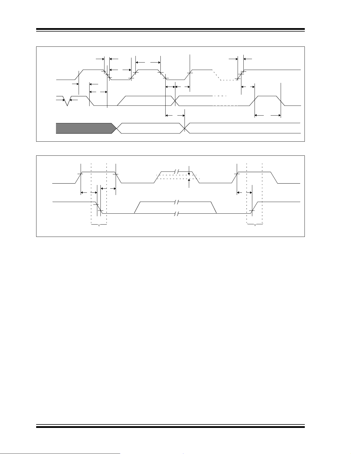
FIGURE 1-1: BUS TIMING DATA
SCL
SDA
IN
SDA
OUT
5
3
7
6
14
2
FIGURE 1-2: BUS TIMING START/STOP
SCL
7
SDA
6
4
8
9
11
D4
10
12
10
Start Stop
DS21713D-page 4 2003 Microchip Technology Inc.
24AA32A/24LC32A
)
2.0 FUNCTIONAL DESCRIPTION
The 24XX32A supports a bidirectional, 2-wire bus and
data transmission protocol. A device that sends data
onto the bus i s defined as t ransmitter, while a de vice
receiving data is defined as a receiver. The bus has to
be controlled by a master device which generates the
serial clock (SCL), controls the bus access and generates the Start and Stop conditions, while the 24XX32A
works as slave. Both master and slave can operate as
transmitter or receiver, but the master device determines which mode is activ ated.
3.0 BUS CHARACTERISTICS
The following bus protocol has been defined:
• Data transfer may be initiated only when the bus
is not busy.
• During data transfer, the data line must remain
stable wheneve r the c lock lin e is high . Changes i n
the data line while the clock line is high will be
interpreted as a Start or Stop condition.
Accordingly, the following bus conditions have been
defined (Figure 3-1).
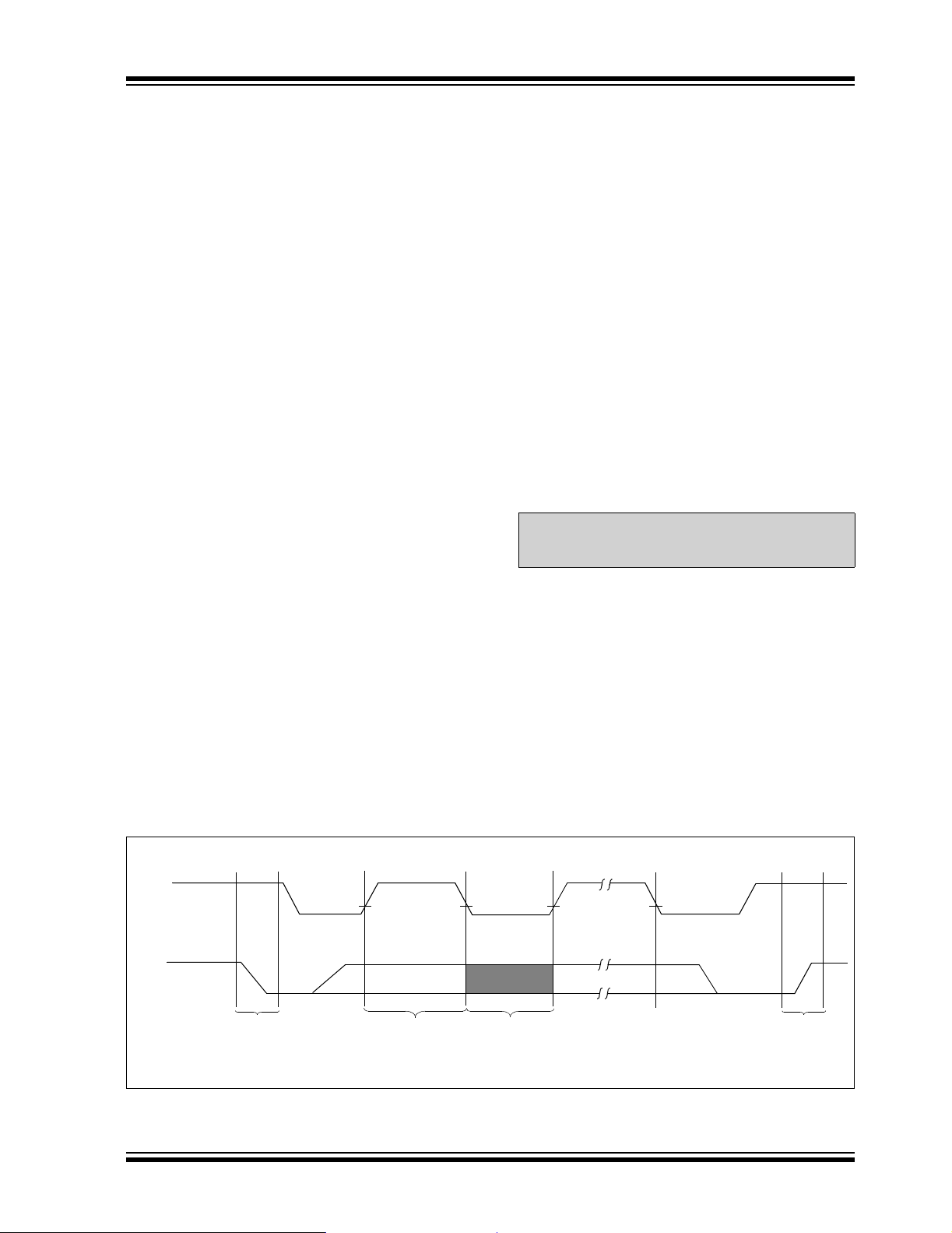
3.1 Bus not Busy (A)
Both data and clock lines remain high.
3.2 Start Data Transfer (B)
A high-to-low transition of the SDA line while the clock
(SCL) is high determines a Start condition. All commands must be preceded by a Start condition.
3.3 Stop Data Transf er (C)
A low-to-high transition of the SDA line while the clock
(SCL) is high determines a Stop condition. All operations must be ended with a Stop condition.
3.4 Data Valid (D)
The state of the data line represents valid data when,
after a Start condition, the data line is stable for the
duration of the high period of the clock signal.
The data on the line must be changed during the low
period of the clock signal. There is one clock pulse per
bit of data.
Each data transfer is initiated with a S tart condition and
terminated with a Stop condition. The number of data
bytes transferred between Start and Stop conditions is
determined by the master device and is, theoretically
unlimited, (althoug h only the la st thirty two by tes will be
stored when doing a write operation). When an overwrite does occur it will replace data in a first-in first-out
(FIFO) fashion.
3.5 Acknowledge
Each receiving device, when addressed, is obliged to
generate an acknowledge after the reception of each
byte. The ma ster devi ce m ust gener at e an ex tr a cloc k
pulse which is associated with this Acknowledge bit.
Note: The 24XX32A does not generate any
Acknowledge bits if an internal
programming cycle is in progress.
The device that acknowledges, has to pull down the
SDA line during the Acknowl edge cloc k pulse in s uch a
way that the SDA line is stable low during the high
period of the acknowledge related clock pulse. Of
course, setup and hold times must be taken into
account. During reads, a master must signal an end of
data to the sla ve by no t gene rating a n Ack nowl edge b it
on the last byte that has be en c loc ke d ou t of th e sl av e.
In this case, the slave (24XX32A) will leave the data
line high to enable the master to generate the Stop
condition.
FIGURE 3-1: DAT A TRANSFER SEQUENCE ON THE SERIAL BUS
SCL
SDA
2003 Microchip Technology Inc. DS21713D-page 5
(A) (B) (D) (D) (A
START
CONDITION
ADDRESS OR
ACKNOWLEDGE
VALID
DATA
ALLOWED
TO CHANGE
(C)
STOP
CONDITION
24AA32A/24LC32A
it
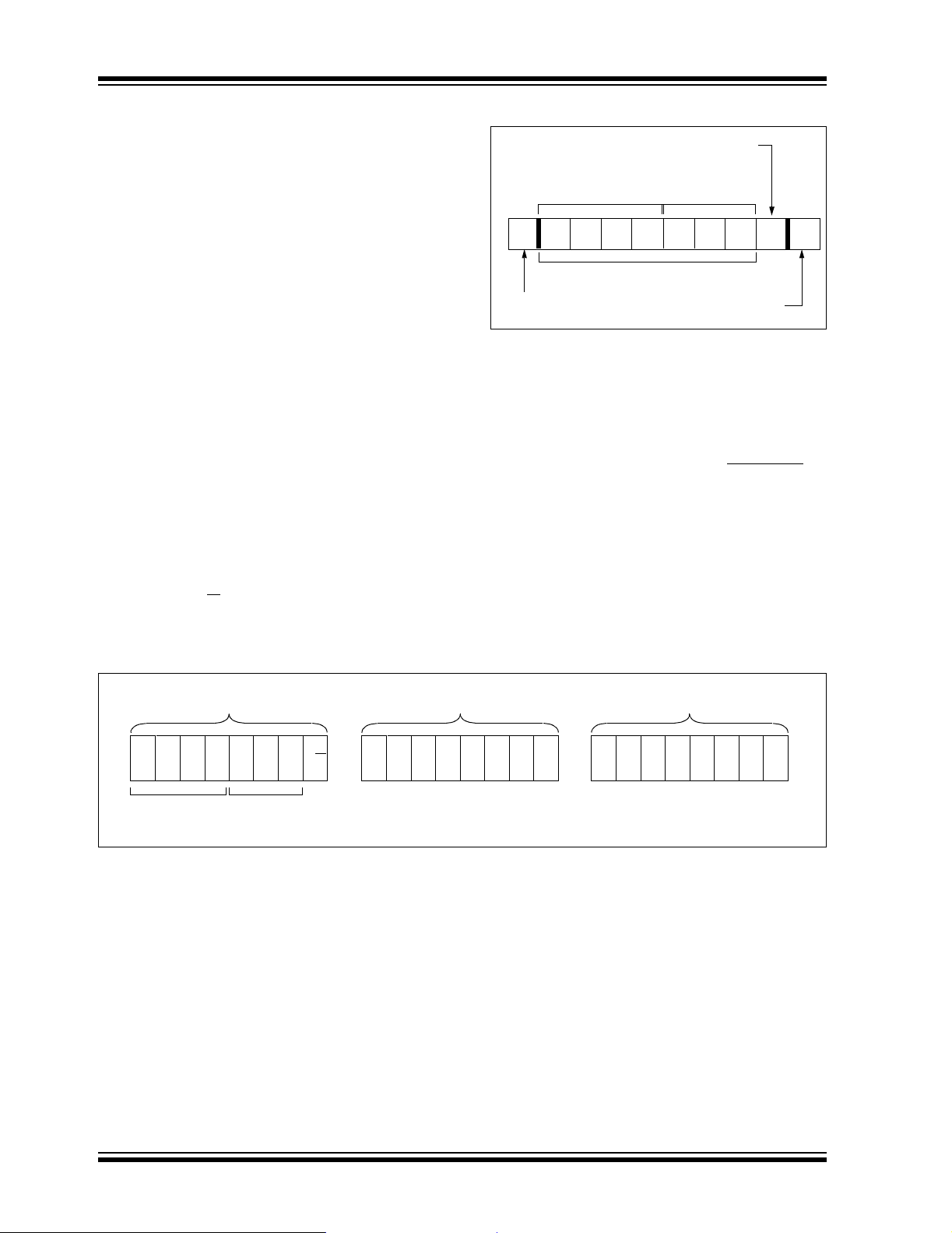
3.6 Device Addressing
A control byte is the first byte received following the
Start condition from the master device (Figure 3-2).
The control byte co nsi sts of a four-bit control cod e. For
the 24XX32A, this is set as ‘1010’ binary for read and
write operations. The ne xt th ree bits of the control byte
are the Chi p Sel ect bits ( A2, A 1, A 0). T he Chip Sele ct
bits allow the use of up to eight 24XX32A devices on
the same bus and are used to select which device is
accessed. The Chip Select bits in the control byte must
correspond to the logic lev els on the corresp onding A2,
A1, and A0 pins for the device to respond. These bits
are in effect the three Most Significant bits of the word
address.
The last bit of the control byte defines the operation to
be performed. When set to a ‘1’, a read op eration is
selected. When set to a zero, a write operation is
selected. The next two bytes received define the
address of the first data byte (Figure 3-3). Because
only A1 1 to A0 are use d, the upper four ad dress bits are
don’t care bits. The upper address bits are transferred
first, followed by the less significant bits.
Following the Start condition, the 24XX32A monitors
the SDA bus checking the device type identifier being
transmitted and, upon receiving a ‘1010’ code and
appropriate device s elect b its , the s lave d evice outputs
an Acknowledge si gnal on the SD A line. Dependi ng on
the state of the R/W
or write operation.
bit, the 24XX32A will selec t a read
FIGURE 3-2: CONTROL BYTE FORMAT
Read/Write Bit
Control Code
1 0 1 0 A2 A1 A0SACK
Slave Address
Start Bi t
Chip Select
Bits
R/W
Acknowledge Bit
3.7 Contiguous Addressing Across
Multiple Devices
The Chip Select bits A2, A1, A0 can be used to expand
the contiguous address space for up to 256K bits by
adding up to eight 24XX32A's on the same bus. In this
case, software can use A0 of the control byte
address bit A12, A1 as address bit A13, and A2 as
address bit A14. It is not possible to sequentially read
across device boundaries.
as
FIGURE 3-3: ADDRES S SEQUENCE BI T ASSIGN MENTS
CONTROL BYTE ADDRESS HIGH BYTE ADDRESS LOW BYTE
1010
CONTROL
CODE
A2A1A
CHIP
SELECT
BITS
R/W XXXX
0
A11A10A
9
A
8
A
••••••
7
X = Don’t Care B
A
0
DS21713D-page 6 2003 Microchip Technology Inc.

24AA32A/24LC32A
4.0 WRITE OPERATIONS
4.1 Byte Write
Following the Start condition from the master, the
control code (4 bits), the Chip Select (3 bits), and the
R/W bit (which is a lo gic low) ar e clo cke d on to t he b us
by the master transmitter. This indicates to the
addressed slave r eceiver that the add ress high byte
will follow once it has ge nerated an Acknowle dge bit
during the ni nth cloc k cycle. Therefor e, the n ext byte
transmitted by the master is the high-order byte of the
word address and will be written into the address
pointer of the 24XX32A. The next byte is the Least
Significant Address Byte. After receiving another
Acknowledge signal from the 24XX32A, the master
device will transmit the data word to be written into the
addressed memory loc ation. The 24XX3 2A acknowledges again and the master generates a Stop
condition. This init iates the internal write cycle and,
during this time, the 24XX32A will not generate
Acknowledge signals (Figure 4-1). If an attempt is
made to write to the array with the WP pin held high,
the device will acknowledge the command but no
write cycle will occur. No data will be writte n and the
device will immediately accept a new command. After
a byte Write command, the internal address counter
will point to the address location following the one that
was just written.
4.2 Page Write
The write control byte, word address and the first data
byte are transmitted to the 24XX32A in the same way
as in a byte write. However, instead of generating a
Stop co ndition, th e master tra nsmits up to 31 add itional
bytes whic h are tempor arily stored in the on-chip page
buffer and will be written into memory once the master
has transmitted a Stop condition. Upon receipt of each
word, the five lower-address pointer bits are internally
increment ed by ‘ 1’. If the master should transmit more
than 32 bytes prior to gene rating the S top condition, th e
address counter will roll over and the previously
received data will be overwri tten. As w ith the by te writ e
operation, once the Stop condition is received, an
internal write cycle w ill begin (Figure4-2). If an attempt
is made to write to th e array with the WP pin held hig h,
the device will ac knowledge the command but no w ri te
cycle will occur, no data will be written and the device
will immediately accept a new command.
Note: Page write operatio ns are lim ited to wri ting
bytes within a single physical page,
regardless of the number of bytes
actually being written. Physical page
boundaries start at addresses that are
integer multiples of the page buf fer size (or
‘page size’) and, end at addresses that are
integer multiples of [page size - 1]. If a
Page Write command attempts to write
across a physical page boundary, the
result is that the data wraps around to the
beginning of the current page (overwriting
data previously stored there), instead of
being written to the next p age as might be
expected. It is therefore necessary for the
application software to prevent page write
operations that would attempt to cross a
page boundary.
4.3 Write-Protection
The WP pin a llows t he user to wri te-prot ect the entire
array (0000-0FFFF) when the pin is tied to V
to V
SS or left floating, the write protection is disabled.
The WP pin is sampled at the Stop bit for every write
command (Figure 3-1) Toggling the WP pin after the
Stop bi t wil l hav e no ef fe ct on t he ex ecutio n o f the wr ite
cycle.
2003 Microchip Technology Inc. DS21713D-page 7
CC. If tied
24AA32A/24LC32A
FIGURE 4-1: BYTE WRITE
BUS ACTIVITY
MASTER
SDA LINE
BUS ACTIVITY
X = don’t care bit
FIGURE 4-2: PAGE WRITE
S
T
BUS ACTIVITY
MASTER
SDA LINE
BUS ACTIVITY
X = don’t care bit
CONTROL
A
R
T
S10 10 0
S
T
CONTROL
A
R
T
S1010 0
BYTE
A2A1A
0
A
C
K
BYTE
A
A1A
2
0
ADDRESS
HIGH BYTE
XXX
X
ADDRESS
HIGH BYTE
XXX
A
C
K
A
C
K
ADDRESS
LOW BYTE
X
A
C
K
ADDRESS
LOW BYTE DATA BYTE 0
A
C
K
S
DATA
A
C
K
DA TA BYTE 31
A
C
K
T
O
P
P
A
C
K
S
T
O
P
P
A
C
K
DS21713D-page 8 2003 Microchip Technology Inc.

24AA32A/24LC32A
5.0 ACKNOWLEDGE POLLING
Since the device will not acknowledge during a write
cycle, this can be used to determine when the cycle is
complete (this feature can be used to maximize bus
throughput). Once the Stop condition for a write
command has been issu ed from the mas ter , the device
initiates the internally-timed write cycle. ACK polling
can then be initiated immediately. This involves the
master sending a S tart c ondition fo llowed by the contro l
byte for a Write command (R/W
busy with the write cycle, then no ACK will be returned.
If no ACK is returned, the S tart bit an d control byte must
be re-sent. If the cycle is complete, the device will
return the ACK and the master can then proceed with
the next Read or Write command. See Figure 5-1 for
flow diagram of this operation.
= 0). If the device is still
FIGURE 5-1: ACKNOWLEDGE POLLING
FLOW
Send
Write Command
Send Stop
Condition to
Initiate Write Cycle
Send Start
Send Control Byte
with R/W = 0
Did Device
Acknowledge
(ACK = 0)?
YES
NO
Next
Operation
2003 Microchip Technology Inc. DS21713D-page 9

24AA32A/24LC32A
6.0 READ OPERATION
Read operations are initiated in the same way as write
operations, with the exception that the R/W
control byte is set to ‘1’. There are three basic types of
read operations: current address read, random read,
and sequential read.
6.1 Current Address Read
The 24XX32A contains an address counter that maintains the address of the last word accessed, internally
incremented by ‘1’. Therefore, if the previous read
access was to address n (n is any legal address), the
next current address read operati on would access da ta
from address n + 1.
Upon receipt of the control byte with R/W
the 24XX32A issu es an ackno wledge and t ransmits the
8- bit data word. The master will not acknowledge the
transfer but does generate a Stop condition and the
24XX32A discontinues transmission (Figure 6-1).
6.2 Random Read
Random read operati ons allow the master to access
any memory location in a random manner. To perform
this type of read operation, the word address must
first be first. This is accomplished by sending the word
address to the 24XX32A as part of a write operation
bit set to ‘0’). Once the word address is se nt, th e
(R/W
master generates a Start condition following the
acknowledge. This terminates the write operation, but
not before the internal address pointer is set. The
master issues the control byte again, but with the R/W
bit set to a ‘1’. The 24XX32A will then issue an
acknowledge and transmit the 8-bit data word. The
master will not acknowledge the transfer but does
generate a Stop condition which causes the 24XX32A
to discontinue t ransmission (Fig ure 6-2). After a random Read command, the internal address counter will
point to the address location following the one that
was just read.
bit of the
bit set to ‘1’,
6.3 Sequential Read
Sequential reads are initiated in the same way as a
random read, except that once the 24 XX32A tran sm its
the first data byte, the master issues an acknowledge
as opposed to the Stop condition used in a random
read. This acknowledge directs the 24XX32A to
transmit the next sequentially addressed 8-bit word
(Figure 6-3). Following the final byte transmitted to the
master, the master will NOT generate an acknowledge
but will generate a Stop condition. To provide sequential reads, the 24XX32A contains an internal address
pointer which is incremented by ‘1’ upon completio n of
each operation. This address pointer allows the entire
memory contents to be serially read during one
operation. The internal address pointer will automatically roll over from address FFF to address 0000 if the
master acknowledges the byte received from the array
address 0FFF.
FIGURE 6-1: CURRENT ADDRESS READ
S
BUS ACTIVITY
MASTER
SDA LINE
BUS ACTIVITY
DS21713D-page 10 2003 Microchip Technology Inc.
T
A
R
T
SP
CONTROL
BYTE
S
DA TA (n)
A
C
K
T
O
P
N
O
A
C
K

FIGURE 6-2: RANDOM READ
BUS ACTIVITY
MASTER
SDA LINE
BUS ACTIVITY
X = Don’t Care Bit
S
T
A
CONTROL
R
BYTE
T
S1010
AAA
210
0
XXX
A
C
K
ADDRESS
HIGH BYTE
FIGURE 6-3 : SEQUENTIAL READ
BUS ACTIVITY
MASTER
SDA LINE
BUS ACTIVITY
CONTROL
BYTE
DATA n DATA n + 1 DATA n + 2 DATA n + X
A
C
K
24AA32A/24LC32A
S
A
C
K
T
A
R
T
S101 0
A
C
K
CONTROL
BYTE
AAA
210
A
C
K
DATA
BYTE
1
A
C
K
ADDRESS
LOW BYTE
X
A
C
K
A
C
K
S
T
O
P
P
N
O
A
C
K
S
T
O
P
P
N
O
A
C
K
2003 Microchip Technology Inc. DS21713D-page 11

24AA32A/24LC32A
7.0 PIN DESCRIPTIONS
The descriptions of the pins are listed in Table 7-1.
TABLE 7-1: PIN FUNCTION TABLE
Name PDIP SOIC TSSOP MSOP
A0 1 1 1 1 3 Chip Address Input
A1 2 2 2 2 4 Chip Address Input
A2 3 3 3 3 5 Chip Address Input
SS 4 4 4 4 6 Ground
V
SDA 5 5 5 5 7 Serial Address/Data I/O
SCL 6 6 6 6 8 Serial Clock
WP 7 7 7 7 1 Write-Protect Input
CC 8 8 8 8 2 +1.8V to 5.5V Power Supply
V
ROTATED
TSSOP
Description
7.1 A0, A1, A2 Chip Address Inputs
The A0, A1, A2 inputs are used by the 24XX32A for
multiple device operation. The levels on these inputs
are compared with the corresponding bits in the slave
address. The chip is selected if the compare is true.
Up to eight devi ce s ma y be conn ected to th e sam e bu s
by using different Chip Select bit combinations. These
inputs must be connected to either V
CC or VSS.
7.2 Serial Data (SDA)
SDA is a bidirectional pin used to transfer addresses
and data into and out of the device. It is an open-drain
terminal, therefore, the SDA bus requires a pull-up
resistor to V
400 kHz)
For normal data transfer, SDA is allowed to change
only during SCL low. Changes during SCL high are
reserved for indicating Start and Stop conditions.
CC (typical 10 kΩ for 100 kHz, 2 kΩ for
7.3 Serial Clock (SCL)
The SCL input is used to sync hro niz e th e da ta transfer
to and from the device.
7.4 Write-Protect (WP)
The WP pin can be co nnected to either VSS, VCC or left
floating. An internal pull-down resistor on this pin will
keep the device in the unprotected state if left floating.
If tied to V
is enabled (read/write the entire memory 000-FFF).
If tied to V
operations are not affec ted .
SS, or left floating, normal memory opera tio n
CC, write operations are inhibited. Read
DS21713D-page 12 2003 Microchip Technology Inc.

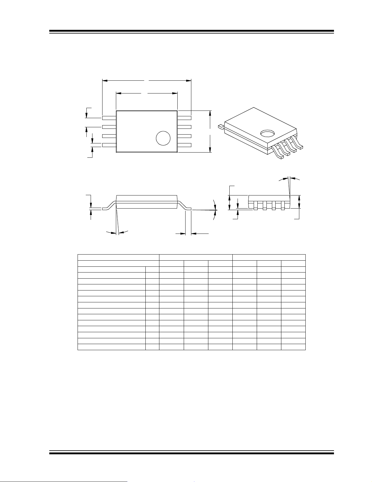
8.0 PACKAGING INFORMATION
8.1 Package Marking Information
24AA32A/24LC32A
8-Lead PDIP (300 mil)
XXXXXXXX
T/XXXNNN
YYWW
8-Lead SOIC (150 mil)
XXXXXXXX
T/XXYYWW
NNN
8-Lead SOIC (208 mil)
XXXXXXXX
T/XXXXXX
YYWWNNN
8-Lead TSSOP
XXXX
TYWW
NNN
Example:
24LC32A
I/P13F
0327
Example:
24LC32A
I/SN0327
13F
Example:
24LC32A
I/SM
032713F
Example:
4LA
I327
13F
TSSOP
Device
STD Rot Pb-free Rot
24AA32A 4AA 4AAX G4AA G4AAX
24LC32A 4LA 4LAX G4LA G4LAX
Marking Codes
8-Lead MSOP
XXXXXT
YWWNNN
Legend: XX...X Customer specific information*
T Temperature gra de (I, E)
YY Year code (last 2 digits of calendar year)
WW Week code (week of January 1 is week ‘01’)
NNN Alphanumeric traceability code
Note: In the event the full Micro chip p ar t numbe r canno t be marke d on one li ne, it w ill
be carried over to the next line t hus lim iting the number of available char acters
for customer specific information.
*Standard QTP marking consists of Microchip part number, year code, week code, and traceability code.
2003 Microchip Technology Inc. DS21713D-page 13
Example:
4L32AI
32713F
MSOP
Device
24AA32A 4A32 G4AA
24LC32A 4L32A G4LA
Note: Pb-free part number using “G” suffix
is marked on carton
Marking Codes
STD Pb-free

24AA32A/24LC32A
8-Lead Plastic Dual In-line (P) – 300 mil (PDIP)
E1
D
2
n
E
β
eB
Number of Pins
Pitch
Top to Seating Plane A .140 .155 .170 3.56 3.94 4.32
Molded Package Thickness A2 .115 .130 .145 2.92 3.30 3.68
Base to Seating Plane A1 .015 0.38
Shoulder to Shoulder Width E .300 .313 .325 7.62 7.94 8.26
Molded Package Width E1 .240 .250 .260 6.10 6.35 6.60
Overall Length D .360 .373 .385 9.14 9.46 9.78
Tip to Seating Plane L .125 .130 .135 3.18 3.30 3.43
Lead Thickness
Upper Lead Width B1 .045 .058 .070 1.14 1.46 1.78
Lower Lead Width B .014 .018 .022 0.36 0.46 0.56
Overall Row Spacing § eB .310 .370 .430 7.87 9.40 10.92
Mold Draft Angle Top
Mold Draft Angle Bottom
* Controlling Parameter
§ Significant Characteristic
Notes:
Dimensions D and E1 do not include mold flash or protrusions. Mold flash or protrusions shall not exceed
.010” (0.254mm) per side.
JEDEC Equivalent: MS-001
Drawing No. C04-018
Dimension Limits MIN NOM MAX MIN NOM MAX
1
α
A
c
Units INCHES* MILLIMETERS
n
p
c
α
β
.008 .012 .015 0.20 0.29 0.38
A1
B1
B
88
.100 2.54
51015 51015
51015 51015
A2
L
p
DS21713D-page 14 2003 Microchip Technology Inc.

8-Lead Plastic Small Outline (SN) – Narrow, 150 mil (SOIC)
E
E1
p
D
2
24AA32A/24LC32A
B
Number of Pins
Pitch
Standoff §
Foot Angle
Lead Thickness
Mold Draft Angle Top
Mold Draft Angle Bottom
* Controlling Parameter
§ Significant Characteristic
Notes:
Dimensions D and E1 do not include mold flash or protrusions. Mold flash or protrusions shall not exceed
.010” (0.254mm) per side.
JEDEC Equivalent: MS-012
Drawing No. C04-057
n
45°
c
β
n
p
A1
φ
c
α
β
1
h
A
φ
L
048048
A1
MILLIMETERSINCHES*Units
1.27.050
α
A2
MAXNOMMINMAXNOMMINDimension Limits
88
1.751.551.35.069.061.053AOverall Height
1.551.421.32.061.056.052A2Molded Package Thickness
0.250.180.10.010.007.004
6.206.025.79.244.237.228EOverall Width
3.993.913.71.157.154.146E1Molded Package Width
5.004.904.80.197.193.189DOverall Length
0.510.380.25.020.015.010hChamfer Distance
0.760.620.48.030.025.019LFoot Length
0.250.230.20.010.009.008
0.510.420.33.020.017.013BLead Width
1512015120
1512015120
2003 Microchip Technology Inc. DS21713D-page 15

24AA32A/24LC32A
8-Lead Plastic Small Outline (SM) – Medium, 208 mil (SOIC)
E
E1
p
D
2
n
B
c
β
Number of Pins
Pitch
Foot Angle
Lead Thickne ss
Mold Draft Angle Top
Mold Draft Angle Bottom
* Controlling Parameter
§ Significant Characteristic
Notes:
Dimensions D and E1 do not include mold flash or protrusions. Mold flash or protrusions shall not exceed
.010” (0.254mm) per side.
Drawing No. C04-056
n
p
φ
c
α
β
1
A
φ
L
.070 .075
.069 .074
048048
A1
1.78
1.75
MILLIMETERSINCHES*Units
1.27.050
1.97
1.88
α
A2
MAXNOMMINMAXNOMMINDimension Limits
88
2.03.080AOverall Height
1.98.078A2Molded Package Thickness
0.250.130.05.010.005.002A1Standoff §
8.267.957.62.325.313.300EOverall Width
5.385.285.11.212.208.201E1Molded Package Width
5.335.215.13.210.205.202DOverall Length
0.760.640.51.030.025.020LFoot Length
0.250.230.20.010.009.008
0.510.430.36.020.017.014BLead Width
1512015120
1512015120
DS21713D-page 16 2003 Microchip Technology Inc.
24AA32A/24LC32A
8-Lead Plastic Thin Shrink Small Outline (ST) – 4.4 mm (TSSOP)
E
E1
p
D
2
n
B
1
A
c
A1
φ
β
A1
n
p
φ
c
α
β
048048
Number of Pins
Pitch
Standoff §
Foot Angle
Lead Thickne ss
Mold Draft Angle Top
Mold Draft Angle Bottom
* Controlling Parameter
§ Significant Characteristic
Notes:
Dimensions D and E1 do not include mold flash or protrusions. Mold flash or protrusions shall not exceed
.005” (0.127mm) per side.
JEDEC Equivalent: MO-153
Drawing No. C04-086
L
MILLIMETERS*INCHESUnits
0.65.026
α
A2
MAXNOMMINMAXNOMMINDimension Limits
88
1.10.043AOverall Height
0.950.900.85.037.035.033A2Molded Package Thickness
0.150.100.05.006.004.002
6.506.386.25.256.251.246EOverall Width
4.504.404.30.177.173.169E1Molded Package Width
3.103.002.90.122.118.1 14DMolded Package Length
0.700.600.50.028.024.020LFoot Length
0.200.150.09.008.006.004
0.300.250.19.012.010.007BLead Width
10501050
10501050
2003 Microchip Technology Inc. DS21713D-page 17

24AA32A/24LC32A
8-Lead Plastic Micro Small Outline Package (MS) (MSOP)
E
E1
p
D
2
B
n 1
α
A
c
(F)
β
Units
Dimension Limits
Number of Pins
Pitch
Overall Height
Molded Package Thickness
Standoff
Overall Width
Molded Package Width
Overall Length
Foot Length
Foot Angle
Lead Thickness
Lead Width
Mold Draft Angle Top
Mold Draft Angle Bottom
*Controlling Parameter
Notes:
Dimensions D and E1 do not include mold flash or protrusions. Mold flash or protrusions shall not
exceed .010" (0.254mm) per side.
JEDEC Equivalent: MO-187
Drawing No. C04-111
A2
A1
E1
MIN
n
p
A
E
D
L
φ
c
B
α
β
.026 BSC
.030
.000
.193 TYP.
.118 BSC
.118 BSC
.016 .024
.037 REFFFootprint (Reference)
0° - 8°
.003
.009
5°
5° -
L
INCHES
NOM
.033
.006
.012
φ
A1
MAX NOM
8
--
-
-
.043
.037
.006
.031
.009
.016
15°
15°
MIN
0.75
0.00
0.40
0.08
0.22
MILLIMETERS*
MAX
8
0.65 BSC
--
0.85
-
4.90 BSC
3.00 BSC
3.00 BSC
0.60
0.95 REF
0°
-
-
-
A2
1.10
0.95
0.15
0.80
8°
0.23
0.40
15°5° 15°5° -
DS21713D-page 18 2003 Microchip Technology Inc.

APPENDIX A: REVISION HISTORY
Revision D
Corrections to Section 1.0, Electrical Characteristics.
24AA32A/24LC32A
2003 Microchip Technology Inc. DS21713D-page 19

24AA32A/24LC32A
NOTES:
DS21713D-page 20 2003 Microchip Technology Inc.

24AA32A/24LC32A
ON-LINE SUPPORT
Microchip provides on-line support on the Microchip
World Wide Web site.
The web site is used b y Mic rochip as a me ans to m ake
files and information easily available to customers. To
view the site, the use r must have access to the Intern et
and a web browser, such as Netscape
Internet Explorer. Files are also available for FTP
download from our FTP site.
Connecting to the Microchip Internet
Web Site
The Microchip web site is available at the following
URL:
www.microchip.com
The file transfer site is available by using an FTP
service to connect to:
ftp://ftp.microchip.com
The web site and file transfer site provide a variety of
services. Users may download files for the latest
Development Tools, Data Sheets, Application Notes,
User's Guides, Articles and Sample Programs. A variety of Micr ochip specific bu siness informatio n is also
available, including listings of Microchip sales offices,
distributors and factory representatives. Other data
available for consideration is:
• Latest Microchip Press Releases
• Technical Support Section with Frequently Asked
Questions
• Design Tips
• Device Errata
• Job Postings
• Microchip Consultant Program Member Listing
• Links to other useful web sites related to
Microchip Products
• Conferences for p roducts, D evelopment Systems,
technical information and more
• Listing of seminars and events
®
or Microsoft
SYSTEMS INFORMATION AND UPGRADE HOT LINE
The Systems Information and Upgrade Line provides
system users a listing of the latest versions of all of
Microchip's development systems software products.
®
Plus, this line provides information on how customers
can receive the most c urrent upgrade kit s. The Hot Line
Numbers are:
1-800-755-2345 for U.S. and most of Canada, and
1-480-792-7302 for the rest of the world.
042003
2003 Microchip Technology Inc. DS21713D-page 21

24AA32A/24LC32A
READER RESPONSE
It is our intentio n to pro vi de you with the best documentation possible to ens ure suc c es sfu l u se of y ou r M ic roc hip product. If you wish to provid e your c omment s on org anizatio n, clarity, subject matter , and ways in wh ich our d ocument ation
can better serve you, please FAX your comments to the Technical Publications Manager at (480) 792-4150.
Please list the following information, and use this outline to provide us with your comments about this document.
To:
RE: Reader Response
From:
Application (optional):
Would you like a reply? Y N
Device: Literature Number:
Questions:
1. What are the best features of this document?
2. How does this document meet your hardware and software development needs?
3. Do you find the organization of this document easy to follow? If not, why?
Technical Publications Manager
Name
Company
Address
City / State / ZIP / Country
Telephone: (_______) _________ - _________
Total Pages Sent ________
FAX: (______) _________ - _________
DS21713D24AA32A/24LC32A
4. What additions to the document do you think would enhance the structure and subject?
5. What deletions from the document could be made without affecting the overall usefulness?
6. Is there any incorrect or misleading information (what and where)?
7. How would you improve this document?
DS21713D-page 22 2003 Microchip Technology Inc.

24AA32A/24LC32A
,
PRODUCT IDENTIFICATION SYSTEM
To order or obtain information, e.g., on pricing or delivery, refer to the factory or the listed sales office.
PART NO.
Device
X /XX
PackageTemperature
X
Lead Finish
Range
Device: 24AA32A: 1.8V, 32 Kbit I2C Serial EEPROM
24AA32AT: 1.8V, 32 Kbit I
24AA32AX 1.8V, 32 Kbit I
24AA32AXT 1.8V, 32 Kbit I
24LC32A: 2.5V, 32 Kbit I
24LC32AT: 2.5V, 32 Kbit I
24LC32AX 2.5V, 32 Kbit I
24LC32AXT 2.5V, 32 Kbit I
Temperature
Range:
Package: P = Plastic DIP (300 mil body), 8-lead
Lead Finish Blank = Standard 63% / 37% SnPb
I = -40°C to +85°C
E = -40°C to +125°C
SN = Plastic SOIC (150 mil body), 8-lead
SM = Plastic SOIC (208 mil body), 8-lead
ST = Plastic TS SO P (4. 4 mm), 8-lead
MS = Plastic Micro Small Outline (MSOP), 8-lead
G = Pb-free (Matte Tin - Pure Sn)
(Tape and Reel)
alternate pinout (ST only)
alternate pinout (ST only)
(Tape and Reel)
alternate pinout (ST only)
alternate pinout (ST only)
2
C Serial EEPROM
2
C Serial EEPROM in
2
C Serial EEPROM in
2
C Serial EEPROM
2
C Serial EEPROM
2
C Serial EEPROM in
2
C Serial EEPROM in
Examples:
a) 24AA32A-I/P: Industrial Temperature,1.8V,
PDIP package
b) 24AA32A-I/SN: Industrial Temperature,1.8V,
SOIC package
c) 24AA32A-I/SM: Industrial Temperature.,1.8V,
SOIC (208 mil) package
d) 24AA32AX -I/ST: Industrial Temp.,1.8V,
Rotated TSSOP package
e) 24AA32A-I/ST: Industrial Temperature.,1.8V,
TSSOP packa ge
f) 24AA32A-I/PG: Industrial Temperature.,1.8V,
PDIP package. Pb-free
g) 24LC32A-I/P: Industrial Temperature, 2.5V,
PDIP package
h) 24LC32A-E/SN: Automotive Temperature
2.5V SOIC package
i) 24LC32A -E/ SM : Automotive Temperature,
2.5V SOIC (208 mil) package
j) 24LC32AX-E/ST: Automotive Temperature,
2.5V, Rotated TSSOP package
k) 24LC32AT-I/ST: Industrial Temperature, 2.5V,
TSSOP package, Tape and Reel
l) 24LC32AT-I/SNG: Industrial Temperature,
2.5V , SOIC package, Tape and Reel, Pb-free
Sales and Support
Data Sheets
Products supported by a preliminary Data Sheet may have an errata sheet describing minor operational differences and
recommended workarounds. To determine if an errata sheet exists for a particular device, please contact one of the following:
1. Your local Microchip sales office
2. The Microchip Corporate Literature Center U.S. FAX: (480) 792-7277
3. The Microchip Worldwide Site (www.microchip.com)
Please specify which device, revision of silicon and Data Sheet (include Literature #) you are using.
New Customer Notification System
Register on our web site (www.microchip.com/cn) to receive the most current information on our products.
2003 Microchip Technology Inc. DS21713D-page 23

24AA32A/24LC32A
NOTES:
DS21713D-page 24 2003 Microchip Technology Inc.

Note the following details of the code protection feature on Microchip devices:
• Microchip products meet the specification contained in their particular Microchip Data Sheet.
• Microchip believes that its family of products is one of the most secure families of its kind on the market today, when used in the
intended manner and under normal conditions.
• There are dishonest and possibly illegal methods used to breach the code protection feature. All of these methods, to our
knowledge, require using the Microchip products in a manner outside the operating specifications contained in Microchip's Data
Sheets. Most likely, the person doing so is engaged in theft of intellectual property.
• Microchip is willing to work with the customer who is concerned about the integrity of their code.
• Neither Microchip nor any other semiconductor manufacturer can guarantee the security of their code. Code protection does not
mean that we are guaranteeing the product as “unbreakable.”
Code protection is constantly evolving. We at Microchip are committed to continuously improving the co de protection fea tures of our
products. Attempts to break microchip’s code protection feature may be a violation of the Digital Millennium Copyright Act. If such acts
allow unauthorized access to your software or other copyrighted work, you may have a right to sue for relief under that Act.
Information contained in this publication regarding device
applications and the like is intended through suggestion only
and may be superseded by updates. It is your responsibility to
ensure that your application meets with your specifications.
No representation or warranty is given and no liability is
assumed by Microchip Technology Incorporated with respect
to the accuracy or use of such information, or infringement of
patents or other intellectual property rights arising from such
use or otherwise. Use of Microchip’s products as critical components in life support systems is not authorized except with
express written approval by Microchip. No licenses are conveyed, implicitly or otherwise, under any intellectual property
rights.
Trademarks
The Microchip name and logo, the Microchip logo, Accuron,
dsPIC, K
EELOQ, MPLAB, PIC, PICmic ro, PI C START,
PRO MATE and PowerSmart are registered trademarks of
Microchip Technology Incorporated in the U.S.A. and other
countries.
AmpLab, FilterLab, microID, MXDEV, MXLAB, PI CMASTER,
SEEVAL and The Embedded Control Solutions Company are
registered trademarks of Microchip Technology Incorporated
in the U.S.A.
Application Maestro, dsPICDEM, dsPICDEM.net, ECAN,
ECONOMONITOR, FanSense, FlexROM, fuzzyLAB,
In-Circuit Serial Programming, ICSP, ICEPIC, microPort,
Migratable Memory, MPASM, MPLIB, MPLINK, MPSIM,
PICkit, PICDEM, PICDEM.net, PowerCal, PowerInfo,
PowerMate, PowerTool, rfLAB, rfPIC, Select Mode,
SmartSensor, SmartShunt, SmartT el and Total Endurance are
trademarks of Microchip Technology Incorporated in the
U.S.A. and other countries.
Serialized Quick Turn Programming (SQTP) is a service mark
of Microchip Technology Incorporated in the U.S.A.
All other trademarks mentioned herein are property of their
respective companies.
© 2003, Microchip Technology Incorporated, Printed in the
U.S.A., All Rights Reserved.
Printed on recycled paper.
Microchip received QS-9000 quality system
certification for its worldwide headquarters,
design and wafer fabrication facilities in
Chandler and Tempe, Arizona in July 1999
and Mountain View, California in March 2002.
The Company’s quality system processes and
procedures are QS-9000 compliant for its
PICmicro
devices, Serial EEPROMs, microperipherals,
non-volatile memory and analog products. In
addition, Microchip’s quality system for the
design and manufacture of development
systems is ISO 9001 certified.
®
8-bit MCUs, KEELOQ
®
code hopping
2003 Microchip Technology Inc. DS21713D-page 25

WORLDWIDE SALES AND SERVICE
AMERICAS
Corporate Office
2355 West Chandler Blvd.
Chandler, AZ 85224-6199
Tel: 480-792-72 00
Fax: 480-792-7277
Technical Support: 480-792-7627
Web Address: http://www.microchip.com
Atlanta
3780 Mansell Road, Suite 130
Alpharetta, GA 30022
Tel: 770-640- 003 4
Fax: 770-640-0307
Boston
2 Lan Drive, Suite 120
Westford, MA 01886
Tel: 978-692- 384 8
Fax: 978-692-3821
Chicago
333 Pierce Road, Suite 180
Itasca, IL 60143
Tel: 630-285- 007 1
Fax: 630-285-0075
Dallas
4570 Westgrove Drive, Suite 160
Addison, TX 75001
Tel: 972-818- 742 3
Fax: 972-818-2924
Detroit
Tri-Atria Office Building
32255 Northwestern Highway, Suite 190
Farmington Hills, MI 48334
Tel: 248-538- 225 0
Fax: 248-538-2260
Kokomo
2767 S. Albright Road
Kokomo, IN 46902
Tel: 765-864- 836 0
Fax: 765-864-8387
Los Angeles
18201 Von Karman, Suite 1090
Irvine, CA 92612
Tel: 949-263- 188 8
Fax: 949-263-1338
Phoenix
2355 West Chandler Blvd.
Chandler, AZ 85224-6199
Tel: 480-792-79 66
Fax: 480-792-4338
San Jose
2107 North First Street, Suite 590
San Jose, CA 95131
Tel: 408-436- 795 0
Fax: 408-436-7955
Toronto
6285 Northam Drive, Suite 108
Mississauga, Ontario L4V 1X5, Cana da
Tel: 905-673- 069 9
Fax: 905-673-6509
ASIA/PACIFIC
Australia
Suite 22, 41 Rawson Street
Epping 2121, NSW
Australia
Tel: 61-2-986 8-6 73 3
Fax: 61-2-9868-6755
China - Beijing
Unit 915
Bei Hai Wan Tai Bldg.
No. 6 Chaoyangmen Beidajie
Beijing, 100027, No. China
Tel: 86-10-85 282 10 0
Fax: 86-10-85282104
China - Chengdu
Rm. 2401-2402, 24th Floor,
Ming Xing Financial Tower
No. 88 TIDU Street
Chengdu 610016, China
Tel: 86-28-86 766 20 0
Fax: 86-28-86766599
China - Fuzhou
Unit 28F, World Trade Plaza
No. 71 Wusi Road
Fuzhou 350001, China
Tel: 86-591-7 503 50 6
Fax: 86-591-7503521
China - Hong Kong SAR
Unit 901-6, Tower 2, Metroplaza
223 Hing Fong Road
Kwai Fong, N.T., Hong Kong
Tel: 852-2401 -12 00
Fax: 852-2401-3431
China - Shanghai
Room 701, Bldg. B
Far East International Plaza
No. 317 Xian Xia Road
Shanghai, 200051
Tel: 86-21-62 75- 57 00
Fax: 86-21-6275-5060
China - Shenzhen
Rm. 1812, 18/F, Building A, United Plaza
No. 5022 Binhe Road, Futian District
Shenzhen 518033, China
Tel: 86-755-8 290 13 80
Fax: 86-755-8295-1393
China - Shunde
Room 401, Hongjian Building
No. 2 Fengxiangnan Road, Ronggui Town
Shunde City, Guangdong 528303, China
Tel: 86-765-8395507 Fax: 86-765-8395571
China - Qingdao
Rm. B505A, Fullhope Plaza,
No. 12 Hong Kong Central Rd.
Qingdao 266071, China
Tel: 86-532-5027355 Fax: 86-532-5027205
India
Divyasree Chambers
1 Floor, Wing A (A3/A4)
No. 11, O’Shaugnessey Road
Bangalore, 560 025, India
Tel: 91-80-2290061 Fax: 91-80-2290062
Japan
Benex S-1 6F
3-18-20, Shinyokohama
Kohoku-Ku, Yokohama-shi
Kanagawa, 222-0033, Japan
Tel: 81-45-47 1- 616 6 Fax: 81-4 5-4 71 -6122
Korea
168-1, Youngbo Bldg. 3 Floor
Samsung-Dong, Kangnam-Ku
Seoul, Korea 135-882
Tel: 82-2-554-7200 Fax: 82-2-558-5932 or
82-2-558-5934
Singapore
200 Middle Road
#07-02 Prime Centre
Singapore, 188980
Tel: 65-6334-8870 Fax: 65-6334-8850
Taiwan
Kaohsiung Branch
30F - 1 No. 8
Min Chuan 2nd Road
Kaohsiung 806, Taiwan
Tel: 886-7-536-4818
Fax: 886-7-536-4803
Taiwan
Taiwan Branch
11F-3, No. 207
Tung Hua North Road
Taipei, 105, Taiwan
Tel: 886-2-2717-7175 Fax: 886-2-2545-0139
EUROPE
Austria
Durisolstrasse 2
A-4600 Wels
Austria
Tel: 43-7242-2244-399
Fax: 43-7242-2244-393
Denmark
Regus Business Centre
Lautrup hoj 1-3
Ballerup DK-2750 Denmark
Tel: 45-4420-9895 Fax: 45-4420-9910
France
Parc d’Activite du Moulin de Massy
43 Rue du Saule Trapu
Batiment A - ler Etage
91300 Massy, France
Tel: 33-1-69-53-63-20
Fax: 33-1-69-30-90-79
Germany
Steinheilstrasse 10
D-85737 Ismaning, Germany
Tel: 49-89-627-144-0
Fax: 49-89-627-144-44
Italy
Via Quasimodo, 12
20025 Legnano (MI)
Milan, Italy
Tel: 39-0331-742611
Fax: 39-0331-466781
Netherlands
P. A. De Biesbosch 14
NL-5152 SC Drunen, Netherlands
Tel: 31-416-690399
Fax: 31-416-690340
United Kingdom
505 Eskdale Road
Winnersh Triangle
Wokingham
Berkshir e, England RG41 5T U
Tel: 44-118-921-5869
Fax: 44-118-921-5820
07/28/03
DS21713D-page 26 2003 Microchip Technology Inc.
 Loading...