

Page 1
24LC21A
1K 2.5V Dual Mode I2C™ Serial EEPROM
Features
• Single supply with operation down to 2.5V
• Completely implements DDC1™/DDC2™
interface for monitor identification, including
recovery to DDC1
• Pin and function compatible with 24LC21
• Low-power CMOS technology
- 1 mA typical active current
-10 µA standby current typical at 5.5V
• 2-wire serial interface bus, I
2
C™ compatible
• 100 kHz (2.5V) and 400 kHz (5V) compatibility
• Self-timed write cycle (including auto-erase)
• Page write buffer for up to eight bytes
• 1,000,000 erase/write cycles ensured
• Data retention > 200 years
• ESD Protection > 4000V
• 8-pin PDIP and SOIC package
• Available for extended temperature ranges
- Commercial (C): 0°C to +70°C
- Industrial (I): -40°Cto +85°C
Description
The Microchip Technology Inc. 24LC21A is a 128x 8-bit
dual-mode Electrically Erasable PROM. This device is
designed for use in applications requiring storage and
serial transmission of configuration and control information. Two modes of operation have been implemented:
Transmit-only mode and Bidirectional mode. Upon
power-up, the device will be in the Transmit-only mode,
sending a serial bit stream of the memory array from 00h
to 7Fh, clocked by the VCLK pin. A valid high-to-low
transition on the SCL pin will cause the device to enter
the transition mode, and look for a valid control byte on
2
C bus. If it detects a valid control byte from the
the I
master, it will switch into Bidirectional mode, with byte
selectable read/write capability of the memory array
using SCL. If no control byte is received, the device will
revert to the Transmit-only mode after it receives 128
consecutive VCLK pulses while the SCL pin is idle. The
24LC21A is available in a standard 8-pin PDIP and
SOIC package in both commercial and industrial
temperature ranges.
DDC is a trademark of the Video Electronics Standards
Association.
2
C is a trademark of Philips Corporation.
I
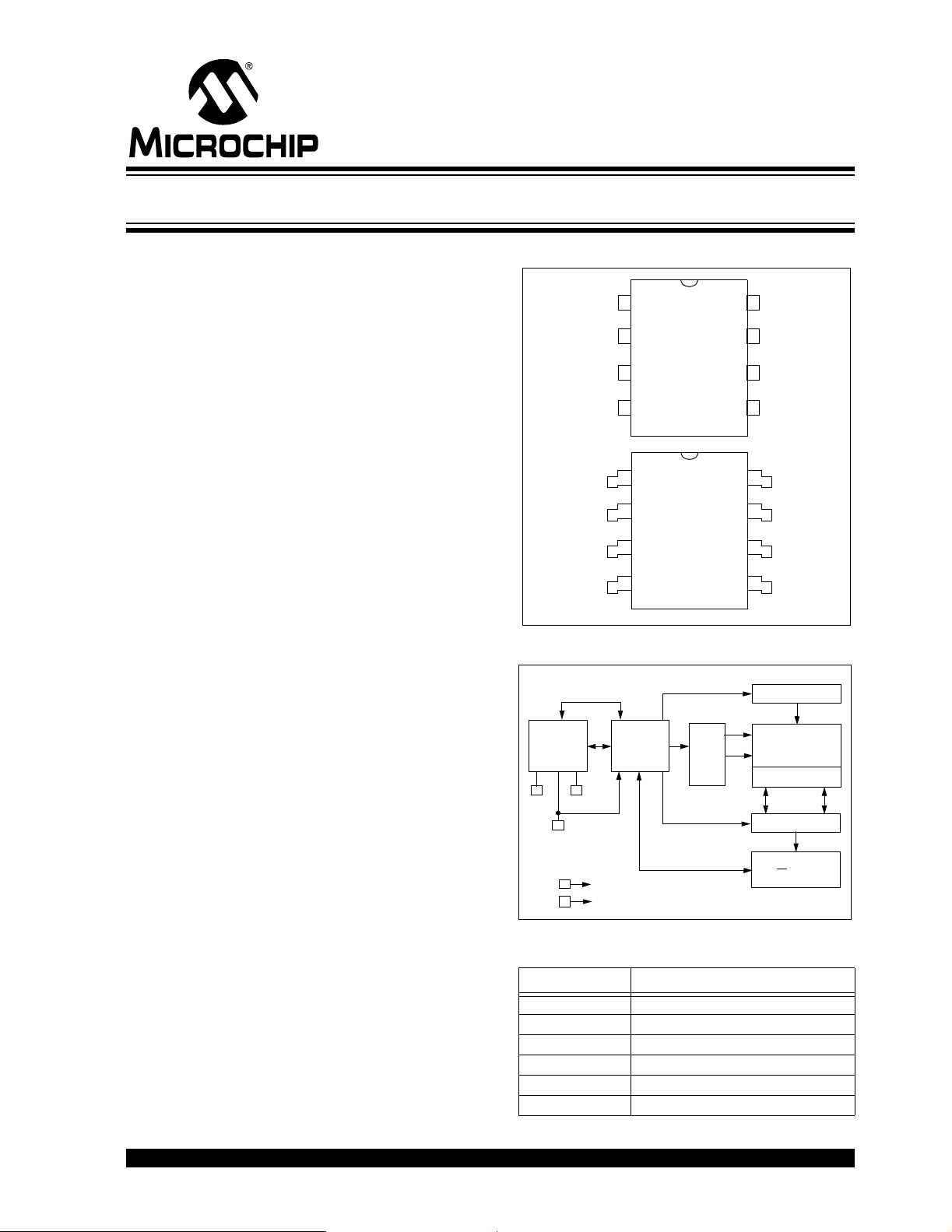
Package Types
PDIP
NC
1
8
24LC21A
NC
V
NC
SS
2
3
4
7
6
5
SOIC
NC
1
8
24LC21A
NC
NC
Vss
2
3
4
7
6
5
Block Diagram
SDA
V
VSS
I/O
Control
Logic
SCL
VCLK
CC
Memory
Control
Logic
XDEC
Pin Function Table
Name Function
SS Ground
V
SDA Serial Address/Data I/O
SCL Serial Clock (Bidirectional mode)
VCLK Serial Clock (Transmit-only mode)
V
CC +2.5V to 5.5V Power Supply
NC No Connection
Vcc
VCLK
SCL
SDA
Vcc
VCLK
SCL
SDA
HV Generator
EEPROM
Array
Page Latches
YDEC
Sense AMP
Control
R/W
2003 Microchip Technology Inc. DS21160F-page 1
Page 2
24LC21A
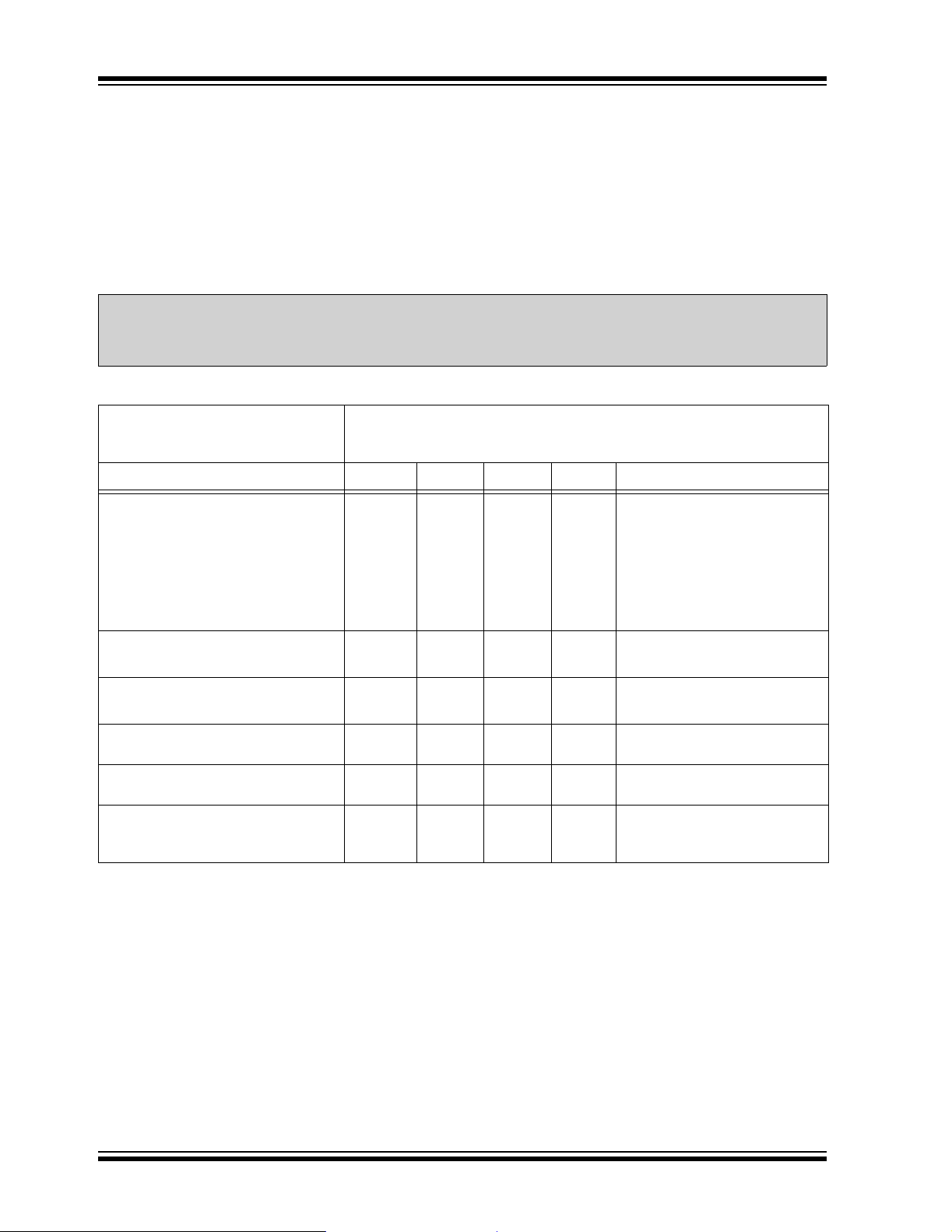
1.0 ELECTRICAL CHARACTERISTICS
Absolute Maximum Ratings
(†)
VCC.............................................................................................................................................................................7.0V
All inputs and outputs w.r.t. V
SS.........................................................................................................................................-0.6V to VCC +1.0V
Storage temperature ...............................................................................................................................-65°C to +150°C
Ambient temperature with power applied................................................................................................-65°C to +125°C
ESD protection on all pins ......................................................................................................................................................≥ 4 kV
† NOTICE: Stresses above those listed under “Absolute Maximum Ratings” may cause permanent damage to
the device. This is a stress rating only and functional operation of the device at those or any other conditions
above those indica ted in the opera tional li stings of this sp ecification is not i mplied. Ex posure to maximum rating
conditions for extended periods may affect device reliability.
TABLE 1-1: DC CHARACTERISTICS
VCC = +2.5V to 5.5V
DC CHARACTERISTICS
Commercial (C): T
Industrial (I): T
Parameter Symbol Min Max Units Conditions
SCL and SDA pins:
High-level input voltage
Low-level input voltage
VIH
VIL
Input levels on VCLK pin:
High-level input voltage
Low-level input voltage
Hysteresis of Schmitt Trigger inputs V
Low-level output voltage V
Low-level output voltage V
Input leakage current I
IH
V
VIL
HYS .05 VCC —V(Note)
OL1 —0.4VIOL = 3 mA, VCC = 2.5V (Note)
OL2 —0.6VIOL = 6 mA, VCC = 2.5V
LI —±1µAVIN = 0.1V to VCC
Output leakage current ILO —±1µAVOUT = 0.1V to VCC
Pin capacitance (all inputs/outputs) CIN, COUT —10pFVCC = 5.0V (Note)
Operating current I
Standby current I
CC Write
CC Read
I
CCS —
Note: This parameter is periodically sampled and not 100% tested.
A = 0°C to +70°C
A =-40°C to +85°C
0.7 VCC
—
2.0
—
—
—
—
—
0.3 VCC
—
CC
0.2 V
3
1
30
100
V
V
V
VCC ≥ 2.7V (Note)
V
mAmAV
CC < 2.7V (Note)
V
T
A = 25°C, FCLK = 1 MHz
CC = 5.5V
CC = 5.5V, SCL = 400 kHz
V
µAµAVCC = 3.0V, SDA = SCL = VCC
VCC = 5.5V, SDA = SCL = VCC
VCLK = VSS
DS21160F-page 2 2003 Microchip Technology Inc.
Page 3
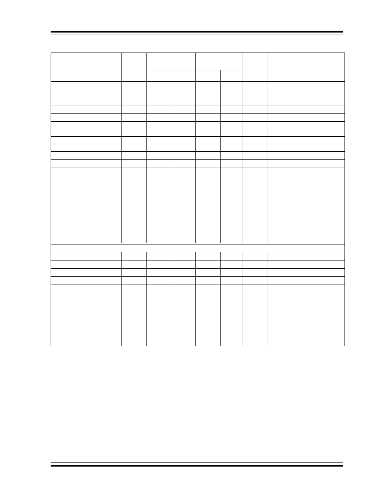
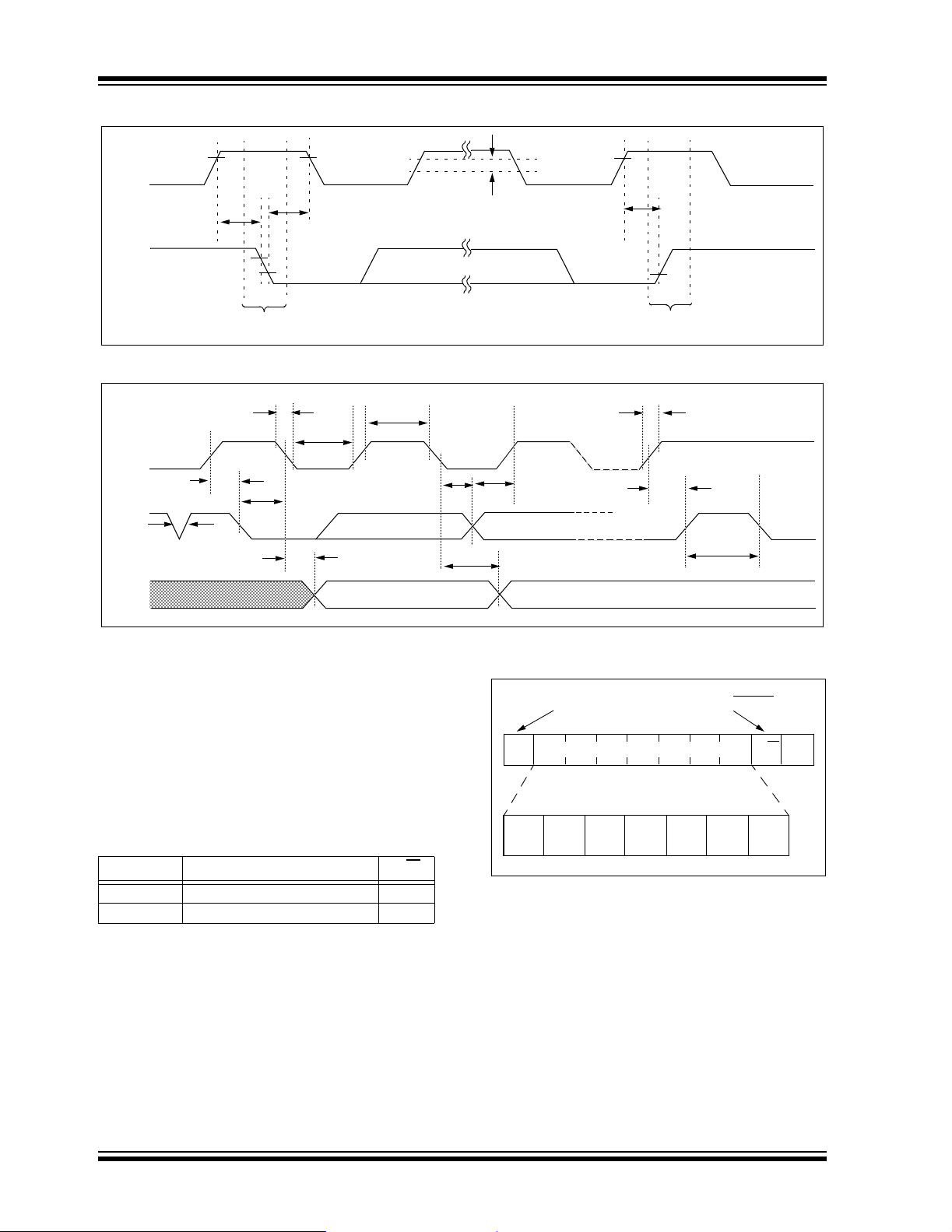
TABLE 1-2: AC CHARACTERISTICS
24LC21A
Parameter Symbol
Vcc= 2.5-5.5V
Standard Mode
Vcc= 4.5 - 5.5V
Fast Mode
Units Remarks
Min Max Min Max
Clock frequency F
CLK —100—400kHz
Clock high time THIGH 4000 — 600 — ns
Clock low time TLOW 4700 — 1300 — ns
SDA and SCL rise time T
R — 1000 — 300 ns (Note 1)
SDA and SCL fall time TF — 300 — 300 ns (Note 1)
Start condition hold time THD:STA 4000 — 600 — ns After this period the first cloc k
pulse is generated
Start condition setup time T
SU:STA 4700 — 600 — ns Only relevant for repeated
Start condition
Data input hold time T
Data input setup time T
HD:DAT 0—0—ns(Note 2)
SU:DAT 250 — 100 — ns
Stop condition setup time TSU:STO 4000 — 600 — ns
Output valid from clock TAA — 3500 — 900 ns (Note 2)
Bus free time T
BUF 4700 — 1300 — ns Time the bus must be free
before a new transmission
can start
Output fall time from VIH
minimum to V
IL maximum
Input filter spike suppres-
T
OF — 250 20 + 0.1
C
SP —50—50ns(Note 3)
T
250 ns (Note 1), CB ≤ 100 pF
B
sion (SDA and SCL pins)
Write cycle time T
WR — 10 — 10 ms Byte or Page mode
Transmit-Only Mode Parameters
Output valid from VCLK T
VAA — 2000 — 1000 ns
VCLK high time TVHIGH 4000 — 600 — ns
VCLK low time T
VLOW 4700 — 1300 — ns
VCLK setup time TVHST 0—0—ns
VCLK hold time TSPVL 4000 — 600 — ns
Mode transition time T
Transmi t-onl y power-up
VHZ — 1000 — 500 ns
TVPU 0—0—ns
time
Input filter spike suppres-
SPV — 100 — 100 ns
T
sion (VCLK pin)
Endurance — 1M — 1M — cycles 25°C, Vcc = 5.0V, Block
mode (Note 4)
Note 1: Not 100% tested. C
B = Total capacitance of one bus line in pF.
2: As a transmitter, the device must provide an internal minimum delay time to bridge the undefined region
(minimum 300 ns) of the falling edge of SCL to avoid unintended generation of Start or Stop conditions.
3: The combined T
spike suppression. This eliminates the need for a T
SP and VHYS specifications are due to Schmitt Trigger inputs which provide noise and
I specification for standard operation.
4: T his parameter is not tested but ensured by characterization. For endurance estimates in a specific
application, please consult the Total Endurance™ Model which can be obtained from our web site.
2003 Microchip Technology Inc. DS21160F-page 3
Page 4
24LC21A
2.0 FUNCTIONAL DESCRIPTION
The 24LC21A is designed to comply to the DDC
Standard proposed by VESA (Figure 3-3) with the
exception that it is not Access.bus cap ab le. I t operates
in two modes, the Transmit-only mode and the
Bidirectional mode. T here is a sep ara te 2- wire prot ocol
to support each mode, each having a separate clock
input but sharing a common data line (SDA). The
device enters the Transmit-only mode upon power-up.
In this mode, the dev ice t ransm its dat a bit s o n the SD A
pin in response to a clock signal on the VCLK pin. The
device will remain in this mode until a valid high-to-low
transition is placed on the SCL input. When a valid
transition on SCL is recognized, the device will switch
into the Bidirectional mode and look for its control byte
to be sent by the master. If it detects its control byte, it
will stay in the Bidirectional mode. Otherwise, it will
revert to the Transmit-only mode after it sees 128
VCLK pulses.
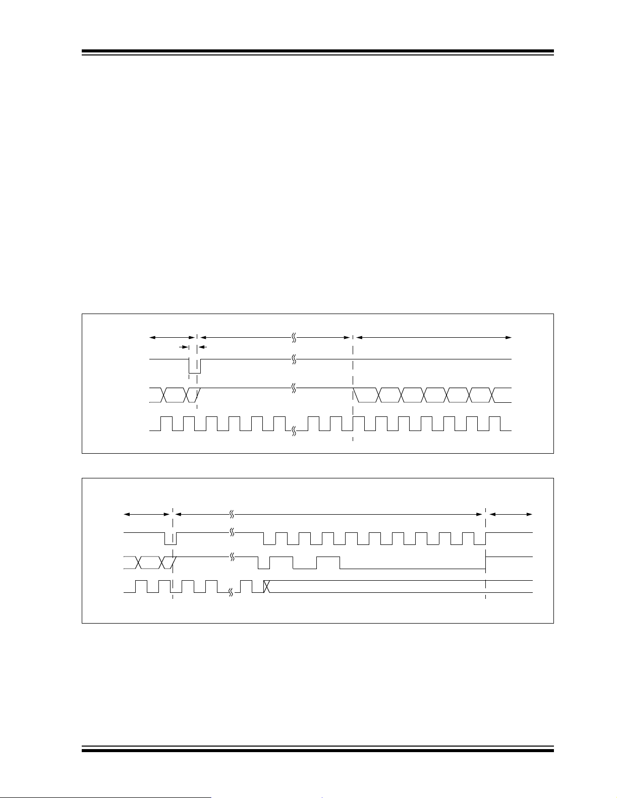
2.1 Transmit-Only Mode
The device will power-up in the Transmit-only mode at
address 00H. This mode supports a unidirectional
2-wire protocol for continuous transmission of the
contents of th e memory a rray. This d evice requi res that
it be initialized prior to valid data being sent in the
Transmit-only mode (Section 2.2 “Initialization Pro-
cedure”). In this mod e, data is trans mitted on the SDA
pin in 8-bit bytes, with each byte followed by a ninth,
null bit (Figure 2-1). The clock source for the Transmitonly mode is provided on the VCLK pin, and a data bit
is output on the rising edge on this pin. Th e eight bit s in
each byte are transmitted Most Significant bit first.
Each byte within the memory array will be output in
sequence. After address 7Fh in the memory array is
transmitted, the internal address pointers will wrap
around to the first memory loca tion (00h) and conti nue.
The Bidirectional mode Clock (SCL) pin must be held
high for the device to remain in the Transmit-only
mode.
2.2 Initialization Procedure
After VCC has stabilized, the device will be in the
Transmit -only mode. Nine clock cy cles on the VCL K pin
must be given to the device for it to perform internal
sychronization. During this period, the SDA pin will be
in a high-impedance state. On the rising edge of the
tenth clock cycle, the device will output the first valid
data bit which will be the Most Significant bit in address
00h. (Figure 2-2).
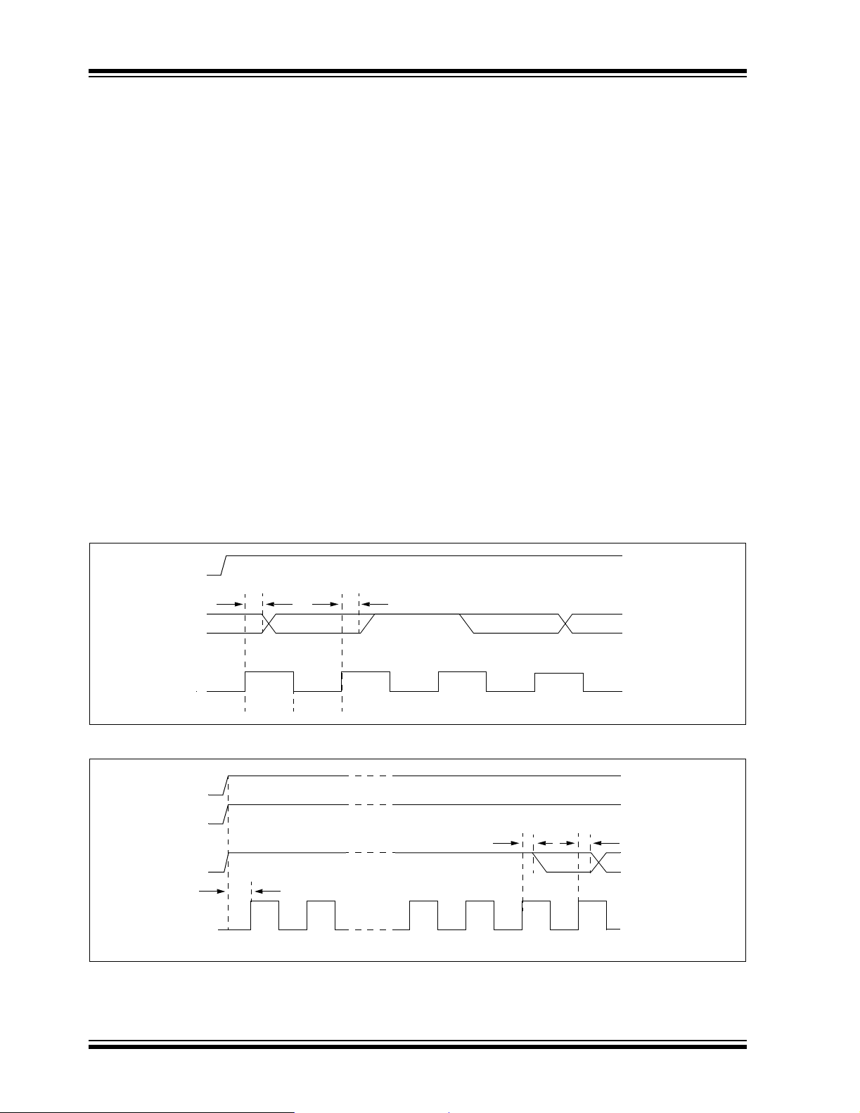
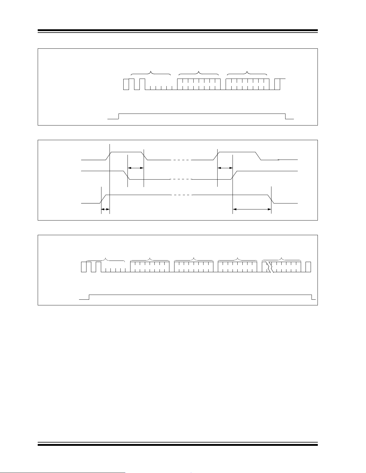
FIGURE 2-1: TRANSMIT-ONLY MODE
SCL
Tvaa Tvaa
SDA
Bit 1 (LSB)
VCLK
TvlowTvhigh
FIGURE 2-2: DEVICE INITIALIZATION
Vcc
SCL
SDA
Tvpu
VCLK
12 891011
Null Bit
Bit 1 (MSB) Bit 7
Tvaa Tvaa
Bit 8 Bit 7High-impedance for 9 clock cycles
DS21160F-page 4 2003 Microchip Technology Inc.
Page 5
24LC21A
3.0 BIDIRECTIONAL MODE
Before the 24LC21A can be switched into the
Bidirectional mode (Figure3-1), it must enter the
Transition mode, which is done by applying a valid
high-to-low transition on the Bidirectional mode Clock
(SCL). As soon it enters the Transition mode, it looks
for a control byte 1010 000X on the I
starts to count pulses on VCLK. Any high-to-low transition on the SCL line will reset the count. If it sees a
pulse count of 128 on VCLK while the SCL line is idle,
it will revert back to the Transmit-only mode, and
transmit its contents starting with the Most Significant
bit in address 00h. However, if it detects the control
byte on the I
in the Bidirectional mode. Once the device has made
the transition to the Bidire ctiona l mode , the onl y way to
switch the device back to the Transmit-only mode is to
remove power from the device. The mode transition
process is shown in detail in Figure3-3.
2
C™ bus, (Figure 3-2) it will switch to the
2
C™ bus, and
Once the device has switched into the Bidirectional
mode, the VCLK input is disregarded, with the
exception that a logic high level is required to enable
write capability. This mode supports a two-wire
Bidirectional data transmission protocol (I
protocol, a devic e that se nds dat a on the bus is define d
to be the transmitter, and a device that receives data
from the bus is defined to be the rece iver . The bus must
be controlled by a master device that generates the
Bidirectional mode Clock (SCL), co ntro ls access to th e
bus and generates the Sta r t an d Stop co ndi tio ns, while
the 24LC21A acts as the slave. Both master and slave
can operate as transmitter or receiver, but the master
device determines which mode is activated. In the
Bidirectional mode, the 24LC21A only responds to
commands for device 1010 000X.
FIGURE 3-1: MODE TRANSITION WITH RECOVERY TO TRANSMIT-ONLY MODE
MODE
Transmit
Only
Bidirectional
TVHZ
Recovery to Transmit-only mode
2
C™). In this
SCL
(MSB of data in 00h)
SDA
VCLK count =
VCLK
1 2 3 4 127 128
Bit8
FIGURE 3-2: SUCCESSFUL MODE TRANSITION TO BIDIRECTIONAL MODE
Transmit
Only mode
MODE
SCL
SDA
VCLK count = 1 2 n 0
VCLK
Transition mode with possibility to return to Transmit-only mode
S1 0 1 0 0000 ACK
n < 128
Bidirectional
permanently
2003 Microchip Technology Inc. DS21160F-page 5
Page 6
24LC21A
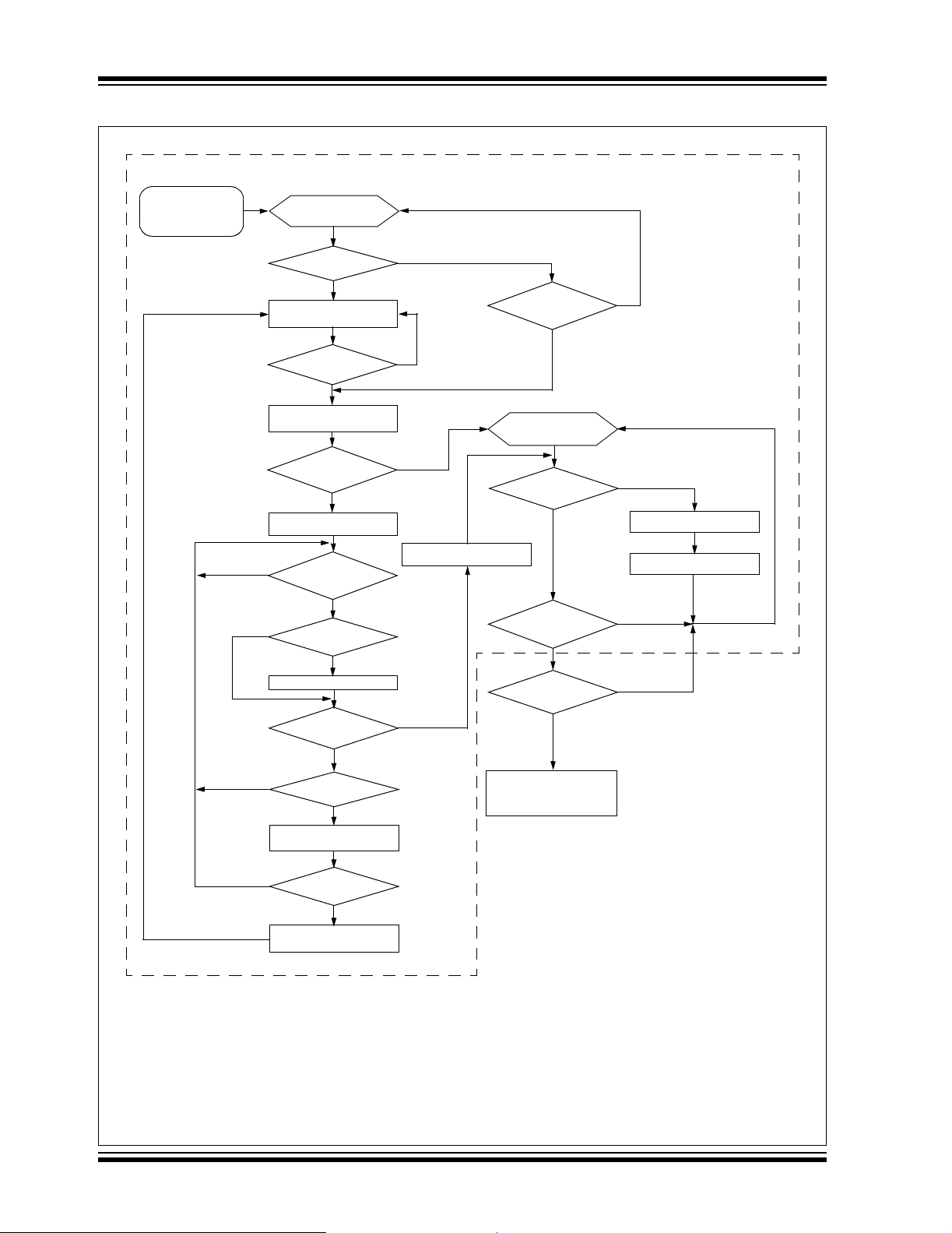
FIGURE 3-3: DISPLAY OPERATION PER DDC STANDARD PROPOSED BY VESA
The 24LC21A was designed to
Display Power-on
or
DDC Circuit Powered
from +5 volts
Communication
is idle
comply to the portion of flowchart insi de das h box
No
No
No
Is Vsync
present?
Yes
Send EDID continuously
using Vsync as clock
High-to-low
transition on
SCL?
Yes
Stop sending EDID.
Switch to DDC2 mode.
Display has
optional
transition state
?
Yes
Set Vsync counter = 0
or start timer
Change on
SCL, SDA or
VCLK lines?
Yes
High - low
transition on SCL
?
Yes
Reset Vsync counter = 0
Valid
DDC2 address
received?
No
VCLK
cycle?
Yes
Increment VCLK counter
(if appropriate)
No
No
No
Reset counter or timer
Yes
High-to-low
transition on
SCL?
Yes
DDC2 communication
idle. Display waiting for
address byte.
DDC2B
address
received?
No
Is display
Access.bus
Valid Access.bus
See Access.bus
specification to determine
correct procedure.
TM
capable?
Yes
address?
Yes
No
Yes
Respond to DDC2B
No
No
Receive DDC2B
command
command
No
Counter=128 or
timer expired?
Yes
Switch back to DDC1
mode.
Note 1: The base flowchart is cop yright 199 3, 1994, 1995 V ideo El ectroni c Standard Ass ociation (VESA) from
VESA’s Display Data Channel (DDC) Standard Proposal ver. 2p rev. 0, used by permission of VESA.
2: The dash box and text “The 24LC21A and... inside dash box.” are added by Microchip Technology Inc.
3: Vsync signal is normally used to derive a signal for VCLK pin on the 24LC21A.
DS21160F-page 6 2003 Microchip Technology Inc.
Page 7
24LC21A
3.1 Bidirectional Mode Bus
Characteristics
The following bus protocol has been defined:
• Data transfer may be initiated only when the bus
is not busy.
• During data transfer, the data line must remain
stable wheneve r the c lock lin e is high . Changes i n
the data line while the clock line is high will be
interpreted as a Start or Stop condition.
Accordingly, the following bus conditions have been
defined (Figure 3-4).
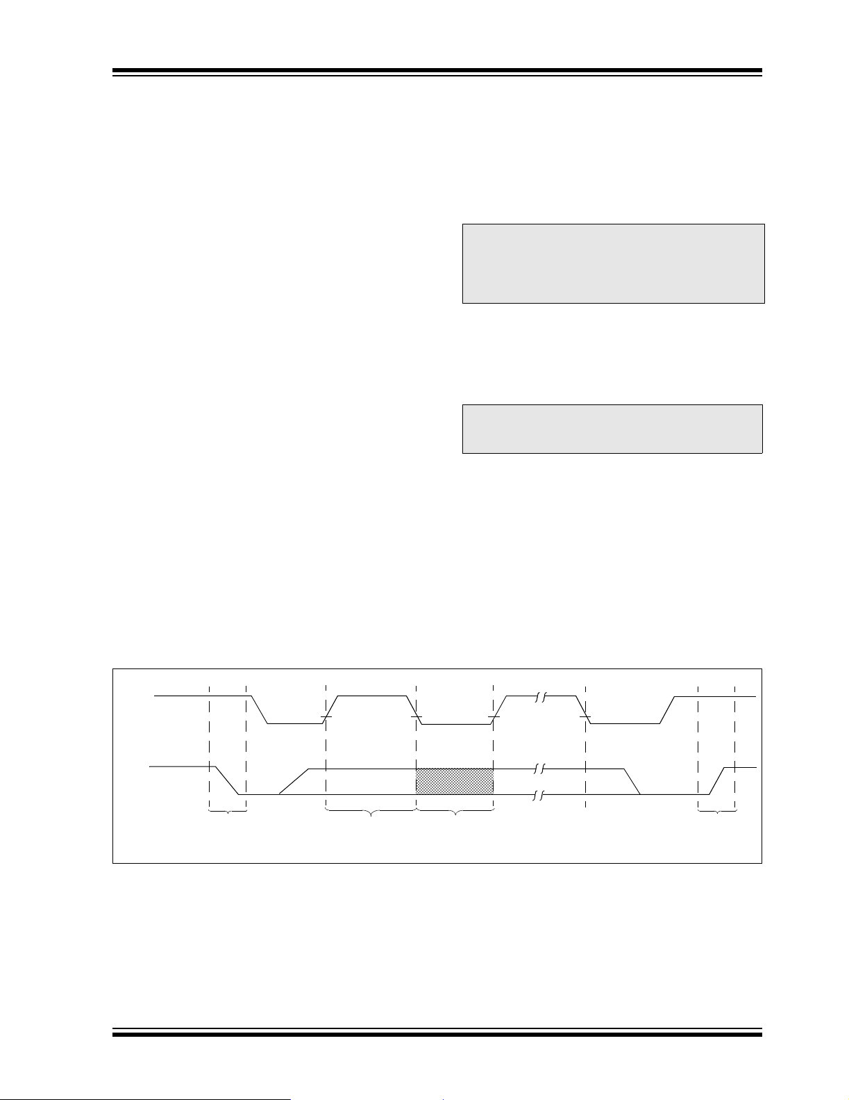
3.1.1 BUS NOT BUSY (A)
Both data and clock lines remain high.
3.1.2 START DATA TRANSFER (B)
A high-to-low transition of the SDA line while the clock
(SCL) is high determines a Start condition. All
commands must be preceded by a Start condition.
3.1.3 STOP DATA TRANSFER (C)
A low-to-high transition of the SDA line while the clock
(SCL) is high determines a Stop condition. All
operations must be ended with a Stop condition.
3.1.4 DATA VALID (D)
The state of the data line represents valid data when,
after a Start condition, the data line is stable for the
duration of the high pe riod of the clock signal.
The data on the line must be changed during the low
period of the clock signa l. Ther e is one cloc k puls e per
bit of data.
Each data transfer is initiated with a S tart condition and
terminated with a Stop condition. The number of the
data bytes transferred between the Start and Stop
conditions is determined by the master device and is
theoretically unlimited, although only the last eight will
be stored when doing a write operation. When an
overwrite does occur it will replace dat a i n a firs t in firs t
out fashion.
Note: Once switched into Bidi rectional mode, th e
24LC21A will remain in that mode until
power is remove d. Re mo vi ng po we r i s the
only way to reset the 24LC21A into the
Transmit-only mode.
3.1.5 ACKNOWLEDGE
Each receiving device, when addressed, is obliged to
generate an acknowledge after the reception of each
byte. The ma ster devi ce m ust gener at e an ex tr a cloc k
pulse which is associated with this Acknowledge bit.
Note: The 24LC21A does not generate any
Acknowledge bits if an internal
programming cycle is in progress.
The device that acknowledges has to pull down the
SDA line during the ackn owledge clock pulse in such a
way that the SDA line is stable low during the high
period of the acknowledge related clock pulse. Of
course, setup and hold times must be taken into
account. A master must signal an end of data to the
slave by not gene rati ng an Ac kno w led ge bi t o n th e last
byte that has been clocked out of the slave. In this
case, the slave must leave the data line high to enable
the master to generate the Stop condition.
FIGURE 3-4: DATA TRANSFER SEQUENCE ON THE SERIAL BUS
(A) (B) (D) (D) (A)(C)
SCL
SDA
START
CONDITION
2003 Microchip Technology Inc. DS21160F-page 7
ADDRESS OR
ACKNOWLEDGE
VALID
DATA
ALLOWED
TO CHANGE
STOP
CONDITION
Page 8
24LC21A
FIGURE 3-5: BUS TIMING START/STOP
SCL
TSU:STA
SDA
START STOP
THD:STA
FIGURE 3-6: BUS TIMING DATA
TF
TLOW
SCL
T
SU:STA
THD:STA
SDA
IN
SDA
OUT
TSP
TAA
THIGH
THD:DAT
TAA
VHYS
TSU:DAT
TSU:STO
TR
TSU:STO
TBUF
3.1.6 SLAVE ADDRESS
After generating a Start condition, the bus master
transmits the s lave addre ss co nsis ting of a 7 -bit dev ice
code (1010000) for the 24LC21A.
The eighth bit of slav e address de termines whether the
master device wants to read or write to the 24LC21A
(Figure 3-7).
The 24LC21A monitors the bus for its corresponding
slave address continuously. It generates an
Acknowledg e bi t if the sl av e ad d r es s was tru e an d i t is
not in a programming mode.
Operation Slave Address R/W
Read 1010000 1
Write 1010000 0
FIGURE 3-7: CONTROL BYTE
ALLOCATION
START
SLAVE ADDRESS
1010000
READ/WRITE
R/W A
DS21160F-page 8 2003 Microchip Technology Inc.
Page 9

24LC21A
4.0 WRITE OPERATION
4.1 Byte Write
Following the start signal from the master, the slave
address (four bits), th ree zero bits (00 0) and the R/W
which is a logic low are placed onto the bus by the
master transmitter. This indicates to the addressed
slave receiver that a byte with a word address will
follow after it has generated an Acknowled ge bit during
the ninth clock cycle. Therefore, the next byte
transmitte d by th e maste r is the word ad dr ess and w ill
be written into the address pointer of the 24LC21A.
After receiving another acknowledge signal from the
24LC21A the master device will transmit the data word
to be written into the addressed memory location. The
24LC21A acknowledges again and the master
generates a Stop condition. This initiates the internal
write cycle, and during this time the 24LC21A will not
generate acknowledge signals (Figure4-1).
It is required that VCLK be held at a logic high level
during command and data transfer in order to program
the device. This applies to both byte write and page
write operation. Note, however, that the VCLK is
ignored during the self-timed program operation.
Changing VCLK from high-to-low during the self-timed
program operation will not
device.
halt programming of the
bit
4.2 Page Write
The write control byte, word address and the first data
byte are transmitted to the 24LC21A in the same way
as in a byte write. But instead of generating a Stop
condition the mast er tran smit s up to eigh t dat a byt es to
the 24LC21A which are temporarily stored in the onchip page buffer and will be written into the memory
after the master has transmit ted a Stop conditi on. After
the receipt of eac h word, the th ree low er ord er addr ess
pointer bits are internally incremented by one. The
higher order five bits of the word address remains
constant. If t he ma ste r should transmit more than eight
words prior to generating the Stop condition, the
address counter will roll over and the previously
received data will be overwri tten. As w ith the by te writ e
operation, once the Stop condition is received an
internal write cycle will begin (Figure 4-3).
It is required that VCLK be held at a logic high level
during command and data transfer in order to program
the device. This applies to both byte write and page
write operation. Note, however, that the VCLK is
ignored during the self-timed program operation.
Changing VCLK from high-to-low during the self-timed
program operation will not
device.
Note: Page write operatio ns are lim ited to wri ting
bytes within a single physical page,
regardless of the numb er o f by tes ac tua ll y
being written. Physical page boundaries
start at addresses that are integer multiples of the page buffe r size ( or ‘page size’)
and end at addresses that are integer
multiples of [page size - 1]. If a Page Write
command attempts to write across a
physical page boundary, the result is that
the data wraps around to the beginning of
the current page (overwriting data
previously stored there), instead of being
written to the next page as might be
expected. It is therefore necessary for the
application software to prevent page write
operations that would attempt to cross a
page boundary.
halt programming of the
2003 Microchip Technology Inc. DS21160F-page 9
Page 10
24LC21A
FIGURE 4-1: BYTE WRITE
BUS ACTIVITY
MASTER
S
T
A
R
T
CONTROL
BYTE
WORD
ADDRESS
DATA
S
T
O
P
SDA LINE
BUS ACTIVITY
VCLK
SP
FIGURE 4-2: VCLK WRITE ENABLE TIMING
SCL
T
SDA
HD:STA THD:STO
IN
VCLK
TVHST
FIGURE 4-3: PAGE WRITE
S
BUS ACTIVITY
MASTER
SDA LINE
T
A
R
T
S
CONTROL
BYTE
WORD
ADDRESS
A
C
K
DATA (n)
A
C
K
DATA n + 1
TSPVL
A
C
K
DATA n + 7
S
T
O
P
P
BUS ACTIVITY
VCLK
A
C
K
A
C
K
A
C
K
A
C
K
A
C
K
DS21160F-page 10 2003 Microchip Technology Inc.
Page 11
24LC21A
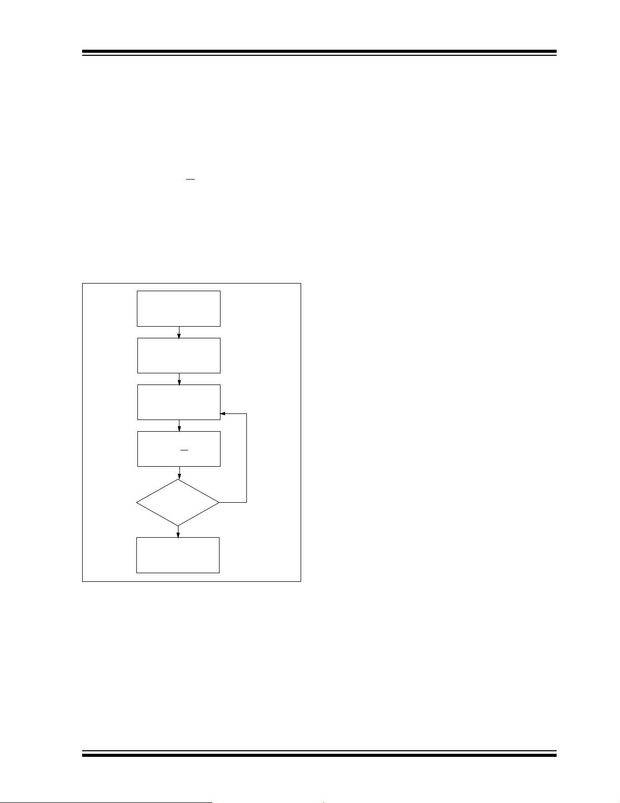
5.0 ACKNOWLEDGE POLLING
Since the device will not acknowledge during a write
cycle, this can be used to determine when the cycle is
complete (this feature can be used to maximize bus
throughput). Once the Stop condition for a Write
command has been issu ed from the mas ter , the device
initiates the internally timed write cycle. ACK polling
can be initiated immediately. This involves the master
sending a Start condition followed by the control byte
for a Write command (R/W
busy with the write cycle, then no ACK will be returned.
If the cycle is complete, then the device will return the
ACK and the master can then proceed with the next
Read or Write command. See Figure 5-1 for the flow
diagram.
FIGURE 5-1: ACKNOWLEDGE
Write Command
Send Stop
Condition to
Initiate Write Cycl e
= 0). If the device is still
POLLING FLOW
Send
6.0 WRITE PROTECTION
When using the 24LC 21A in the Bidirecti onal mode, the
VCLK pin can be used as a write-protect control pin.
Setting VCLK high allows normal write operations,
while setting VCLK low prevent s w riting to any locatio n
in the array. Connecting the VCLK pin to VSS would
allow the 24LC21A to operate as a serial ROM,
although this configuration would prevent using the
device in the Transmit-only mode.
Send Start
Send Control Byte
with R/W
Acknowledge
(ACK = 0)?
= 0
Did Device
Yes
Next
Operation
No
2003 Microchip Technology Inc. DS21160F-page 11
Page 12

24LC21A
7.0 READ OPERATION
Read operations are initiated in the same way as write
operations with the exception that the R/W
slave address is set to one. The re are three ba sic types
of read operations: current add ress read , rand om rea d
and sequential read.
7.1 Current Address Read
The 24LC21A contains an address counter that
maintains the address of the last word accessed,
internally incremented by one. Therefore, if the
previous access (either a read or write operation) was
to address n, the next current address read operation
would access d at a from address n + 1. U pon rec ei pt of
the slave address wit h R/W
issues an acknowl edg e and transm it s the eight bit dat a
word. The master will n ot acknow ledg e the tra nsfer but
does generate a Stop condition and the 24LC21A
discontinues transmission (Figure 7-1).
FIGURE 7-1: CURRENT ADDRESS
S
BUS ACTIVITY
MASTER
SDA LINE
BUS ACTIVITY
T
A
R
T
SP
bit set to one, the 24LC21A
READ
CONTROL
BYTE
101
0000
1
A
C
K
DATA n
bit of the
S
T
O
P
N
O
A
C
K
7.3 Sequential Read
Sequential reads are initiated in the same way as a
random read except that after the 24LC21A transmits
the first data byte, the master issues an acknowledge
as opposed to a Stop condition in a random read. This
directs the 24LC21A to transmit the next sequentially
addressed 8-bit word (Figure 7-3).
To provide sequential reads the 24LC21A contains an
internal address poin ter which is i ncremented by o ne at
the completion of ea ch operation. This a ddre ss po inter
allows the entire memory contents to be serially read
during one operation.
7.4 Noise Protection
The 24LC21A emp loys a VCC threshold detector circuit
which disables the internal erase/write logic if the V
is below 1.5 volts at nominal conditions.
The SDA, SCL and VCLK inputs have Schmitt Trigger
and filter circuit s which suppres s noise spike s to assure
proper device operation even on a noisy bus.
CC
7.2 Random Read
Random read operations allow the master to access
any memory location in a random manner. To perform
this type of read operatio n, fi rst the word address must
be set. This is d one by sending the word a ddress to the
24LC21A as part of a write operation. After the word
address is sent, the master gen erates a Start cond ition
following the acknowledge. This terminates the write
operation, but not before the internal add ress pointe r is
set. Then the master issues the control byte again but
with the R/W
issue an acknowledge and transmits the 8-bit data
word. The master will n ot acknow ledg e the tra nsfer but
does generate a Stop condition and the 24LC21A
discontinues transmission (Figure 7-2).
bit set to a one. The 24LC21A will then
DS21160F-page 12 2003 Microchip Technology Inc.
Page 13

FIGURE 7-2: RANDOM READ
S
T
BUS ACTIVITY
MASTER
SDA LINE
BUS ACTIVITY
A
CONTROL
R
T
SSTP
BYTE
10100000 00000111
A
C
K
FIGURE 7-3: SEQUENTIAL READ
BUS ACTIVITY
MASTER
CONTROL
BYTE
SDA LINE
BUS ACTIVITY
DATA n DATA n+1
A
C
K
A
C
K
WORD
ADDRESS
24LC21A
S
T
A
CONTROL
R
A
C
K
A
C
K
BYTE
DATA n+2 DATA n+X
A
C
K
DATA n
A
C
K
S
T
O
P
N
O
A
C
K
S
T
O
P
P
N
O
A
C
K
2003 Microchip Technology Inc. DS21160F-page 13
Page 14

24LC21A
8.0 PIN DESCRIPTIONS
8.1 SDA
This pin is use d to transfer addresses and data into and
out of the device , when the dev ice is in th e Bidirectiona l
mode. In the Transmit-only mode, which only allows
data to be read from the device, dat a is also tr ansferred
on the SDA pin. This pin is an open drain terminal,
therefore the SDA bus requires a pull-up resistor to
CC (typical 10 KΩ for 100 kHz, 2 KΩ for 400 kHz).
V
For normal data tr ansfer in the Bidirecti onal mode, SDA
is allowed to change only during SCL low. Changes
during SCL high are reserved for indicating the Start
and Stop conditions.
8.2 SCL
This pin is the clock input for the Bidirectional mode,
and is used to sy nchronize dat a transfer to a nd from the
device. It is also used as the signaling input to switch
the device from the Transmit-only mode to the
Bidirectional mode. It must remain high for the chip to
continue operation in the Transmit-only mode.
8.3 VCLK
This pin is the clock input for the Transmit-only mode
(DDC1). In the Transmit-only mode, each bit is clocked
out on the rising edge of this s ignal. In the Bidire ctiona l
mode, a high log ic level is req uired on t his pin to en able
write capability.
DS21160F-page 14 2003 Microchip Technology Inc.
Page 15

APPENDIX A: REVISION HISTORY
Revision F
Corrections to Section 1.0, Electrical Characteristics.
24LC21A
2003 Microchip Technology Inc. DS21160F-page 15
Page 16

24LC21A
PRODUCT IDENTIFICATION SYSTEM
To order or obtain information, e.g., on pricing or delivery , refer to the factory or the listed sales office.
PART NO. X /XX XXX
Device
Device 24LC21A Dual Mode Serial EEPROM
Temperature Range Blank 0°C to +70°C
Package P = Plastic DIP (300 mil Body), 8-lead
Range
24LC21AT Dual Mode Serial EEPROM (Tape and Reel)
I -40°C to +85°C
SN = Plastic SOIC (150 mil Body), 8-lead
PatternPackageTemperature
Sales and Support
Data Sheets
Products supported by a preliminary Data Sheet may have an errata sheet describing minor operational differences and
recommended workarounds. To determine if an errata sheet exists for a particular device, please contact one of the following:
1. Your local Microchip sales office
2. The Microchip Corporate Literature Center U.S. FAX: (480) 792-7277
3. The Microchip Worldwide Site (www.microchip.com)
Please specify which device, revision of silicon and Data Sheet (include Literature #) you are using.
New Customer Notification System
Register on our web site (www.microchip.com/cn) to receive the most current information on our products.
DS21160F-page 16 2003 Microchip Technology Inc.
Page 17
Note the following details of the code protection feature on Microchip devices:
• Microchip products meet the specification contained in their particular Microchip Data Sheet.
• Microchip believes that its family of products is one of the most secure families of its kind on the market today, when used in the
intended manner and under normal conditions.
• There are dishonest and possibly illegal methods used to breach the code protection feature. All of these methods, to our
knowledge, require using the Microchip products in a manner outside the operating specifications contained in Microchip's Data
Sheets. Most likely, the person doing so is engaged in theft of intellectual property.
• Microchip is willing to work with the customer who is concerned about the integrity of their code.
• Neither Microchip nor any other semiconductor manufacturer can guarantee the security of their code. Code protection does not
mean that we are guaranteeing the product as “unbreakable.”
Code protection is constantly evolving. We at Microchip are committed to continuously improving the code protection features of our
products. Attempts to break microchip’s code protection feature may be a violation of the Digital Millennium Copyright Act. If such acts
allow unauthorized access to your software or other copyrighted work, you may have a right to sue for relief under that Act.
Information contained in this publication regarding device
applications and the like is intended through suggestion only
and may be superseded by updates. It is your responsibility to
ensure that your application meets with your specifications.
No representation or warranty is given and no liability is
assumed by Microchip Technology Incorporated with respect
to the accuracy or use of such information, or infringement of
patents or other intellectual property rights arising from such
use or otherwise. Use of Microchip’s products as critical components in life support systems is not authorized except with
express written approval by Microchip. No licenses are conveyed, implicitly or otherwise, under any intellectual property
rights.
Trademarks
The Microchip name and logo, the Microchip logo, Accuron,
dsPIC, K
EELOQ, MPLAB, PIC, PICmic ro, PI C START,
PRO MATE and PowerSmart are registered trademarks of
Microchip Technology Incorporated in the U.S.A. and other
countries.
AmpLab, FilterLab, microID, MXDEV, MXLAB, PICMASTER,
SEEVAL and The Embedded Control Solutions Company are
registered trademarks of Microchip Technology Incorporated
in the U.S.A.
Application Maestro, dsPICDEM, dsPICDEM.net, ECAN,
ECONOMONITOR, FanSense, FlexROM, fuzzyLAB,
In-Circuit Serial Programming, ICSP, ICEPIC, microPort,
Migratable Memory, MPASM, MPLIB, MPLINK, MPSIM,
PICkit, PICDEM, PICDEM.net, PowerCal, PowerInfo,
PowerMate, PowerTool, rfLAB, rfPIC, Select Mode,
SmartSensor, SmartShunt, SmartT el and Total Endurance are
trademarks of Microchip Technology Incorporated in the
U.S.A. and other countries.
Serialized Quick Turn Programming (SQTP) is a service mark
of Microchip Technology Incorporated in the U.S.A.
All other trademarks mentioned herein are property of their
respective companies.
© 2003, Microchip Technology Incorporated, Printed in the
U.S.A., All Rights Reserved.
Printed on recycled paper.
Microchip received QS-9000 quality system
certification for its worldwide headquarters,
design and wafer fabrication facilities in
Chandler and Tempe, Arizona in July 1999
and Mountain View, California in March 2002.
The Company’s quality system processes and
procedures are QS-9000 compliant for its
PICmicro
devices, Serial EEPROMs, microperipherals,
non-volatile memory and analog products. In
addition, Microchip’s quality system for the
design and manufacture of development
systems is ISO 9001 certified.
®
8-bit MCUs, KEELOQ
®
code hopping
2003 Microchip Technology Inc. DS21160F-page 17
Page 18

WORLDWIDE SALES AND SERVICE
AMERICAS
Corporate Office
2355 West Chandler Blvd.
Chandler, AZ 85224-6199
Tel: 480-792-7200
Fax: 480-792-7277
Technical Support: 480-792-7627
Web Address: http://www.microchip.com
Atlanta
3780 Mansell Road, Suite 130
Alpharetta, GA 30022
Tel: 770-640-0034
Fax: 770-640-0307
Boston
2 Lan Drive, Suite 120
Westford, MA 01886
Tel: 978-692-3848
Fax: 978-692-3821
Chicago
333 Pierce Road, Suite 180
Itasca, IL 60143
Tel: 630-285-0071
Fax: 630-285-0075
Dallas
4570 Westgrove Drive, Suite 160
Addison, TX 75001
Tel: 972-818-7423
Fax: 972-818-2924
Detroit
Tri-Atria Office Building
32255 Northwestern Highway, Suite 190
Farmington Hills, MI 48334
Tel: 248-538-2250
Fax: 248-538-2260
Kokomo
2767 S. Albright Road
Kokomo, IN 46902
Tel: 765-864-8360
Fax: 765-864-8387
Los Angeles
18201 Von Karman, Suite 1090
Irvine, CA 92612
Tel: 949-263-1888
Fax: 949-263-1338
Phoenix
2355 West Chandler Blvd.
Chandler, AZ 85224-6199
Tel: 480-792-7966
Fax: 480-792-4338
San Jose
2107 North First Street, Suite 590
San Jose, CA 95131
Tel: 408-436-7950
Fax: 408-436-7955
Toronto
6285 Northam Drive, Suite 108
Mississauga, Ontario L4V 1X5, Cana da
Tel: 905-673-0699
Fax: 905-673-6509
ASIA/PACIFIC
Australia
Suite 22, 41 Rawson Street
Epping 2121, NSW
Australia
Tel: 61-2-9868-6733
Fax: 61-2-9868-6755
China - Beijing
Unit 915
Bei Hai Wan Tai Bldg.
No. 6 Chaoyangmen Beidajie
Beijing, 100027, No. China
Tel: 86-10-85282100
Fax: 86-10-85282104
China - Chengdu
Rm. 2401-2402, 24th Floor,
Ming Xing Financial Tower
No. 88 TIDU Street
Chengdu 610016, China
Tel: 86-28-86766200
Fax: 86-28-86766599
China - Fuzhou
Unit 28F, World Trade Plaza
No. 71 Wusi Road
Fuzhou 350001, China
Tel: 86-591-7503506
Fax: 86-591-7503521
China - Hong Kong SAR
Unit 901-6, Tower 2, Metroplaza
223 Hing Fong Road
Kwai Fong, N.T., Hong Kong
Tel: 852-2401-1200
Fax: 852-2401-3431
China - Shanghai
Room 701, Bldg. B
Far East International Plaza
No. 317 Xian Xia Road
Shanghai, 200051
Tel: 86-21-6275-5700
Fax: 86-21-6275-5060
China - Shenzhen
Rm. 1812, 18/F, Building A, United Plaza
No. 5022 Binhe Road, Futian District
Shenzhen 518033, China
Tel: 86-755-82901380
Fax: 86-755-8295-1393
China - Shunde
Room 401, Hongjian Building
No. 2 Fengxiangnan Road, Ronggui Town
Shunde City, Guangdong 528303, China
Tel: 86-765-8395507 Fax: 86-765-8395571
China - Qingdao
Rm. B505A, Fullhope Plaza,
No. 12 Hong Kong Central Rd.
Qingdao 266071, China
Tel: 86-532-5027355 Fax: 86-532-5027205
India
Divyasree Chambers
1 Floor, Wing A (A3/A4)
No. 11, O’Shaugnessey Road
Bangalore, 560 025, India
Tel: 91-80-2290061 Fax: 91-80-2290062
Japan
Benex S-1 6F
3-18-20, Shinyokohama
Kohoku-Ku, Yokohama-shi
Kanagawa, 222-0033, Japan
Tel: 81-45-471- 6166 Fax: 81-45-4 71 -61 22
Korea
168-1, Youngbo Bldg. 3 Floor
Samsung-Dong, Kangnam-Ku
Seoul, Korea 135-882
Tel: 82-2-554-7200 Fax: 82-2-558-5932 or
82-2-558-5934
Singapore
200 Middle Road
#07-02 Prime Centre
Singapore, 188980
Tel: 65-6334-8870 Fax: 65-6334-8850
Taiwan
Kaohsiung Branch
30F - 1 No. 8
Min Chuan 2nd Road
Kaohsiung 806, Taiwan
Tel: 886-7-536-4818
Fax: 886-7-536-4803
Taiwan
Taiwan Branch
11F-3, No. 207
Tung Hua North Road
Taipei, 105, Taiwan
Tel: 886-2-2717-7175 Fax: 886-2-2545-0139
EUROPE
Austria
Durisolstrasse 2
A-4600 Wels
Austria
Tel: 43-7242-2244-399
Fax: 43-7242-2244-393
Denmark
Regus Business Centre
Lautrup hoj 1-3
Ballerup DK-2750 Denmark
Tel: 45-4420-9895 Fax: 45-4420-9910
France
Parc d’Activite du Moulin de Massy
43 Rue du Saule Trapu
Batiment A - ler Etage
91300 Massy, France
Tel: 33-1-69-53-63-20
Fax: 33-1-69-30-90-79
Germany
Steinheilstrasse 10
D-85737 Ismaning, Germany
Tel: 49-89-627-144-0
Fax: 49-89-627-144-44
Italy
Via Quasimodo, 12
20025 Legnano (MI)
Milan, Italy
Tel: 39-0331-742611
Fax: 39-0331-466781
Netherlands
P. A. De Biesbosch 14
NL-5152 SC Drunen, Netherlands
Tel: 31-416-690399
Fax: 31-416-690340
United Kingdom
505 Eskdale Road
Winnersh Triangle
Wokingham
Berkshir e, England RG41 5TU
Tel: 44-118-921-5869
Fax: 44-118-921-5820
07/28/03
DS21160F-page 18 2003 Microchip Technology Inc.
 Loading...