

24AA1025/24LC1025/24FC1025
1024K I2C™ CMOS Serial EEPROM
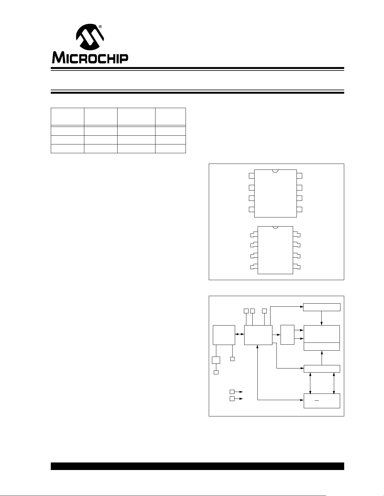
Device Selection Table:
Part
Number
24AA1025 1.7-5.5V 400 kHz
24LC1025 2.5-5.5V 400 kHz* I, E
24FC1025 2.5-5.5V 1 MHz I
†
100 kHz for VCC < 2.5V.
*100 kHz for V
VCC
Range
CC < 4.5V, E-temp.
Max. Clock
Frequency
†
Temp
Ranges
I
Features:
• Single supply with operation down to 1.7V for
24AAXX devices, 2.5V for 24LCXX devices
• Low-power CMOS technology:
- Read current 1 mA, typical
- Standby current 100 nA, typical
• 2-wire serial interface, I2C™ compatible
• Cascadable up to four devices
• Schmitt Trigger inputs for noise suppression
• Output slope control to eliminate ground bounce
• 100 kHz and 400 kHz clock compatibility
• 1 MHz clock for FC versions
• Page write time 3 ms, typical
• Self-timed erase/write cycle
• 128-byte page write buffer
• Hardware write-protect
• ESD protection >400 V
• More than 1 million erase/write cycles
• Data retention >200 years
• Factory programming available
• Packages include 8-lead PDIP, SOIJ
• Pb-free and RoHS compliant
• Temperature ranges:
- Industrial (I): -40°C to +85°C
- Automotive (E):-40°C to +125°C
This device is capable of both random and sequential
reads. Reads may b e sequential within addres s boundaries 0000h to FFFFh and 10000h to 1FFFFh.
Functional addre ss lines allow up t o four de vices on the
same data bus. This allows for up to 4 Mbits total
system EEPROM memory. This device is available in
the standard 8-pin PDIP and SOIJ packages.
Package Type
PDIP
SOIJ
A0
1
A1
2
A2
3
V
SS
4
1
A0
2
A1
3
A2
4
SS
V
VCC
8
WP
7
SCL
6
SDA
5
8
V
CC
7
WP
6
SCL
5
SDA
Block Diagram
A0A1
Control
I/O
SDA
I/O
Logic
SCL
WP
Memory
Control
Logic
XDEC
HV Generator
EEPROM
Array
Page Latches
YDEC
V
Description:
The Microchip Technology Inc. 24AA1025/24LC1025/
VSS
CC
Sense AMP
Control
R/W
24FC1025 (24XX1025*) is a 128K x 8 (1024K bit)
Serial Ele ctrically E rasable PROM, capable of op eration across a broad vo lta ge range (1.8V to 5 .5V). It has
been developed for advanced, low-power applications
such as personal communications or data acquisition.
This device has both byte write and page write
capability of up to 128 bytes of data.
© 2007 Microchip Technology Inc. Preliminary DS21941E-page 1
*24XX1025 is used in this document as a generic part number
for the 24AA1025/24LC1025/24FC1025 devices.
24AA1025/24LC1025/24FC1025
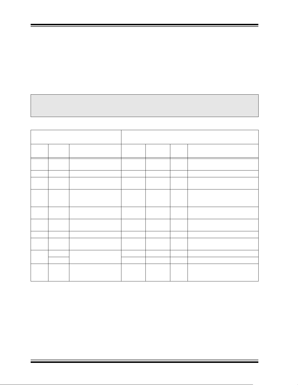
1.0 ELECTRICAL CHARACTERISTICS
Absolute Maximum Ratings
(†)
VCC.............................................................................................................................................................................6.5V
All inputs and outputs w.r.t. V
SS .........................................................................................................-0.6V to VCC +1.0V
Storage temperature ...............................................................................................................................-65°C to +150°C
Ambient temperature with power applied................................................................................................-40°C to +125°C
ESD protection on all pins ......................................................................................................................................................≥ 4kV
† NOTICE: Stresses above those listed under “Absolute Maximum Ratings” may cause permanent damage to the
device. This is a stres s ratin g only and func tional operati on of the devic e at thos e or any other co nditio ns abov e thos e
indicated in the operational listings of this specification is not implied. Exposure to maximum rating conditions for
extended periods may affect device reliability.
TABLE 1-1: DC CHARACTERISTICS
DC CHARACTERISTICS
Param.
No.
Sym. Characteristic Min. Max. Units Conditions
D1 A0, A1, SCL, SDA and
Industrial (I): V
Automotive (E): V
———
WP pins:
D2 V
IH High-level input voltage 0.7 VCC —V
D3 VIL Low-level input voltage — 0.3 VCC
D4 V
HYS Hysteresis of Schmitt
CC —VVCC ≥ 2.5V (Note)
0.05 V
Trigger inputs
(SDA, SCL pins)
D5 VOL Low-level output voltage — 0.40 V IOL = 3.0 mA @ VCC = 4.5V
D6 ILI Input leakage current — ±1 μAVIN = VSS or VCC, WP = VSS
D7 ILO Output leakage current — ±1 μAVOUT = VSS or VCC
D8 CIN,
C
OUT
Pin capacitance
(all inputs/outpu t s)
—10pFVCC = 5.0V (Note)
D9 ICC Read Operating current — 450 μAVCC = 5.5V, SCL = 400kHz
ICC Write — 5 mA VCC = 5.5V
D10 I
CCS Standby current — 5
Note: This parameter is periodically sampled and not 100% tested.
CC = +1.7V to 5.5V TA = -40°C to +85°C
CC = +2.5V to 5.5VTA = -40°C to +125°C
VVVCC ≥ 2.5V
0.2 VCC
CC < 2.5V
V
OL = 2.1 mA @ VCC = 2.5V
I
VIN = VSS or VCC, WP = VCC
T
A = 25°C, FCLK = 1 MHz
μATA = -40°C to 85°C
SCL = SDA = V
A0, A1, WP = V
CC = 5.5V
SS, A2 = VCC
DS21941E-page 2 Preliminary © 2007 Microchip Technology Inc.

24AA1025/24LC1025/24FC1025
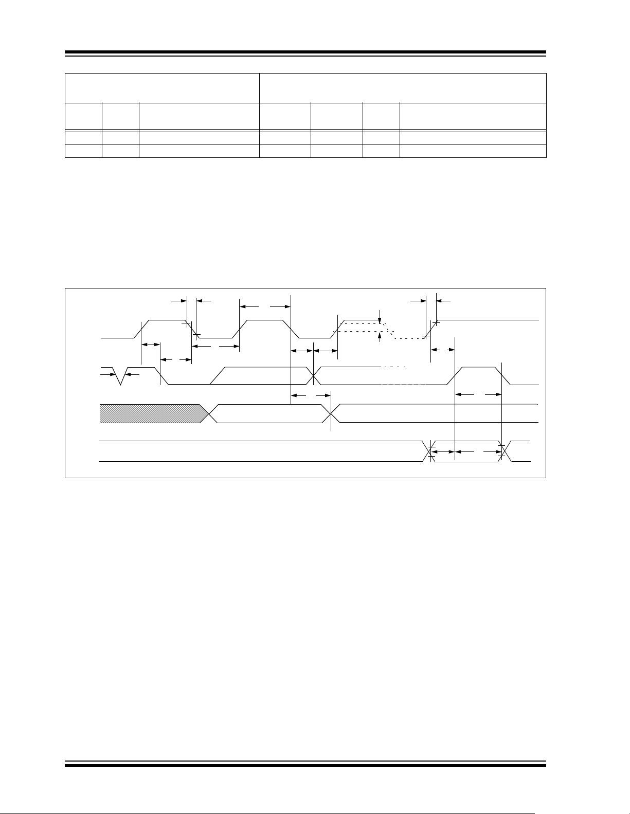
TABLE 1-2: AC CHARACTERISTICS
AC CHARACTERISTICS
Param.
No.
1F
2T
3T
4T
5T
6T
7T
8T
9T
10 T
11 T
12 T
13 T
14 T
15 T
16 T
Note 1: Not 100% tested. C
Sym. Characteristic Min. Max. Units Conditions
CLK Clock frequency —
HIGH Clock high time 4000
LOW Clock low time 4700
R SDA and SCL rise time
(Note 1)
F SDA and SCL fall time
(Note 1)
HD:STA Start condition hold time 4000
SU:STA Start condition setup time 4700
HD:DAT Data input hold time 0 — ns (Note 2)
SU:DAT Data input setup time 250
SU:STO Stop condition setup time 4000
SU:WP WP setup time 4000
HD:WP WP hold time 4700
AA Output valid from clock
(Note 2)
BUF Bus free time: Time the bus
must be free before a new
transmission can start
OF Output fall time from VIH
minimum to VIL maximum
B ≤ 100 pF
C
SP Input filter spike suppression
(SDA and SCL pins)
2: As a transmitter, the device must provide an internal minimum delay time to bridge the undefined region (minimum
300 ns) of the falling edge of SCL to avoid unintended generation of Start or Stop conditions.
3: The combine d T
suppression. This eliminates the need for a TI specification for standard operation.
4: This parameter is not tested but established by characterization. For endurance e stimates in a specific application,
please consult the Total Endurance™ Model which can be obtained from Microchip’s web site at www.microchip.com.
5: Max. clock frequency is 100 kHz for E-temp devices <4.5V. 1.7-2.5V (100 kHz) timings must be used.
Industrial (I): V
Automotive (E): V
—
—
600
500
1300
500
—
—
—
—
—
600
250
600
250
100
100
600
250
600
600
1300
1300
—
—
—
4700
1300
500
10 + 0.1C
CC = +1.7V to 5.5V TA = -40°C to +85°C
CC = +2.5V to 5.5V TA = -40°C to +125°C
100
400
1000
—
—
—
—
—
—
1000
300
300
300
100
—
—
—
—
—
—
—
—
—
—
—
—
—
—
—
—
—
—
3500
900
400
—
—
—
B 250
250
kHz 1.7V ≤ VCC ≤ 2.5V
2.5V ≤ V
2.5V ≤ V
CC ≤ 5.5V (Note 5)
CC ≤ 5.5V (24FC1025 only)
ns 1.7V ≤ VCC ≤ 2.5V
2.5V ≤ V
2.5V ≤ V
CC ≤ 5.5V
CC ≤ 5.5V (24FC1025 only)
ns 1.7V ≤ VCC ≤ 2.5V
2.5V ≤ V
2.5V ≤ V
CC ≤ 5.5V
CC ≤ 5.5V (24FC1025 only)
ns 1.7V ≤ VCC ≤ 2.5V
2.5V ≤ V
2.5V ≤ V
CC ≤ 5.5V
CC ≤ 5.5V (24FC1025 only)
ns All except, 24FC1025
2.5V ≤ V
CC ≤ 5.5V (24FC1025 only)
ns 1.7V ≤ VCC ≤ 2.5V
2.5V ≤ V
2.5V ≤ V
CC ≤ 5.5V
CC ≤ 5.5V (24FC1025 only)
ns 1.7V ≤ VCC ≤ 2.5V
2.5V ≤ V
2.5V ≤ V
CC ≤ 5.5V
CC ≤ 5.5V (24FC1025 only)
ns 1.7V ≤ VCC ≤ 2.5V
2.5V ≤ V
2.5V ≤ V
CC ≤ 5.5V
CC ≤ 5.5V (24FC1025 only)
ns 1.7V ≤ VCC ≤ 2.5V
2.5V ≤ V
2.5V ≤ V
CC ≤ 5.5V
CC ≤ 5.5V (24FC1025 only)
ns 1.7V ≤ VCC ≤ 2.5V
2.5V ≤ V
2.5V ≤ V
CC ≤ 5.5V
CC ≤ 5.5V (24FC1025 only)
ns 1.7V ≤ VCC ≤ 2.5V
2.5V ≤ V
2.5V ≤ V
CC ≤ 5.5V
CC ≤ 5.5V (24FC1025 only)
ns 1.7V ≤ VCC ≤ 2.5V
2.5V ≤ V
2.5V ≤ V
CC ≤ 5.5V
CC ≤ 5.5V (24FC1025 only)
ns 1.7V ≤ VCC ≤ 2.5V
2.5V ≤ V
2.5V ≤ V
CC ≤ 5.5V
CC ≤ 5.5V (24FC1025 only)
ns All except, 24FC1025 (Note 1)
24FC1025 (Note 1)
— 50 ns All except, 24FC1025 (Notes 1 and 3)
B = total capacitance of one bus line in pF.
SP and VHYS specifications are due to new Schmitt Trigger inputs which provide improved noise spike
© 2007 Microchip Technology Inc. Preliminary DS21941E-page 3
24AA1025/24LC1025/24FC1025
AC CHARACTERISTICS (Continued)
Param.
No.
17 TWC Write cycle time (byte or page) — 5 ms 3 ms, typical
18 Endurance 1 M — cycles 25°C (Note 4)
Note 1: Not 100% tested. C
Sym. Characteristic Min. Max. Units Conditions
B = total capacitance of one bus line in pF.
2: As a transmitter, the device must provide an internal minimum delay time to bridge the undefined region (minimum
300 ns) of the falling edge of SCL to avoid unintended generation of Start or Stop conditions.
3: The combined T
suppression. This eliminates the need for a TI specification for standard operation.
4: This parameter is not tested but established by characterization. For endurance e stimates in a specific application,
please consult the Total Endurance™ Model which can be obtained from Microchip’s web site at www.microchip.com.
5: Max. clock frequency is 100 kHz for E-temp devices <4.5V. 1.7-2.5V (100 kHz) timings must be used.
SP and VHYS specifications are due to new Schmitt Trigger inputs which provide improved noise spike
Industrial (I): V
Automotive (E): V
CC = +1.7V to 5.5V TA = -40°C to +85°C
CC = +2.5V to 5.5V TA = -40°C to +125°C
FIGURE 1-1: BUS TIMING DATA
SCL
SDA
IN
16
5
7
6
3
2
89
D4
4
10
SDA
OUT
WP
13
(protected)
(unprotected)
14
11
12
DS21941E-page 4 Preliminary © 2007 Microchip Technology Inc.
24AA1025/24LC1025/24FC1025
2.0 PIN DESCRIPTIONS
The descriptions of the pins are listed in Table 2-1.
TABLE 2-1: PIN FUNCTION TABLE
Name PDIP SOIJ Function
A0 1 1 User Configurable Chip Select
A1 2 2 User Configurable Chip Select
A2 3 3 Non-Configurable Chip Select.
This pin must be hard-wired to
logical 1 state (V
will not operate with this pin
left floating or held to logical 0
SS).
(V
VSS 4 4 Ground
SDA 5 5 Serial Data
SCL 6 6 Serial Clock
WP 7 7 Write-Protect Input
CC 8 8 +1.7 to 5.5V (24AA1025)
V
+2.5 to 5.5V (24LC1025)
+2.5 to 5.5V (24FC1025)
2.1 A0, A1 Chip Address Inputs
CC). Device
2.4 Serial Clock (SCL)
This input is used to sync hronize the data trans fer from
and to the device.
2.5 Write-Protect (WP)
This pin must be conne cted to eithe r VSS or VCC. If tied
SS, write operations are enabled. If tied to VCC,
to V
write operations are inhibited, but read operations are
not affected.
3.0 FUNCTIONAL DESCRIPTION
The 24XX1025 supports a bidirectional 2-wire bus and
data transmission protocol. A device that sends data
onto the bus is defined as a transmitter and a device
receiving data, as a receiver. The bus must be
controlled by a master device which generates the
Serial Clock (SCL), controls the bus access, and
generates the Start and Stop conditions while the
24XX1025 works as a slave. Both master and slave
can operate as a transmitt er or receive r , but the m aster
device determines which mode is activated.
The A0, A1 inputs are used by the 24XX1025 fo r multiple device operations. The levels on these inputs are
compared with the corresponding bits in the slave
address. The chip is selected if the comparison is true.
Up to four devices may be connected to the same bus
by using differ ent Chip Sele ct bit com binations. In most
applications, the chip address inputs A0 and A1 are
hard-wired to logic ‘0’ or logic ‘1’. For applications in
which thes e pin s ar e c o nt ro ll ed b y a m ic r oc ont r ol l er o r
other programmable device, the chip address pins
must be driven to logic ‘0’ or logic ‘1’ before normal
device operation can proceed.
2.2 A2 Chip Address Input
The A2 input is non-configurable Chip Select. This pin
must be tied to V
CC in order for this device to operate.
2.3 Serial Data (SDA)
This is a bidirectional pin used to transfer addresses
and data into and data out of the device. It is an opendrain terminal, therefore, the SDA bus requires a pullup resistor to V
400kHz and 1MHz).
For normal data t ransfer SDA is all owed to change only
during SCL low. Changes during SCL high are
reserved for indicatin g the Start and Stop conditions.
CC (typical 10 kΩ for 100 kHz, 2 kΩ for
© 2007 Microchip Technology Inc. Preliminary DS21941E-page 5
24AA1025/24LC1025/24FC1025
4.0 BUS CHARACTERISTICS
The following bus protocol has been defined:
• Data transfer may be initiated only when the bus
is not busy.
• During data transfer, the data line must remain
stable wheneve r the c lock lin e is high . Changes i n
the data line while the clock line is high will be
interpreted as a Start or Stop condition.
Accordingly, the following bus conditions have been
defined (Figure 4-1).
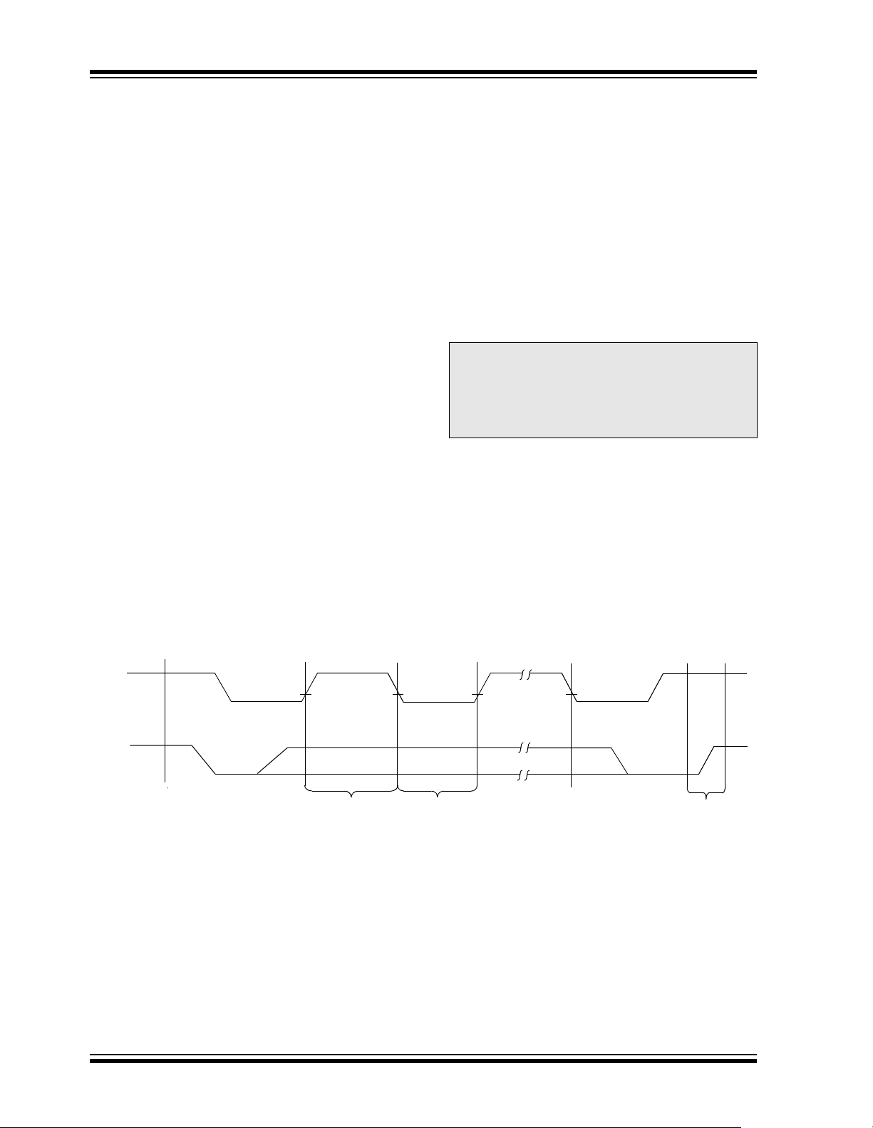
4.1 Bus Not Busy (A)
Both data and clock lines remain high.
4.2 Start Data Transfer (B)
A high-to-low transition of the SDA line while the clock
(SCL) is high determines a Start condition. All
commands must be preceded by a Start condition.
4.3 Stop Data Transfer (C)
A low-to-high transition of the SDA line while the clock
(SCL) is high determines a Stop condition. All
operations must end with a Stop condition.
4.4 Data Valid (D)
The state of the data line represents valid data when,
after a Start condition, the data line is stable for the
duration of the high period of the clock signal.
The data on the line must be changed during the low
period of the clock signal. There is one bit of data per
clock pulse.
Each data transfer is initiated with a S tart condition and
terminated with a Stop condition. The number of the
data bytes transferred between the Start and Stop
conditions is determined by the master device.
4.5 Acknowledge
Each receiving device, when addressed, is obliged to
generate an Acknowledge signal after the reception of
each byte. The master device must generate an extra
clock pulse which is associated with this Acknowledge
bit.
Note: The 24XX1025 does not generate any
Acknowledge bits if an internal programming cycle is in progress, however, the
control byte that is being polled must
match the control byte used to initiate the
write cycle.
A device that acknowledges must pull-down the SDA
line during the Acknowledge clock pulse in such a way
that the SDA line is sta ble low d uring the high pe riod of
the acknowledge related clock pulse. Of course, setup
and hold times must be taken into account. During
reads, a master m ust s ignal an end of dat a to the sl ave
by NOT generating an Acknow ledge bit on the las t byte
that has been cl ocke d out o f the slave . In th is ca se , the
slave (24XX1025) will leave the data line high to enabl e
the master to generate the Stop condition.
FIGURE 4-1: DATA TRANSFER SEQUENCE ON THE SERIAL BUS
FIGURE 4-2: ACKNOWLEDGE TIMING
DS21941E-page 6 Preliminary © 2007 Microchip Technology Inc.
24AA1025/24LC1025/24FC1025
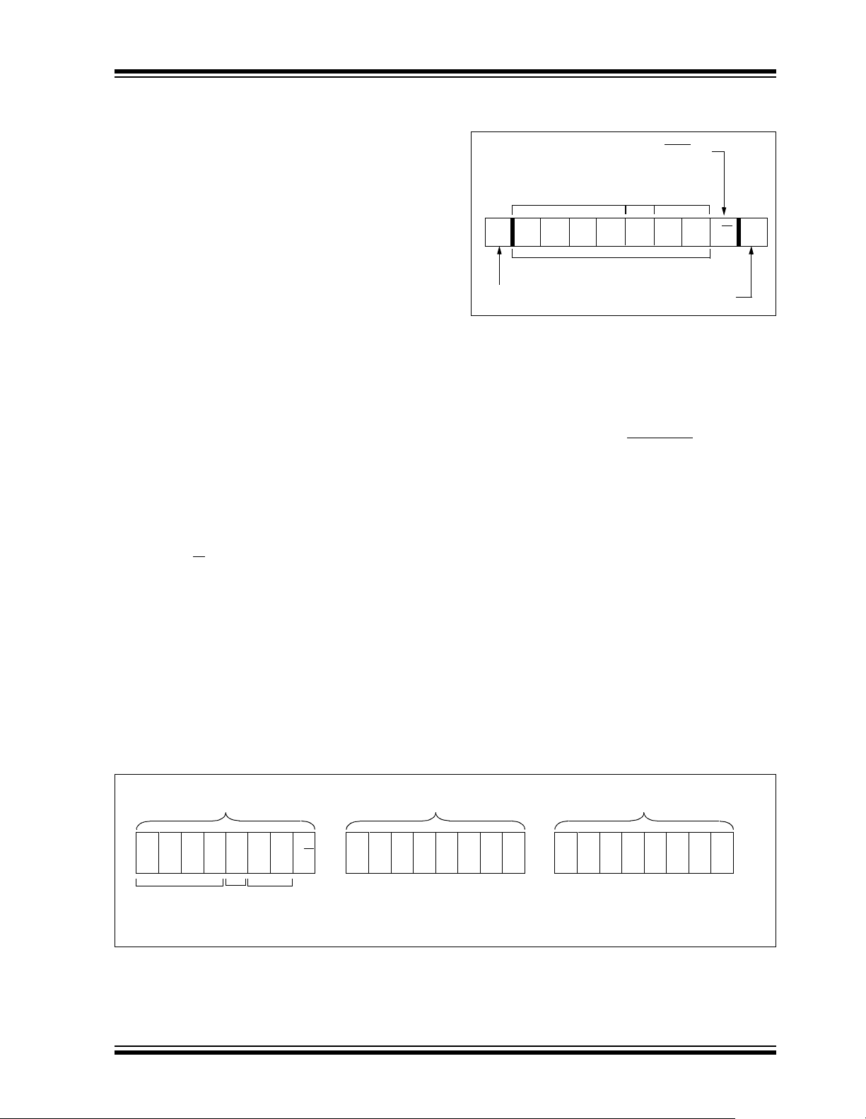
5.0 DEVICE ADDRESSING
A control byte is the first byte received following the
Start condition from the master device (Figure 5-1).
The control byte c onsis ts of a 4-bit c ontrol code; fo r the
24XX1025, this is set as ‘1010’ binary for read and
write operations. The next bit of the control byte is the
block select bit (B0). This bit acts as the A16 address
bit for accessing the entire array. The next two bits of
the control by te ar e the Chi p Select bits (A1, A0). T he
Chip Select bits allow the use of up to four 24XX1025
devices on the same bus and are used to select which
device is accessed. The Chip Select bits in the control
byte must correspond to the logic levels on the corresponding A1 and A0 pins for the device to respond.
These bits are in effect the two Most Significant bits of
the word address.
The last bit of the control byte defines the operation to
be performed. When set to a one, a read operation is
selected, and when set to a zero, a write operation is
selected. The next two bytes received define the
address of the first data byte (Figure 5-2). The upper
address bits are transferred first, followed by the Less
Significant bits.
Following the Start condition, the 24XX1025 monitors
the SDA bus checking the device type identifier being
transmitted. Upon receiving a ‘1010’ code and appropriate device select bits, the slave device outputs an
Acknowledge signal on the SDA line. Depending on the
state of the R /W
write operation.
This device has an internal addressing boundary
limitation that is divided into tw o segment s of 512K bits.
Block select bit ‘B0’ to control ac cess to each s egment.
bit, the 24XX1025 wil l sel ec t a re ad or
FIGURE 5-1: CONTROL BYTE
FORMAT
Chip
Select
Bits
Bit
Read/Write
Block
Select
Control Code
1010B0 A1 A0SACKR/W
Slave Address
Start Bit
Bits
Acknowledge Bit
5.1 Contiguous Addressing Across
Multiple Devices
The Chip Select bits A1, A0 can be used to exp and th e
contiguous add ress sp ace for up to 4 Mbit by add ing up
to four 24XX1025’s on the same bus. In this case,
software ca n use A0 of th e c ontr ol by te
A16 and A1 as address bit A17. It is not possible to
sequentially read across device boundaries.
Each device has internal addressing boundary
limitations. This divides each part into two segments of
512K bits. The block select bit ‘B0’ controls access to
each “half”.
Sequential read operations are limited to 512K blocks.
To read through four devices on the same bus, eight
random Read commands must be given.
as address bit
FIGURE 5-2: ADDRESS SEQUENCE BIT ASSIGNMENTS
Control Byte Address High Byte Address Low Byte
A
A
A
1 010
Control
Code
© 2007 Microchip Technology Inc. Preliminary DS21941E-page 7
B0A1A
Block
Select
Bit
0
Chip
Select
Bits
R/W
15
A
14
13
12
A11A10A
A
9
8
A
••••••
7
X = “don’t care” bit
A
0

24AA1025/24LC1025/24FC1025
6.0 WRITE OPERATIONS
6.1 Byte Write
Following the Start condition from the master, the
control code (four bits), the block select (one bit), the
Chip Select (two bits), and the R/W bit (w hi ch is a l ogi c
low) are clocked ont o the bus by the master tran smitter .
This indica tes t o t he ad d res se d s l av e r ece i ve r t ha t the
address high byte will follow after it has generated an
Acknowledge bit during the ninth clock cycle. Therefore, the next byte transmitted by the master is the
high-order byte of the word address and will be written
into the Address Pointer of the 24XX1025. The next
byte is the Least Sign ificant Ad dress Byte. Afte r receiving another Acknowledge signal from the 24XX1025,
the master device wil l transmit the data w ord to be written into the addressed memory location. The
24XX1025 acknowledge s again and the master gen erates a Stop condit ion. This init iates the intern al write
cycle and during this time, the 24XX1025 will not generate Acknow le dge s ignal s as long as the co ntro l byt e
being polled matches the control byte that was used to
initiate the write (Figure 6-1). If an attempt is made to
write to the array with the WP pin held high, the device
will acknowledge the command, but no write cycle will
occur, no data will be written and the device will
immediately accep t a new comman d. After a byte W rite
command, the interna l addre ss co unter wil l point to th e
address location following the one that was just written.
6.3 Write Protection
The WP pin a llows t he user to wri te-prot ect the entire
array (00000-1FFFF) when the pi n is tied to V
SS the write protection is disabled. The WP pin is
to V
sampled at the Stop bit for every Write command
(Figure 1-1). Toggling the WP pin after the Stop bit will
have no effect on the execution of the write cycle.
Note: Page write operations are lim ited to writin g
bytes within a single physical page,
regardless of the number o f by tes ac tua ll y
being written. Physical page boundaries
start at addresses that are integer
multiples of the page buffer size (or ‘page
size’) and end at addresses that are
integer multiples of [page size – 1]. If a
Page Write command attempts to write
across a physical page boundary, the
result is that the data wraps around to the
beginning of the current page (overwriting
data previously stored there), instead of
being written to the next p age as might be
expected. It is therefore, nece ssary for the
application software to prevent page write
operations that would attempt to cross a
page boundary.
CC. If tied
6.2 Page Write
The write control byte, word address and the first data
byte are transmitted to the 24XX1025 in the same way
as in a byte write. But instead of generating a Stop
condition, the master transmits up to 127 additional
bytes, which are temporarily stored in the on-ch ip page
buffer and will be wri tten int o memor y aft er th e maste r
has transmitted a Stop condition. After receipt of each
word, the seven lower Address Poin ter bits are internally incremented by one. If the mast er should trans mit
more than 128 bytes prior to generating the Stop condition, the address counter will roll over and the previously received data will be overwritte n. As with the byte
write operation, o nce the Stop condition is recei ved, a n
internal write cycl e will be gin (Fi gure6-2). If an att empt
is made to write to th e ar ray w ith t he W P pi n he ld hig h,
the device will acknow ledge the command , but no write
cycle will occur, no data will be written and the device
will immediately accept a new command.
DS21941E-page 8 Preliminary © 2007 Microchip Technology Inc.

FIGURE 6-1: BYTE WRITE
BUS ACTIVITY
MASTER
SDA LINE
BUS ACTIVITY
X = “don’t care” bit
S
T
Control
A
Byte
R
T
A1A
S 1010 0
B
0
0
FIGURE 6-2: PAGE WRITE
S
T
BUS ACTIVITY
MASTER
SDA LINE
BUS ACTIVITY
X = “don’t care” bit
Control
A
R
T
S 10 10 0
Byte
B0A1A
0
24AA1025/24LC1025/24FC1025
S
T
O
P
A
C
K
A
C
K
P
Data Byte 127
S
T
O
P
P
A
C
K
A
C
K
A
C
K
Address
High Byte
Address
High Byte
A
C
K
A
C
K
Address
Low Byte
Address
Low Byte
Data
A
C
K
Data Byte 0
A
C
K
© 2007 Microchip Technology Inc. Preliminary DS21941E-page 9

24AA1025/24LC1025/24FC1025
7.0 ACKNOWLEDGE POLLING
Since the device will not acknowledge during a write
cycle, this can be used to determine when the cycle is
complete. (This feature can be used to maximize bus
throughput.) Once the Stop condition for a Write
command has been issu ed from the mas ter , the device
initiates the internally timed write cycle. ACK polling
can be initiated immediately. This involves the master
sending a Start condition, followed by the control byte
for a Write command (R/W
busy with the write cycle, then no ACK will be returned.
If no ACK is returne d, then th e S t art bit and control byte
must be resent. I f the cyc le is compl ete, then th e device
will return the ACK and the master can then proceed
with the next Read or Write command. See Figure 7-1
for flow diagram.
Note: Care must be taken when polling the
24XX1025. The co ntrol byte that was use d
to initiate the write needs to match the
control byte used for polling.
= 0). If the device is still
FIGURE 7-1: ACKNOWLEDGE
POLLING FLOW
Send
Write Command
Send Stop
Condition to
Initiate Write Cycle
Send Start
Send Control Byte
with R/W = 0
Did Device
Acknowledge
(ACK = 0)?
No
Yes
Next
Operation
DS21941E-page 10 Preliminary © 2007 Microchip Technology Inc.

24AA1025/24LC1025/24FC1025
8.0 READ OPERATION
Read operations are initiated in the same way as write
operations with the exception that the R/W
control byte is set to one. There are three basic types
of read operation s: current address re ad, rando m read,
and sequential read.
8.1 Current Address Read
The 24XX1025 cont ains an ad dress co unter th at mai ntains the address of the last word accessed, internally
incremented by one. Therefore, if the previous read
access was to address n (n is any legal address), the
next current address read operati on would access da ta
from address n + 1.
Upon receipt of the c ontrol byte with R/W
the 24XX1025 issues an acknowledge and transmits
the 8-bit data word. The master will not acknowledge
the transfer , but does generate a S top con dition and the
24XX1025 discontinues trans mis sio n (Figu re8-1).
FIGURE 8-1: CURRENT ADDRESS
READ
S
BUS ACTIVITY
MASTER
SDA LINE
BUS ACTIVITY
T
A
R
T
1100
Control
Byte
BAA
010
1
A
C
K
bit of the
bit set to one,
Data
Byte
N
O
A
C
K
S
T
O
P
PS
8.2 Random Read
Random read operations allow the master to access
any memory location in a random manner. To perform
this type of read operat io n, fi rst the w o rd ad dres s m ust
be set. This is d one by sending the word a ddress to th e
24XX1025 as part of a write operation (R/W
bit set to
0). After the word address is sent, the master gener-
ates a Start condition following the acknowledge. This
terminates the write o pera tio n, b ut n ot be fore the internal Address Pointer is set. Then, the master issues the
control byte again, but with the R/W
bit set to a one.
The 24XX1025 will then issue an acknowledge and
transmit the 8-bit data word. The master will not
acknowledge the transfer, but does generate a Stop
condition which causes the 24XX1025 to discontinue
transmission (Figure 8-2). After a random Read
command, the interna l address counte r will po int to th e
address location following the one that was just read.
8.3 Sequential Read
Sequential reads are initiated in the same way as a
random read except that after the 24XX1025 transmits
the first data byte, the master issues an acknowledge
as opposed to the Stop condition used in a random
read. This acknowledge directs the 24XX1025 to trans mit the next sequentially addressed 8-bit word
(Figure 8-3). Following the final byte transmitted to the
master , the m aster w ill NOT generate an ackn owledg e,
but will generate a Stop condition. To provide sequential reads, the 24XX1025 contains an internal Address
Pointer which is incremented by one at the completion
of each operation. This Add ress Poin ter allows half the
memory contents to be serially read during one operation. Sequential rea d a ddre ss boundaries are 0000h to
FFFFh and 10000h to 1FFFFh. The internal Address
Pointer will automatically roll over from address FFFF
to address 0000 if the master acknowledges the byte
received from the array address, 1FFFF. The internal
address counter will automatically roll over from
address 1FFFFh to address 10000h if the master
acknowledges the byte received from the array
address, 1FFFFh.
© 2007 Microchip Technology Inc. Preliminary DS21941E-page 11

24AA1025/24LC1025/24FC1025
FIGURE 8-2: RANDOM READ
BUS ACTIVITY
MASTER
SDA LINE
BUS ACTIVITY
S
T
Control
A
R
T
S 1010
Byte
BAA
010
Address
High Byte
0
A
C
K
FIGURE 8-3: SEQUENTIAL READ
Address
Low Byte
A
C
K
S
T
A
R
T
S1010
A
C
K
Control
Byte
BAA
010
Data
Byte
1
A
C
K
S
T
O
P
P
N
O
A
C
K
BUS ACTIVITY
MASTER
SDA LINE
BUS ACTIVITY
Control
Byte
Data n Data n + 1
A
C
K
S
Data n + 2
A
C
K
A
C
K
A
C
K
Data n + X
T
O
P
P
N
O
A
C
K
DS21941E-page 12 Preliminary © 2007 Microchip Technology Inc.
24AA1025/24LC1025/24FC1025
9.0 PACKAGING INFORMATION
9.1 Package Marking Information
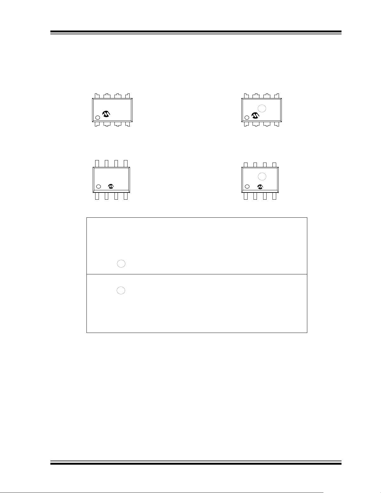
8-Lead PDIP (300 mil)
XXXXXXXX
TXXXXNNN
YYWW
8-Lead SOIJ (5.28 mm)
XXXXXXXX
TXXXXXXX
YYWWNNN
Legend: XX...X Part number or part number code
T Temperature (I, E)
Y Year code (last digit of calendar year)
YY Year code (last 2 digits of calendar year)
WW Week code (week of January 1 is week ‘01’)
NNN Alphanumeric traceability code (2 characters for small packages)
3
e
Pb-free JEDEC designator for Matte Tin (Sn)
Example:
24LC1025
I/P 13F
e
Example
24LC1025
e
I/SM
0510 13F
3
0601
:
3
Note: For very small packages with no room for the Pb-free JEDEC designator
, the marking will only appear on the outer carton or reel label.
3
e
Note: In the event the full Microch ip p art numb er canno t be mark ed on one l ine, it will
be carried over to the next line, thus limiting the number of available
characters for customer-specific information.
* Standard marking consists of Microchip part number, year code, week code, traceability code (facility
code, mask rev#, and assembly code). For marking beyond this, certain price adders apply. Please
check with your Microchip Sales Office.
© 2007 Microchip Technology Inc. Preliminary DS21941E-page 13

24AA1025/24LC1025/24FC1025
8-Lead Plastic Dual In-Line (P or PA) – 300 mil Body [PDIP]
N
1
2
3
4
Note: For the most current package drawings, please see the Microchip Packaging Specification located at
http://www.microchip.com/packaging
N
Units INCHES
Dimension Limits MIN NOM MAX
Number of Pins N 8
Pitch e .100 BSC
Top to Seating Plane A – – .210
Molded Package Thickness A2 .115 .130 .195
Base to Seating Plane A1 .015 – –
Shoulder to Shoulder Width E .290 .310 .325
Molded Package Width E1 .240 .250 .280
Overall Length D .348 .365 .400
Tip to Seating Plane L .115 .130 .150
Lead Thickness c .008 .010 .015
Upper Lead Width b1 .040 .060 .070
Lower Lead Width b .014 .018 .022
Overall Row Spacing § eB – – .430
otes:
. Pin 1 visual index feature may vary, but must be located with the hatched area.
. § Significant Characteristic.
. Dimensions D and E1 do not include mold flash or protrusions. Mold flash or protrusions shall not exceed .010" per side.
. Dimensioning and tolerancing per ASME Y14.5M.
BSC: Basic Dimension. Theoretically exact value shown without tolerances.
DS21941E-page 14 Preliminary © 2007 Microchip Technology Inc.

24AA1025/24LC1025/24FC1025
8-Lead Plastic Small Outline (SM) – Medium, 5.28 mm Body [SOIJ]
N
1
2
3
B
Note: For the most current package drawings, please see the Microchip Packaging Specification located at
http://www.microchip.com/packaging
D
N
E
E1
12
b
A
A1
Number of Pins N 8
Pitch e 1.27 BSC
Overall Height A 1.77 – 2.03
Molded Package Thickness A2 1.75 – 1.98
Standoff § A1 0.05 – 0.25
Overall Width E 7.62 – 8.26
Molded Package Width E1 5.11 – 5.38
Overall Length D 5.13 – 5.33
Foot Length L 0.51 – 0.76
Foot Angle φ 0° – 8°
Lead Thickness c 0.15 – 0.25
Lead Width b 0.36 – 0.51
Mold Draft Angle Top α – – 15°
Mold Draft Angle Bottom β – – 15°
otes:
. SOIJ, JEITA/EIAJ Standard, formerly called SOIC.
. § Significant Characteristic.
. Dimensions D and E1 do not include mold flash or protrusions. Mold flash or protrusions shall not exceed 0.25 mm per side.
e
α
A2
c
β
Units MILLIMETERS
Dimension Limits MIN NOM MAX
Microchip Technology Drawing C04-056
φ
L
© 2007 Microchip Technology Inc. Preliminary DS21941E-page 15

24AA1025/24LC1025/24FC1025
APPENDIX A: REVISION HISTORY
Revision A
Original release.
Revision B
Section 1.0 Electrical Characteristics: revised Ambient
Temperature; Revised Table 1-1; Revised Section 2.1
and Section 2.5.
Revision C
Revised Features, Maximum Read Current and Table
1-1, D9; Revised Table 2-1, V
Revision D (01/2007)
Revised Device Selection Table; Features Section;
Changed 1.8V to 1.7V; Revised Tables 1-1, 1-2, 2-1;
Revised Product ID System; Replaced Package
Drawings.
CC; Revised Section 6.3.
Revision E (03/2007)
Replaced Package Drawings (Rev. AM).
DS21941E-page 16 Preliminary © 2007 Microchip Technology Inc.

24AA1025/24LC1025/24FC1025
THE MICROCHIP WEB SITE
Microchip provides onlin e support v ia our W WW site at
www.m ic roc hi p.c om . Thi s web si te i s us ed as a m ean s
to make files and information easily available to
customers. Accessible by using your favorite Internet
browser, the web site contains the following
information:
• Product Support – Data sheets and errata,
application notes and sample programs, design
resources, user’s guides and hardware support
documents, lat est softwa re releases and archived
software
• General Technical Support – Frequently Asked
Questions (FAQ), technical support requests,
online discussion groups, Microchip consultan t
program member listing
• Business of Microchip – Product selector and
ordering guides, latest Microchip press releases,
listing of s eminars and events, listings of
Microchip sales offices, distributors and factory
representatives
CUSTOMER CHANGE NOTIFICATION SERVICE
CUSTOMER SUPPORT
Users of Microchip products can receive assistance
through several channels:
• Distributor or Representative
• Local Sales Office
• Field Application Engineer (FAE)
• Technical Support
• Development Systems Information Line
Customers should contact their distributor,
representative or field application engineer (FAE) for
support. Local sales offices are also available to help
customers. A listing of sales offices and locations is
included in the back of this document.
T echnic al support is avail able throug h the web si te
at: http://support.microchip.com
Microchip’s customer notification service helps keep
customers current on Microchip products. Subscribers
will receive e-mail notification whenever there are
changes, updates, revisions or errata related to a
specified produ ct family or develo pment tool of inte rest.
To register, access the Microchip web site at
www.microchip.com, click on Customer Change
Notification and follow the registration instructions.
© 2007 Microchip Technology Inc. Preliminary DS21941E-page 17

24AA1025/24LC1025/24FC1025
READER RESPONSE
It is our intentio n to pro vi de you with the best documentation possible to ens ure suc c es sfu l u se of y ou r M ic roc hip product. If you wish to provid e your c omment s on org anizatio n, clarity, subject matter, and ways in w hich o ur docum entatio n
can better serve you, please FAX your comments to the Technical Publications Manager at (480) 792-4150.
Please list the following information, and use this outline to provide us with your comments about this document.
To:
RE: Reader Response
From:
Application (optional):
Would you like a reply? Y N
Device: Literature Number:
Questions:
1. What are the best features of this document?
2. How does this document meet your hardware and software development needs?
3. Do you find the organization of this document easy to follow? If not, why?
Technical Publications Manager
Name
Company
Address
City / State / ZIP / Country
Telephone: (_______) _________ - _________
Total Pages Sent ________
FAX: (______) _________ - _________
DS21941E24AA1025/24LC1025/24FC1025
4. What additions to the document do you think would enhance the structure and subject?
5. What deletions from the document could be made without affecting the overall usefulness?
6. Is there any incorrect or misleading information (what and where)?
7. How would you improve this document?
DS21941E-page 18 Preliminary © 2007 Microchip Technology Inc.

24AA1025/24LC1025/24FC1025
PRODUCT IDENTIFICATION SYSTEM
To order or obtain information, e.g., on pricing or delivery, refer to the factory or the listed sales office.
PART NO. X /XX
Device
PackageTemperature
Range
Device: 24AA1025: = 1024K Bit 1.7V I2C CMOS Serial EEPROM
24AA1025T:= 1024K Bit 1.7V I
24LC1025: = 1024K Bit 2.5V I
24LC1025T:= 1024K Bit 2.5V I
24FC1025: = 1024K Bit 2.5V I
24FC1025T:= 1024K Bit 2.5V I
(Tape and Reel)
(Tape and Reel)
(Tape and Reel)
2
C CMOS Serial EEPROM
2
C CMOS Serial EEPROM
2
C CMOS Serial EEPROM
2
C CMOS Serial EEPROM
2
C CMOS Serial EEPROM
Examples:
a) 24AA1025T-I/SM: Tape and Reel, Indus trial
Temperature, SOIJ package.
b) 24LC1025-I/P: Industrial Temperature,
PDIP package.
c) 24LC1025-E/SM: Extended Temperature,
SOIJ package.
d) 24LC1025T-I/SM: Tape and Reel, Industrial
Temperature, SOIJ package.
Temperature
Range:
Package: P = Plastic DIP (300 mil Body), 8-lead
I = -40°C to +85°C
E = -40°C to +125°C
SM = Plastic SOIJ (5.28 mm Body), 8-lead
© 2007 Microchip Technology Inc. Preliminary DS21941E-page 19

24AA1025/24LC1025/24FC1025
NOTES:
DS21941E-page 20 Preliminary © 2007 Microchip Technology Inc.

Note the following details of the code protection feature on Microchip devices:
• Microchip products meet the specification contained in their particular Microchip Data Sheet.
• Microchip believes that its family of products is one of the most secure families of its kind on the market today, when used in the
intended manner and under normal conditions.
• There are dishonest and possibly illegal methods used to breach the code protection feature. All of these methods, to our
knowledge, require using the Microchip products in a manner outside the operating specifications contained in Microchip’s Data
Sheets. Most likely, the person doing so is engaged in theft of intellectual property.
• Microchip is willing to work with the customer who is concerned about the integrity of their code.
• Neither Microchip nor any other semiconductor manufacturer can guarantee the security of their code. Code protection does not
mean that we are guaranteeing the product as “unbreakable.”
Code protection is constantly evolving. We at Microchip are com mitted to continuously improving the code protect ion f eatures of our
products. Attempts to break Microchip’s code protection feature may be a violation of the Digit al Mill ennium Copyright Act. If such acts
allow unauthorized access to your software or other copyrighted work, you may have a right to sue for relief under that Act.
Information contained in this publication regarding device
applications and t he lik e is provided only for your convenience
and may be su perseded by upda t es . I t is y o u r r es ponsibility to
ensure that your application meets with your specifications.
MICROCHIP MAKES NO REPRESENTATIONS OR
WARRANTIES OF ANY KIND WHETHER EXPRESS OR
IMPLIED, WRITTEN OR ORAL, STATUTORY OR
OTHERWISE, RELATED TO THE INFORMATION,
INCLUDING BUT NOT LIMITED TO ITS CONDITION,
QUALITY, PERFORMANCE, MERCHANTABILITY OR
FITNESS FOR PURPOSE. Microchip disclaims all liability
arising from this information and its use. Use of Microchip
devices in life supp ort and/or safety ap plications is entir ely at
the buyer’s risk, and the buyer agrees to defend, indemnify and
hold harmless M icrochip from any and all dama ges, claims,
suits, or expenses re sulting from such use. No licens es are
conveyed, implicitly or otherwise, under any Microchip
intellectual property rights.
Trademarks
The Microchip name and logo, the Microchip logo, Accuron,
dsPIC, K
EELOQ, KEELOQ logo, microID, MPLAB, PIC,
PICmicro, PICSTART, PRO MATE, PowerSmart, rfPIC, and
SmartShunt are registered trademarks of Microchip
Technology Incorporated in the U.S.A. and other countries.
AmpLab, FilterLab, Linear Active Thermistor, Migratable
Memory, MXDEV, MXLAB, PS logo, SEEVAL, SmartSensor
and The Embedded Control Solutions Company are
registered trademarks of Microchip Technology Incorporated
in the U.S.A.
Analog-for-the-Digital Age, Application Maestro, CodeGuard,
dsPICDEM, dsPICDEM.net, dsPICworks, ECAN,
ECONOMONITOR, FanSense, FlexROM, fuzzyLAB,
In-Circuit Serial Programming, ICSP, ICEPIC, Mindi, MiWi,
MPASM, MPLAB Certified logo, MPLIB, MPLINK, PICkit,
PICDEM, PICDEM.net, PICLAB, PICtail, PowerCal,
PowerInfo, PowerMate, Pow e rTool, REAL ICE, rfLAB,
rfPICDEM, Select Mode, Smart Serial, SmartTel, Total
Endurance, UNI/O, WiperLock and ZENA are trademarks of
Microchip Technology Incorporated in the U.S.A. and other
countries.
SQTP is a service mark of Microchip T echnology Incorporated
in the U.S.A.
All other trademarks mentioned herein are property of their
respective companies.
© 2007, Microchip Technology Incorporated, Printed in the
U.S.A., All Rights Reserved.
Printed on recycled paper.
Microchip received ISO/TS-16949:2002 certification for its worldwide
headquarters, design and wafer fabrication facilities in Chandler and
Tempe, Arizona, Gresham, Oregon and Mountain View, California. The
Company’s quality system processes and procedures are for its PIC
MCUs and dsPIC® DSCs, KEELOQ
EEPROMs, microperipherals, nonvolatile memory and analog
products. In addition, Microchip’s quality system for the design and
manufacture of development systems is ISO 9001:2000 certified.
®
code hopping devices, Serial
© 2007 Microchip Technology Inc. Preliminary DS21941E-page 21
®

WORLDWIDE SALES AND SERVICE
AMERICAS
Corporate Office
2355 West Chandler Blvd.
Chandler, AZ 85224-6199
Tel: 480-792-7200
Fax: 480-792-7277
Technical Support:
http://support.microchip.com
Web Address:
www.microchip.com
Atlanta
Duluth, GA
Tel: 678-957-9614
Fax: 678-957-1455
Boston
Westborough, MA
Tel: 774-760-0087
Fax: 774-760-0088
Chicago
Itasca, IL
Tel: 630-285-0071
Fax: 630-285-0075
Dallas
Addison, TX
Tel: 972-818-7423
Fax: 972-818-2924
Detroit
Farmington Hills, MI
Tel: 248-538-2250
Fax: 248-538-2260
Kokomo
Kokomo, IN
Tel: 765-864-8360
Fax: 765-864-8387
Los Angeles
Mission Viejo, CA
Tel: 949-462-9523
Fax: 949-462-9608
Santa Clara
Santa Clara, CA
Tel: 408-961-6444
Fax: 408-961-6445
Toronto
Mississauga, Ontario,
Canada
Tel: 905-673-0699
Fax: 905-673-6509
ASIA/PACIFIC
Asia Pacific Office
Suites 3707-14, 37th Floor
Tower 6, The Gateway
Habour City, Kowloon
Hong Kong
Tel: 852-2401-1200
Fax: 852-2401-3431
Australia - Sydney
Tel: 61-2-9868-6733
Fax: 61-2-9868-6755
China - Beijing
Tel: 86-10-8528-2100
Fax: 86-10-8528-2104
China - Chengdu
Tel: 86-28-8665-5511
Fax: 86-28-8665-7889
China - Fuzhou
Tel: 86-591-8750-3506
Fax: 86-591-8750-3521
China - Hong Kong SAR
Tel: 852-2401-1200
Fax: 852-2401-3431
China - Qingdao
Tel: 86-532-8502-7355
Fax: 86-532-8502-7205
China - Shanghai
Tel: 86-21-5407-5533
Fax: 86-21-5407-5066
China - Shenyang
Tel: 86-24-2334-2829
Fax: 86-24-2334-2393
China - Shenzhen
Tel: 86-755-8203-2660
Fax: 86-755-8203-1760
China - Shunde
Tel: 86-757-2839-5507
Fax: 86-757-2839-5571
China - Wuhan
Tel: 86-27-5980-5300
Fax: 86-27-5980-5118
China - Xian
Tel: 86-29-8833-7250
Fax: 86-29-8833-7256
ASIA/PACIFIC
India - Bangalore
Tel: 91-80-4182-8400
Fax: 91-80-4182-8422
India - New Delhi
Tel: 91-11-4160-8631
Fax: 91-11-4160-8632
India - Pune
Tel: 91-20-2566-1512
Fax: 91-20-2566-1513
Japan - Yokohama
Tel: 81-45-471- 6166
Fax: 81-45-471-6122
Korea - Gumi
Tel: 82-54-473-4301
Fax: 82-54-473-4302
Korea - Seoul
Tel: 82-2-554-7200
Fax: 82-2-558-5932 or
82-2-558-5934
Malaysia - Penang
Tel: 60-4-646-8870
Fax: 60-4-646-5086
Philippines - Manila
Tel: 63-2-634-9065
Fax: 63-2-634-9069
Singapore
Tel: 65-6334-8870
Fax: 65-6334-8850
Taiwan - Hsin Chu
Tel: 886-3-572-9526
Fax: 886-3-572-6459
Taiwan - Kaohsiung
Tel: 886-7-536-4818
Fax: 886-7-536-4803
Taiwan - Taipei
Tel: 886-2-2500-6610
Fax: 886-2-2508-0102
Thailand - Bangkok
Tel: 66-2-694-1351
Fax: 66-2-694-1350
EUROPE
Austria - Wels
Tel: 43-7242-2244-39
Fax: 43-7242-2244-393
Denmark - Copenhagen
Tel: 45-4450-2828
Fax: 45-4485-2829
France - Paris
Tel: 33-1-69-53-63-20
Fax: 33-1-69-30-90-79
Germany - Munich
Tel: 49-89-627-144-0
Fax: 49-89-627-144-44
Italy - Milan
Tel: 39-0331-742611
Fax: 39-0331-466781
Netherlands - Drunen
Tel: 31-416-690399
Fax: 31-416-690340
Spain - Madrid
Tel: 34-91-708-08-90
Fax: 34-91-708-08-91
UK - Wokingham
Tel: 44-118-921-5869
Fax: 44-118-921-5820
12/08/06
DS21941E-page 22 Preliminary © 2007 Microchip Technology Inc.
 Loading...