

Page 1
24AA256/24LC256/24FC256
256K I2C™ CMOS Serial EEPROM
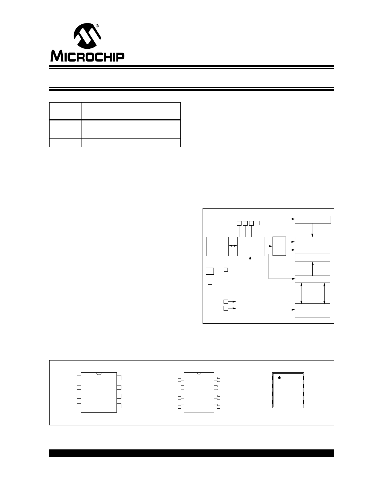
Device Selection Table
Part
Number
VCC
Range
Max. Clock
Frequency
24AA256 1.8-5.5V 400 kHz
24LC256 2.5-5.5V 400 kHz I, E
24FC256 1.8-5.5V 1 MHz
(2)
Note 1: 100 kHz for VCC < 2.5V.
2: 400 kHz for VCC < 2.5V.
(1)
Temp.
Ranges
I
I
Features:
• Low-power CMOS technology:
- Maximum write current 3mA at 5.5V
- Maximum read current 400 μA at 5.5V
- Standby curren t 100 nA, typical at 5.5V
• 2-wire serial interface bus, I
• Cascadable for up to eight devices
• Self-timed erase/write cycle
• 64-byte Page Write mode available
• 5 ms max. write cycle time
• Hardware write-protect for entire array
• Output slope control to eliminate ground bounce
• Schmitt Trigger inputs for nois e suppression
• 1,000,000 erase/write cycles
• Electrostatic discharge protection > 4000V
• Data retention > 200 years
• 8-pin PDIP, SOIC, TSSOP, MSOP and DFN
packages, 14-lead TSSOP package
• Pb-free finishes available
• Temperature ranges:
- Industrial (I): -40°C to +85°C
- Automotive (E): -40°C to +125°C
2C™
compatible
Description:
The Microchip Technology Inc. 24AA256/24LC256/
24FC256 (24XX256*) is a 32K x 8 (256 Kbit) Serial
Electrically Erasable PROM, capable of operation
across a broad voltage range (1.8V to 5.5V). It has
been developed for advanced, low-power applications
such as personal communications or data acquisition.
This device al so has a page write capability of up to 64
bytes of data. This device is capable of both random
and sequential reads up to the 256K boundary.
Functional address lines allow up to eight devices on
the same bus, for up to 2 Mbit address space. This
device is available in the standard 8-pin plastic DIP,
SOIC, TSSOP, MSOP and DFN packages.
Block Diagram
A0 A1A2
I/O
SDA
I/O
Control
Logic
V
CC
VSS
SCL
Memory
Control
Logic
WP
XDEC
HV Generator
EEPROM
Array
Page Latches
YDEC
Sense Amp.
R/W Control
Package Types
PDIP/SOIC TSSOP/MSOP*
1
A0
2
A1
3
A2
SS
4
V
Note: * Pins A0 and A1 are no connects for the MSOP package only.
8
VCC
WP
7
SCL
6
24XX256
SDA
5
1
A0
2
A1
3
A2
4
V
SS
24XX256
8
CC
V
7
WP
6
SCL
5
SDA
A0
A1
A2
SS
V
*24XX256 is used in this document as a generic part number for the 24AA256/24LC256/24FC256 devices.
© 2005 Microchip Technology Inc. DS21203N-page 1
DFN
1
2
3
4
8
VCC
7
WP
6
SCL
24XX256
5
SDA
Page 2
24AA256/24LC256/24FC256
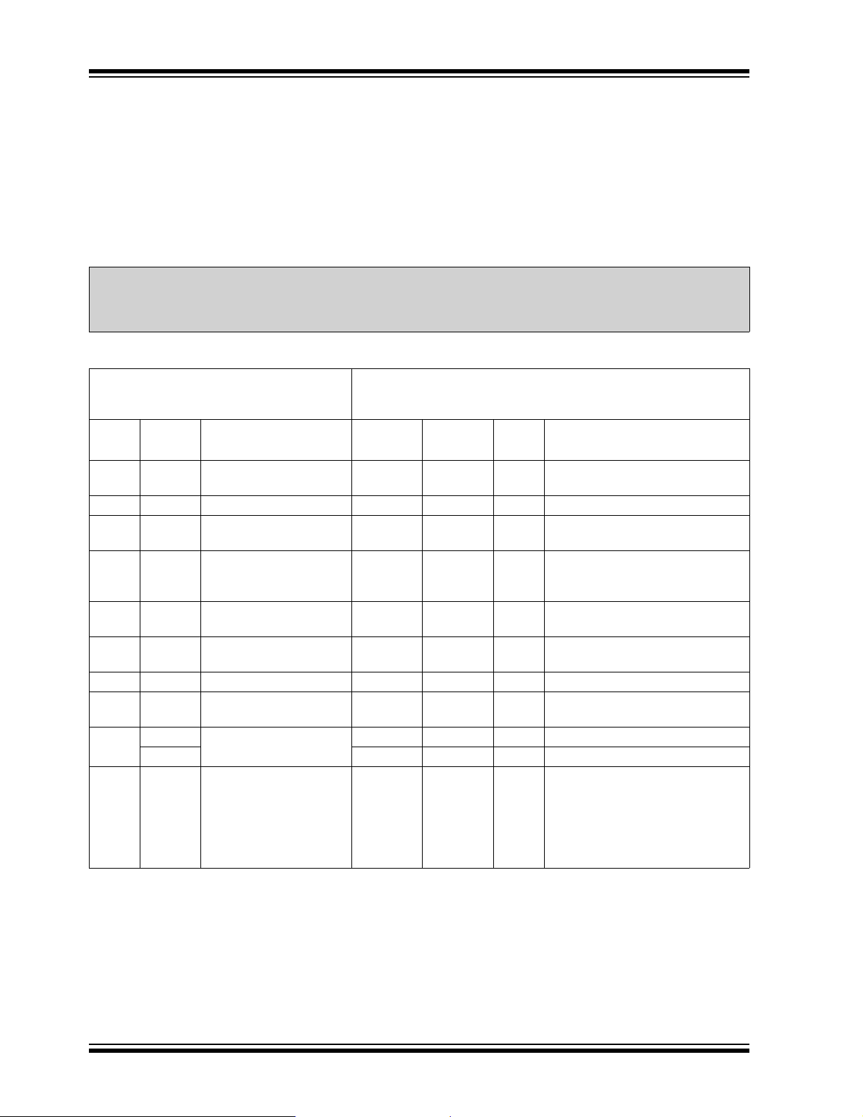
1.0 ELECTR ICAL CHARACTERISTICS
Absolute Maximum Ratings
(†)
VCC.............................................................................................................................................................................6.5V
All inputs and outputs w.r.t. V
SS ......................................................................................................... -0.6V to VCC +1.0V
Storage temperature ...............................................................................................................................-65°C to +150°C
Ambient temperature with power applied................................................................................................-40°C to +125°C
ESD protection on all pins ......................................................................................................................................................≥ 4kV
† NOTICE: Stresses above those listed under “Absolute Maximum Ratings” may cause permanent damage to the
device. This is a stres s ratin g only and func tional operati on of the devic e at thes e or any other co nditio ns abov e thos e
indicated in the operational listings of this specification is not implied. Exposure to Absolute Maximum Rating
conditions for extended periods may affect device reliability.
TABLE 1-1: DC CHARACTERISTICS
Electrical Characteristics:
DC CHARACTERISTICS
Param.
No.
Sym. Characteristic Min. Max. Units Conditions
D1 — A0, A1, A2, SCL, SDA
and WP pins:
D2 V
D3 V
IH High-level input voltage 0.7 VCC —V—
IL Low-level input voltage — 0.3 VCC
D4 VHYS Hysteresis of Schmitt
Trigger inputs
(SDA, SCL pins)
D5 VOL Low-level output voltage — 0.40 V IOL = 3.0 ma @ VCC = 4.5V
D6 ILI Input leakage current — ±1 μAVIN = VSS or VCC, WP = VSS
D7 ILO Output leakage current — ±1 μAVOUT = VSS or VCC
D8 CIN,
OUT
C
D9 I
CC Read Operating current — 400 μAVCC = 5.5V, SCL = 400 kHz
Pin capacitance
(all inputs/outpu t s)
ICC Write — 3 mA VCC = 5.5V
D10 ICCS Standby current — 1 μATA = -40°C to +85°C
Note: This parameter is periodically sampled and not 100% tested.
Industrial (I): VCC = +1.8V to 5.5V TA = -40°C to +85°C
Automotive (E): V
CC = +2.5V to 5.5V TA = -40°C to +125°C
————
VVVCC ≥ 2.5V
0.2 VCC
CC < 2.5V
V
0.05 VCC —VVCC ≥ 2.5V (Note)
I
OL = 2.1 ma @ VCC = 2.5V
VIN = VSS or VCC, WP = VCC
—10pFVCC = 5.0V (Note)
A = 25°C, FCLK = 1 MHz
T
SCL = SDA = V
A0, A1, A2, WP = V
CC = 5.5V
SS
—5μATA = -40°C to +125°C
SCL = SDA = V
A0, A1, A2, WP = V
CC = 5.5V
SS
DS21203N-page 2 © 2005 Microchip Technology Inc.
Page 3

24AA256/24LC256/24FC256
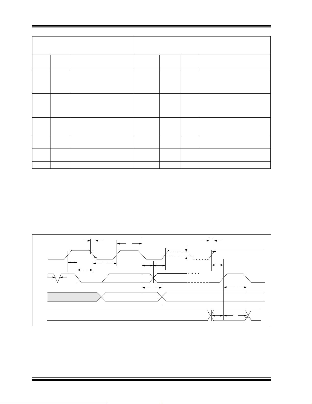
TABLE 1-2: AC CHARACTERISTICS
Electrical Characteristics:
AC CHARACTERISTICS
Param.
No.
1F
Sym. Characteristic Min. Max. Units Conditions
CLK Clock frequency —
2THIGH Clock high time 4000
3T
LOW Clock low time 4700
4TR SDA and SCL rise time
(Note 1)
5TF SDA and SCL fall time
(Note 1)
6T
HD:STA Start condition hold time 4000
7TSU:STA Start condition setup time 4700
8THD:DAT Data input hold time 0 — ns (Note 2)
9T
10 T
SU:DAT Data input setup time 250
SU:STO Stop condition setup time 4000
11 TSU:WP WP setup time 4000
12 THD:WP WP hold time 4700
Note 1: Not 100% tested. CB = total capacitance of one bus line in pF.
2: As a transmitter, the device must provide an internal minimum delay time to bridge the undefined region
(minimum 300 ns) of the falling edge of SCL to avoid unintended generation of Start or Stop conditions.
3: The combined T
SP and VHYS specificati ons ar e due to n ew Schmitt T rigger inputs , which p rovide im proved
noise spike suppression. This eliminates the need for a T
4: This parameter is not tested bu t ensured by characterization. For endurance estimates in a specific
application, ple ase consu lt the Tot al Endu rance™ M odel, wh ich can be obt ained fro m Microchi p’s web sit e
at www.microchip.com.
Industrial (I): VCC = +1.8V to 5.5V TA = -40°C to +85°C
Automotive (E): V
—
—
—
600
600
500
1300
1300
500
—
—
—
—
—
600
600
250
600
600
250
100
100
600
600
250
600
600
1300
1300
CC = +2.5V to 5.5V TA = -40°C to +125°C
100
400
400
1000
—
—
—
—
—
—
—
—
1000
300
300
300
100
—
—
—
—
—
—
—
—
—
—
—
—
—
—
—
—
—
—
—
—
—
kHz 1.8V ≤ VCC < 2.5V
2.5V ≤ V
1.8V ≤ V
2.5V ≤ V
CC ≤ 5.5V
CC < 2.5V 24FC256
CC ≤ 5.5V 24FC256
ns 1.8V ≤ VCC < 2.5V
2.5V ≤ V
1.8V ≤ V
2.5V ≤ V
CC ≤ 5.5V
CC < 2.5V 24FC256
CC ≤ 5.5V 24FC256
ns 1.8V ≤ VCC < 2.5V
2.5V ≤ V
1.8V ≤ V
2.5V ≤ V
CC ≤ 5.5V
CC < 2.5V 24FC256
CC ≤ 5.5V 24FC256
ns 1.8V ≤ VCC < 2.5V
2.5V ≤ V
1.8V ≤ V
CC ≤ 5.5V
CC ≤ 5.5V 24FC256
ns All except, 24FC256
1.8V ≤ V
CC ≤ 5.5V 24FC256
ns 1.8V ≤ VCC < 2.5V
2.5V ≤ V
1.8V ≤ V
2.5V ≤ V
CC ≤ 5.5V
CC < 2.5V 24FC256
CC ≤ 5.5V 24FC256
ns 1.8V ≤ VCC < 2.5V
2.5V ≤ V
1.8V ≤ V
2.5V ≤ V
ns 1.8V ≤ V
2.5V ≤ V
1.8V ≤ V
CC ≤ 5.5V
CC < 2.5V 24FC256
CC ≤ 5.5V 24FC256
CC < 2.5V
CC ≤ 5.5V
CC ≤ 5.5V 24FC256
ns 1.8V ≤ VCC < 2.5V
2.5V ≤ V
1.8V ≤ V
2.5V ≤ V
CC ≤ 5.5V
CC < 2.5V 24FC256
CC ≤ 5.5V 24FC256
ns 1.8V ≤ VCC < 2.5V
2.5V ≤ V
1.8V ≤ V
CC ≤ 5.5V
CC ≤ 5.5V 24FC256
ns 1.8V ≤ VCC < 2.5V
2.5V ≤ V
1.8V ≤ V
I specification for standard operation.
CC ≤ 5.5V
CC ≤ 5.5V 24FC256
© 2005 Microchip Technology Inc. DS21203N-page 3
Page 4
24AA256/24LC256/24FC256
Electrical Characteristics:
AC CHARACTERISTICS (Continued)
Param.
No.
Sym. Characteristic Min. Max. Units Conditions
13 TAA Output valid from clock
(Note 2)
14 TBUF Bus free time: Time the bus
must be free before a new
transmission can start
15 T
OF Output fall time from VIH
minimum to VIL maximum
B ≤ 100 pF
C
16 T
SP Input filt er spi ke su ppre ssion
(SDA and SCL pins)
17 T
WC Write cycle time (byte or
page)
18 — Endurance 1,000,000 — cycles 25°C (Note 4)
Note 1: Not 100% tested. C
B = total capacitance of one bus line in pF.
2: As a transmitter, the device must provide an internal minimum delay time to bridge the undefined region
(minimum 300 ns) of the falling edge of SCL to avoid unintended generation of Start or Stop conditions.
3: The combined T
SP and VHYS specific ations ar e due to n ew Schmitt T rigger inputs , which p rovide improved
noise spike suppression. This eliminates the need for a T
4: This parameter i s not tested bu t ensured by characterization. For en durance estimates in a spec ific
application, ple ase consu lt the Tot al Endu rance™ M odel, wh ich can be obt ained fro m Microchi p’s web sit e
at www.microchip.com.
Industrial (I): V
Automotive (E): V
—
—
—
—
4700
1300
1300
500
10 + 0.1CB 250
CC = +1.8V to 5.5V TA = -40°C to +85°C
CC = +2.5V to 5.5V TA = -40°C to +125°C
3500
900
900
400
—
—
—
—
ns 1.8 V ≤ VCC < 2.5V
2.5 V ≤ V
1.8V ≤ V
2.5 V ≤ V
CC ≤ 5.5V
CC < 2.5V 24FC256
CC ≤ 5.5V 24FC256
ns 1.8V ≤ VCC < 2.5V
2.5V ≤ V
1.8V ≤ V
2.5V ≤ V
CC ≤ 5.5V
CC < 2.5V 24FC256
CC ≤ 5.5V 24FC256
ns All except, 24FC256 (Note 1)
250
— 50 ns All except, 24FC256 (Notes 1
and 3)
—5ms—
I specification for standard operation.
FIGURE 1-1: BUS TIMING DATA
5
SCL
SDA
IN
SDA
OUT
WP
16
7
6
3
2
89
13
(protected)
(unprotected)
D4
4
10
14
11
12
DS21203N-page 4 © 2005 Microchip Technology Inc.
Page 5

24AA256/24LC256/24FC256
2.0 PIN DESCRIPTIONS
The descriptions of the pins are listed in Table 2-1.
TABLE 2-1: PIN FUNCTION TABLE
Name
A0 1 1 1 — 1 User Configurable Chip Select
A1 2 2 2 — 2 User Configurable Chip Select
(NC) — — — 1, 2 — Not Connected
A2 3 3 3 3 3 User Configurable Chip Select
SS 44444Ground
V
SDA 5 5 5 5 5 Serial Data
SCL 6 6 6 6 6 Serial Clock
(NC) — — — — — Not Connected
WP 7 7 7 7 7 Write-Protect Input
CC 8 8 8 8 8 +1.8V to 5.5V (24AA256)
V
8-pin
PDIP
8-pin
SOIC
8-pin
TSSOP
8-pin
MSOP
8-pin
DFN
Function
+2.5V to 5 .5V (24LC256)
+1.8V to 5 .5V (24FC256)
2.1 A0, A1, A2 Chip Address Inputs
The A0, A1 and A2 inputs are used by the 24XX256 for
multiple device operations. The levels on these inputs
are compared with the corresponding bits in the slave
address. The chip is selected if the compare is true.
For the MSOP pac kage only, pins A0 and A 1 are not
connected.
Up to eight devices (two for the MSOP package) may
be connected to the same bus by using different Chip
Select bit combinations. These inputs must be
connected to either V
In most applications, the chip address inputs A0, A1
and A2 are hard-wired to logic ‘0’ or logic ‘1’. For
applications in which these pins are controlled by a
microcontroller or other pro grammabl e device, the chi p
address pins must be driven to logic ‘0’ or logic ‘1’
before normal device operation can proceed.
CC or VSS.
2.2 Serial Data (SDA)
This is a bidirectional pin used to transfer addresses
and data into and out of the device. It is an open drain
terminal. Therefore, the SDA bus requires a pull-up
resistor to V
400kHz and 1MHz).
For normal data transfer, SDA is allowed to change
only during SCL low. Changes during SCL high are
reserved for indicating the Start and Stop conditions.
CC (typical 10 kΩ for 100 kHz, 2 kΩ for
2.3 Serial Clock (SCL)
This input is used to synchronize the data transfer to
and from the device.
2.4 Write-Protect (WP)
This pin must be conne cted to eithe r VSS or VCC. If tied
SS, write operations are enabled. If tied to VCC,
to V
write operations are inhibited but read operations are
not affected.
3.0 FUNCT IONAL DESCRIPTION
The 24XX256 supports a bidirectional 2-wire bus and
data transmission protocol. A device that sends data
onto the bus is defined as a transmitter and a device
receiving data as a receiver. The bus must be
controlled by a master device which generates the
Serial Clock (SCL), controls the bus access, and
generates the Start and Stop conditions while the
24XX256 works as a sla ve. Both master and slave ca n
operate as a transmitter or receiver, but the master
device determines which mode is activated.
© 2005 Microchip Technology Inc. DS21203N-page 5
Page 6

24AA256/24LC256/24FC256
4.0 BUS CHARAC TERISTICS
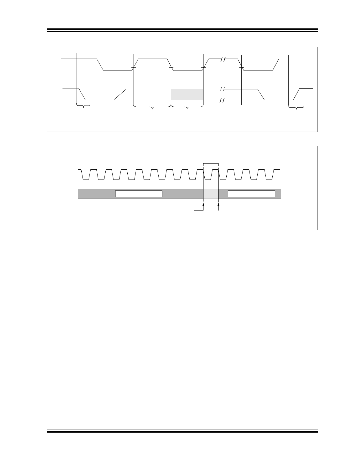
The following bus protocol has been defined:
• Data transfer may be initiated only when the bus
is not busy.
• During data transfer, the data line must remain
stable wheneve r the c lock lin e is high . Changes i n
the data line, while the clock line is high, will be
interpreted as a Start or Stop condition.
Accordingly, the following bus conditions have been
defined (Figure 4-1).
4.1 Bus Not Busy (A)
Both data and clock lines remain high.
4.2 Start Data Transfer (B)
A high-to-low transition of the SDA line while the clock
(SCL) is high, determines a Start condition. All
commands must be preceded by a Start condition.
4.3 Stop Data Transf er (C)
A low-to-high transition of the SDA li ne, while the cl ock
(SCL) is high, determines a Stop condition. All
operations must end with a Stop condition.
4.4 Data Valid (D)
The state of the data line represents valid data when,
after a Start condition, the data line is stable for the
duration of the high period of the clock signal.
The data on the line must be changed during the low
period of the clock signal. There is one bit of data per
clock pulse.
Each data transfer is initiated with a S tart condition and
terminated with a Stop condition. The number of the
data bytes transferred between the Start and Stop
conditions is determined by the master device.
4.5 Acknowledge
Each receiving device, when addressed, is obliged to
generate an Acknowledge signal after the reception of
each byte. The master device must generate an extra
clock pulse which is associated with this Acknowledge
bit.
Note: The 24XX256 does not generate any
Acknowledge bits if an internal
programming cycle is in progress.
A device that acknowledges must pull down the SDA
line during the acknowledge clock pulse in such a way
that the SDA line is sta ble low d uring the high pe riod of
the acknowledge related clock pulse. Of course, setup
and hold times must be taken into account. During
reads, a master m ust s ignal an end of dat a to the sl ave
by NOT generating an Acknow ledge bit on the las t byte
that has been cl ocke d out o f the slave . In th is ca se , the
slave (24XX256) will leave the data line high to enable
the master to generate the Stop condition.
DS21203N-page 6 © 2005 Microchip Technology Inc.
Page 7
24AA256/24LC256/24FC256
FIGURE 4-1: DATA TRANSFER SEQUENCE ON THE SERIAL BUS
(A) (B) (D) (D) (C) (A)
SCL
SDA
Start
Condition
Address or
Acknowledge
Valid
FIGURE 4-2: ACKNOWLEDGE TIMING
SCL
SDA
Transmitter must release the SDA line at this point,
allowing the Receiver to pull the SDA line low to
acknowledge the previous eight bits of data.
Data from transmitter
Data
Allowed
to Change
Stop
Condition
Acknowledge
Bit
987654321 123
Data from transmitter
Receiver must release the SDA line
at this point so the Transmitter can
continue sending data.
© 2005 Microchip Technology Inc. DS21203N-page 7
Page 8
24AA256/24LC256/24FC256
5.0 DEVICE ADDRESSING
A control byte is the first byte received following the
Start condition from the master device (Figure 5-1).
The control byte consi sts of a 4-bit contro l code. For the
24XX256, this is set as ‘
operations. The next three bits of the control byte are
the Chip Select bits (A2, A1, A0). The Chip Select bits
allow the use of up to eight 24XX256 devices on the
same bus and are used to select which device is
accessed. The Chip Select bits in the control byte must
correspond to the logic lev els on the corresp onding A2,
A1 and A0 pins for the device to respond. These bits
are, in effect, the thre e Most Signi ficant bit s of the word
address.
For the MSOP package, the A0 and A1 pins are not
connected. During device addressing, the A0 and A1
Chip Select bits (Figures 5-1 and 5-2) should be set to
‘0’. Only two 24XX256 MSOP packages can be
connected to the same bus.
The last bit of the control byte defines the operation to
be performed. When set to a one, a read operation is
selected. When set to a zero, a write operation is
selected. The next two bytes received define the
address of the first data byte (Figure 5-2). Because
only A14…A0 are used, the upper address bits are a
“don’t care.” The upper address bits are transferred
first, followed by the Less Significant bits.
Following the Start condition, the 24XX256 monitors
the SDA bus checking the device type identifier being
transmitted. Upon receiving a ‘
priate device select bits, the slave device outputs an
Acknowledge signal on the SDA line. Depending on the
state of the R/W
write operation.
1010’ binary for read and write
1010’ code and appro-
bit, the 24XX256 will select a read or
FIGURE 5-1: CONTROL BYTE
FORMAT
Bit
Bits
ACKR/W
Acknowledge Bit
S
Start Bi t
Control Code
10
Chip Select
0 A2 A1 A0
1
Slave Address
Read/Write
5.1 Contiguous Addressing Across
Multiple Devices
The Chip Select bits A2, A1 and A0 can be used to
expand the cont iguous addres s space for up to 2 Mbit
by adding up to eight 24XX256 devices on the same
bus. In this ca se, software ca n use A0 of the control
byte as address bit A15; A1 as address bit A16; an d A2
as address bit A17. It is not possible to sequentially
read across device boundaries.
For the MSOP package, up to two 24XX256 devices
can be added for up to 512 Kbit of address space. In
this case, software can use A2 of the control byte as
address bit A17. Bits A0 (A15) and A1 (A16) of the
control byte must always be set to a logic ‘0’ for the
MSOP.
FIGURE 5-2: ADDRESS SEQUENCE BIT ASSIGNMENTS
Control Byte Address High Byte Address Low Byte
A
A
1 010
Control
Code
DS21203N-page 8 © 2005 Microchip Technology Inc.
A2A1A
Chip
Select
Bits
R/W x
0
14
A
13
12
A11A10A
A
9
8
A
••••••
7
x = “don’t care” bit
A
0
Page 9

24AA256/24LC256/24FC256
6.0 WRITE OPERATIONS
6.1 Byte Write
Following the Start condition from the master, the
control code (four bits ), the Chi p Selec t (three b its) an d
the R/W bit (which i s a lo gic low) are cloc ked ont o the
bus by the master transmitter. This indicates to the
addressed slave rec eiver that the a ddress high byt e will
follow after it has generated an Acknowled ge bit during
the ninth clock cycle. Therefore, the next byte
transmitted by the master is the high-order byte of the
word address and will be written into the Address
Pointer of the 24XX256. The next byte is the Least
Significant Address Byte. After receiving another
Acknowledge signal from the 24XX256, the master
device will transmit the data word to be written into the
addressed memory location. The 24XX256 acknowledges again and the master generates a Stop
condition. This initiates the internal write cycle and
during this time, the 24XX256 will not generate
Acknowledge signals (Figure 6-1). If an attempt is
made to write to the arra y with the WP pin held high, the
device will acknowledge the command but no write
cycle will occur, no data will be written, and the device
will immediately accept a new command. After a byte
Write command, the internal address counter will point
to the address location following the one that was just
written.
6.2 Page Write
The write control byte, word address and the first data
byte are transmitted to th e 2 4XX2 56 in mu ch th e s am e
way as in a byte write. The exception is that instead of
generating a S to p cond ition, the maste r transm its up to
63 additional bytes, which are temporarily stored in the
on-chip page buffer, and will be written into memory
once the master has transmitted a Stop condition.
Upon receipt of each word, the six lower Address
Pointer bits are internally incremented by one. If the
master should transmit more than 64 bytes prior to
generating the Stop condition, the address counter will
roll over and the previously received data will be overwritten. As with the byte write operation, once the Stop
condition is received, an internal write cycle will begin
(Figure 6-2). If an attempt is made to write to the array
with the WP pin held high, the device w ill acknow ledg e
the command, but no write cy cle w ill occ ur, no data will
be written and the device will immed iately acc ept a new
command.
6.3 Write-Protection
The WP pin a llows t he user to wri te-prot ect the entire
array (0000-7FFF) when the pi n is tied to V
SS the write protection is disabled. The WP pin is
V
sampled at the Stop bit for every Write command
(Figure 1-1). Toggling the WP pin after the Stop bit will
have no effect on the execution of the write cycle.
Note: Page write operatio ns are l imite d to writin g
bytes within a single physical page,
regardless of the number of bytes actuall y
being written. Physical page boundaries
start at addresses that are integer
multiples of the page buffer size (or ‘page
size’) and end at addresses that are
integer multiples of [page size – 1]. If a
Page Write command attempts to write
across a physical page boundary, the
result is that the data wraps around to the
beginning of the current page (overwriting
data previously stored there), instead of
being written to th e nex t page, as might be
expected. It is, th erefore, necessary for the
application software to prevent page write
operations that would attempt to cross a
page boundary.
CC. If tied to
FIGURE 6-1: BYTE WRITE
Bus Activity
Master
SDA Line
Bus Activity
x = “don’t care” bit
S
T
Control
A
Byte
R
T
A1A
S 1010 0
A
0
2
A
C
K
High Byte
x
Address
A
C
K
Address
Low Byte
S
Data
A
C
K
T
O
P
P
A
C
K
FIGURE 6-2: PAGE WRITE
Bus Activity
Master
SDA Line
Bus Activity
x = “don’t care” bit
© 2005 Microchip Technology Inc. DS21203N-page 9
S
T
Control
A
R
T
S 101 0 0
Byte
A2A1A
0
A
C
K
x
Address
High Byte
A
C
K
Address
Low Byte
Data Byte 0
A
C
K
A
C
K
Data Byte 63
S
T
O
P
P
A
C
K
Page 10

24AA256/24LC256/24FC256
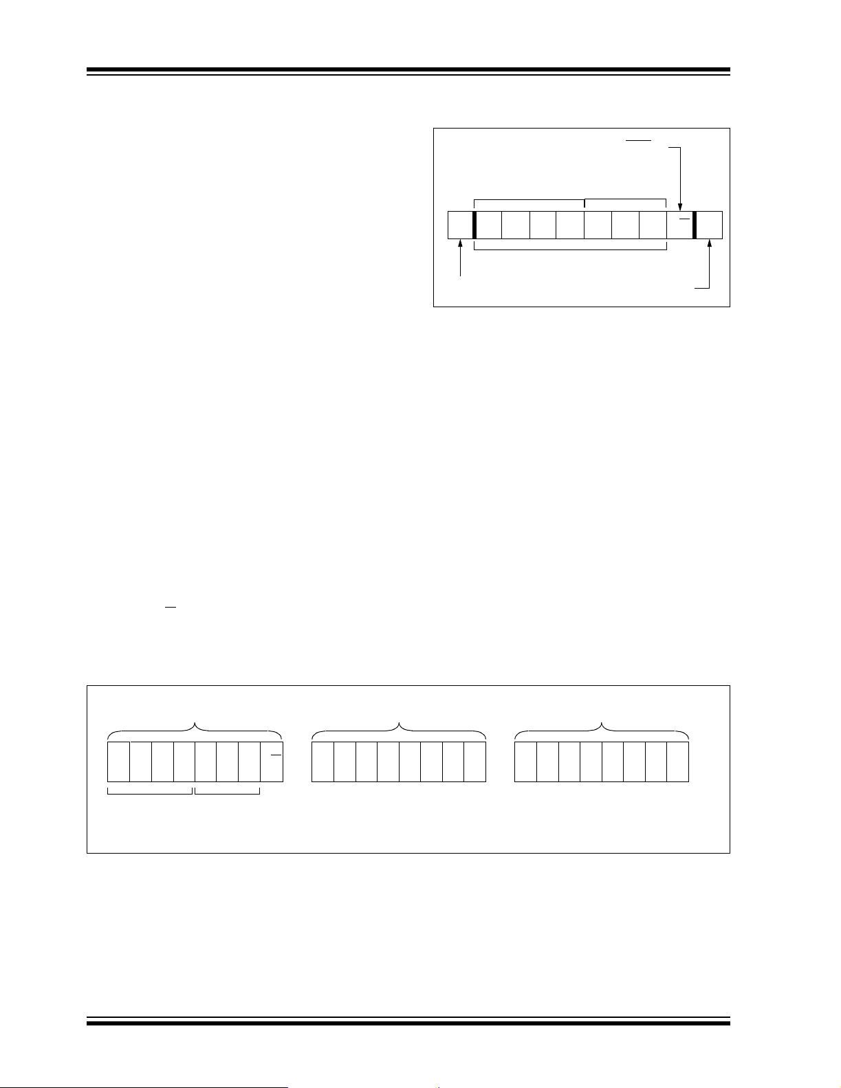
7.0 ACKNOWLEDGE POLLING
Since the device will not acknowledge during a write
cycle, this can be used to determine when the cycle is
complete (This feature can be used to maximize bus
throughput). Once the Stop condition for a Write
command has been issu ed from the mas ter , the device
initiates the internally timed write cycle. ACK polling
can be initiated immediately. This involves the master
sending a Start condition, followed by the control byte
for a Write command (R/W
busy with the write cycle, then no ACK will be returned.
If no ACK is returned, the S tart bit an d control byte must
be resent. If the cycle is complete, then the device will
return the ACK and the master can then proceed with
the next Read or Write command. See Figure 7-1 for
flow diagram.
= 0). If the device is still
FIGURE 7-1: ACKNOWLEDGE
POLLING FLOW
Send
Write Command
Send Stop
Condition to
Initiate Write Cycle
Send Start
Send Contr ol Byte
with R/W = 0
Did Device
Acknowledge
(ACK = 0)?
YES
NO
Next
Operation
DS21203N-page 10 © 2005 Microchip Technology Inc.
Page 11

24AA256/24LC256/24FC256
8.0 READ OPERATION
Read operations are ini tiated i n much the s ame way as
write operations, with the exception that the R/W
the control byte is set to ‘
1’. There are three basic types
of read operations: current addr ess read , rand om rea d
and sequential read.
8.1 Current Address Read
The 24XX256 contains an address counter that maintains the address of the last word accessed, internally
incremented by ‘
access was to address ‘n’ (n is any legal address), the
next current address read operati on would access da ta
from address n + 1.
Upon receipt of the control byte with R/W
the 24XX256 issu es an ac knowledge and tran smits the
8-bit data word. The master will not acknowledge the
transfer, but does generate a Stop condition and the
24XX256 discontinues transmission (Figure 8-1).
FIGURE 8-1: CURRENT ADDRESS
Bus Activity
Master
SDA Line
Bus Activity
1’. Therefore, if the previous read
READ
S
T
Control
A
R
T
1100
Byte
AAA
210
1
Data
Byte
A
C
K
bit of
bit set to ‘1’,
S
T
O
P
PS
N
O
A
C
K
8.2 Random Read
Random read operations allow the master to access
any memory location in a random manner. To perform
this type of read operatio n, th e w ord add res s mus t firs t
be set. This is d one by sending the word a ddress to th e
24XX256 as part of a write operation (R/W
0’). Once the word address is sent, the master gener-
‘
bit set to
ates a Start condition following the acknowledge. This
terminates the write operation, but not before the
internal Address Pointe r is set. Th e mast er then i ssues
the control byte again, but wit h the R/W bit set to a one.
The 24XX256 will then issue an acknowledge and
transmit the 8-bit data word. The master will not
acknowledge the transfer, though it does generate a
Stop condition, which causes the 24XX256 to discontinue transmission (Figure 8-2). After a random Read
command, the interna l address counte r will po int to th e
address location following the one that was just read.
8.3 Sequential Read
Sequential reads are initiated in the same way as a
random read except that after the 24XX256 transmits
the first data byte, the master issues an acknowledge
as opposed to the Stop condition used in a random
read. This acknowledge directs the 24XX256 to
transmit the next sequentially addressed 8-bit word
(Figure 8-3). Following the final byte transmitted to the
master , the m aster w ill NOT generate an ackn owledg e,
but will generate a Stop condition. To provide sequential reads, the 24XX256 contains an internal Address
Pointer which is incremented by one at the completion
of each operation. This Address Pointer allows the
entire memory contents to be serially read during one
operation. The internal Address Pointer will
automatically roll over from address 7FFF to address
0000 if the master acknowledges the byte received
from the array address 7FFF.
FIGURE 8-2: RANDOM READ
Bus Activity
Master
SDA Line
Bus Activity
x = “don’t care” bit
S
T
Control
A
Byte
R
T
S 1010
AAA
210
Address
High Byte
x
0
A
C
K
A
C
K
Address
Low Byte
S
T
A
R
T
S 1010
A
C
K
Control
Byte
AAA
210
Data
Byte
1
A
C
K
S
T
O
P
P
N
O
A
C
FIGURE 8-3: SEQUENTIAL READ
Bus Activity
Master
SDA Line
Bus Activity
© 2005 Microchip Technology Inc. DS21203N-page 11
Control
Byte
Data (n) Data (n + 1)
A
C
K
A
C
K
A
C
K
Data (n + 2)
Data (n + x)
A
C
K
S
T
O
P
P
N
O
A
C
K
Page 12

24AA256/24LC256/24FC256
9.0 PACKAGING INFORMATION
9.1 Package Marking Information
8-Lead PDIP (300 mil)
XXXXXXXX
T/XXXNNN
YYWW
8-Lead SOIC (150 mil)
XXXXXXXX
T/XXYYWW
NNN
8-Lead SOIC (208 mil)
XXXXXXXX
T/XXXXXX
YYWWNNN
Example:
24AA256
I/P 017
3
e
0510
Example:
24LC256I
3
e
SN 0510
017
Example:
24LC256
e
I/SM
0510017
3
Legend: XX...X Part number or part number code
T Temperature (I, E)
Y Year code (last digit of calendar year)
YY Year code (last 2 digits of calendar year)
WW Week code (week of January 1 is week ‘01’)
NNN Alphanumeric traceability code (2 characters for small packages)
Pb-free JEDEC designator for Matte Tin (Sn)
3
e
Note: For very small packages with no room for the Pb-free JEDEC designator
, the marking will only appear on the outer carton or reel label.
3
e
Note: In the event the full Microchip part numbe r cannot be ma rked on on e line, i t will
be carried over to the next line, thus limiting the number of available
characters for customer-specific information.
*St andard device mar king consi sts of Microch ip part num ber , year code, wee k code, and traceab ility code. For
device marking beyond this, certain price adders apply. Please check with your Microchip Sales Office.
DS21203N-page 12 © 2005 Microchip Technology Inc.
Page 13

24AA256/24LC256/24FC256
Package Marking Information (Continued)
8-Lead TSSOP
XXXX
TYWW
NNN
8-Lead MSOP Example:
XXXXXT
YWWNNN
8-Lead DFN-S
XXXXXXX
T/XXXXX
YYWW
NNN
Example:
4L256I
510017
Example
24LC256
I/MF
0510
017
4LD
I510
017
:
3
e
First Line Marking Codes
TSSOP Package Codes MSOP Package Codes
Part No.
24AA256 4AD 4A256T
24LC256 4LD 4L256T
24FC256 4FD 4F256T
© 2005 Microchip Technology Inc. DS21203N-page 13
Page 14

24AA256/24LC256/24FC256
8-Lead Plastic Dual In-line (P) – 300 mil (PDIP)
E1
D
2
n
E
β
eB
Number of Pins
Pitch
Top to Seating Plane A .140 .155 .170 3.56 3.94 4.32
Molded Package Thickness A2 .115 .130 .145 2.92 3.30 3.68
Base to Seating Plane A1 .015 0.38
Shoulder to Shoulder Width E .300 .313 .325 7.62 7.94 8.26
Molded Package Width E1 .240 .250 .260 6.10 6.35 6.60
Overall Length D .360 .373 .385 9.14 9.46 9.78
Tip to Seating Plane L .125 .130 .135 3.18 3.30 3.43
Lead Thickness
Upper Lead Width B1 .045 .058 .070 1.14 1.46 1.78
Lower Lead Width B .014 .018 .022 0.36 0.46 0.56
Overall Row Spacing § eB .310 .370 .430 7.87 9.40 10.92
Mold Draft Angle Top
Mold Draft Angle Bottom
* Controlling Parameter
§ Significant Characteristic
Notes:
Dimensions D and E1 do not include mold flash or protrusions. Mold flash or protrusions shall not exceed
.010” (0.254mm) per side.
JEDEC Equivalent: MS-001
Drawing No. C04-018
Dimension Limits MIN NOM MAX MIN NOM MAX
1
α
A
c
Units INCHES* MILLIMETERS
n
p
c
α
β
.008 .012 .015 0.20 0.29 0.38
A1
B1
B
88
.100 2.54
51015 51015
51015 51015
A2
L
p
DS21203N-page 14 © 2005 Microchip Technology Inc.
Page 15

24AA256/24LC256/24FC256
8-Lead Plastic Small Outline (SN) – Narrow, 150 mil (SOIC)
E
E1
p
D
2
B
Number of Pins
Pitch
Standoff §
Foot Angle
Lead Thickness
Mold Draft Angle Top
Mold Draft Angle Bottom
* Controlling Parameter
§ Significant Characteristic
Notes:
Dimensions D and E1 do not include mold flash or protrusions. Mold flash or protrusions shall not exceed
.010” (0.254mm) per side.
JEDEC Equivalent: MS-012
Drawing No. C04-057
n
45°
c
β
n
p
A1
φ
c
α
β
1
h
A
φ
L
048048
A1
MILLIMETERSINCHES*Units
1.27.050
α
A2
MAXNOMMINMAXNOMMINDimension Limits
88
1.751.551.35.069.061.053AOverall Height
1.551.421.32.061.056.052A2Molded Package Thickness
0.250.180.10.010.007.004
6.206.025.79.244.237.228EOverall Width
3.993.913.71.157.154.146E1Molded Package Width
5.004.904.80.197.193.189DOverall Length
0.510.380.25.020.015.010hChamfer Distance
0.760.620.48.030.025.019LFoot Length
0.250.230.20.010.009.008
0.510.420.33.020.017.013BLead Width
1512015120
1512015120
© 2005 Microchip Technology Inc. DS21203N-page 15
Page 16

24AA256/24LC256/24FC256
8-Lead Plastic Small Outline (SM) – Medium, 208 mil (SOIC)
E
E1
p
D
2
n
B
c
β
Number of Pins
Pitch
Foot Angle
Lead Thickne ss
Mold Draft Angle Top
Mold Draft Angle Bottom
* Controlling Parameter
§ Significant Characteristic
Notes:
Dimensions D and E1 do not include mold flash or protrusions. Mold flash or protrusions shall not exceed
.010” (0.254mm) per side.
Drawing No. C04-056
n
p
φ
c
α
β
1
A
φ
L
.070 .075
.069 .074
048048
A1
1.78
1.75
MILLIMETERSINCHES*Units
1.27.050
1.97
1.88
α
A2
MAXNOMMINMAXNOMMINDimension Limits
88
2.03.080AOverall Height
1.98.078A2Molded Package Thickness
0.250.130.05.010.005.002A1Standoff §
8.267.957.62.325.313.300EOverall Width
5.385.285.11.212.208.201E1Molded Package Width
5.335.215.13.210.205.202DOverall Length
0.760.640.51.030.025.020LFoot Length
0.250.230.20.010.009.008
0.510.430.36.020.017.014BLead Width
1512015120
1512015120
DS21203N-page 16 © 2005 Microchip Technology Inc.
Page 17

24AA256/24LC256/24FC256
8-Lead Plastic Thin Shrink Small Outline (ST) – 4.4 mm (TSSOP)
E
E1
p
D
2
n
B
1
A
c
A1
φ
β
Units
A1
n
p
φ
c
α
β
048048
Number of Pins
Pitch
Standoff §
Foot Angle
Lead Thickne ss
Mold Draft Angle Top
Mold Draft Angle Bottom
* Controlling Parameter
§ Significant Characteristic
Notes:
Dimensions D and E1 do not include mold flash or protrusions. Mold flash or protrusions shall not exceed
.005” (0.127mm) per side.
JEDEC Equivalent: MO-153
Drawing No. C04-086
L
MILLIMETERS*INCHES
0.65.026
α
A2
MAXNOMMINMAXNOMMINDimension Limits
88
1.10.043AOverall Height
0.950.900.85.037.035.033A2Mold ed Pa ckag e Thick ness
0.150.100.05.006.004.002
6.506.386.25.256.251.246EOverall Width
4.504.404.30.177.173.169E1Mold ed Pa ckag e Width
3.103.002.90.122.118.114DMolded Package Length
0.700.600.50.028.024.020LFoot Length
0.200.150.09.008.006.004
0.300.250.19.012.010.007BLead Width
10501050
10501050
© 2005 Microchip Technology Inc. DS21203N-page 17
Page 18

24AA256/24LC256/24FC256
8-Lead Plastic Micro Small Outline Package (MS) (MSOP)
E
E1
p
D
2
B
n 1
α
A
c
(F)
β
Units
Dimension Limits
Number of Pins
Pitch
Overall Height
Molded Package Thickness
Standoff
Overall Width
Molded Package Width
Overall Length
Foot Length
Foot Angle
Lead Thickness
Lead Width
Mold Draft Angle Top
Mold Draft Angle Bottom
*Controlling Parameter
Notes:
Dimensions D and E1 do not include mold flash or protrusions. Mold flash or protrusions shall not
exceed .010" (0.254mm) per side.
JEDEC Equivalent: MO-187
Drawing No. C04-111
A2
A1
E1
MIN
n
p
A
E
D
L
φ
c
B
α
β
.026 BSC
.030
.000
.193 TYP.
.118 BSC
.118 BSC
.016 .024
.037 REFFFootprint (Reference)
0° - 8°
.003
.009
5°
5° -
L
INCHES
NOM
.033
.006
.012
φ
A1
MAX NOM
8
--
-
-
.043
.037
.006
.031
.009
.016
15°
15°
MIN
0.75
0.00
0.40
0.08
0.22
MILLIMETERS*
MAX
8
0.65 BSC
--
0.85
-
4.90 BSC
3.00 BSC
3.00 BSC
0.60
0.95 REF
0°
-
-
-
A2
1.10
0.95
0.15
0.80
8°
0.23
0.40
15°5° 15°5° -
DS21203N-page 18 © 2005 Microchip Technology Inc.
Page 19

24AA256/24LC256/24FC256
8-Lead Plastic Dual Flat No Lead Package (MF) 6x5 mm Body (DFN-S)
A1
n
12
TOP VIEW
α
E1
E
B
R
D1 D
EXPOSED
METAL
PADS
BOTTOM VIEW
A2
A3
A
p
L
D2
PIN 1
ID
E2
Units
Dimension Limits
Number of Pins
Pitch
Overall Height
Molded Package Thickness
Standoff
Base Thickness
Overall Length
Molded Package Length
Exposed Pad Length
Molded Package Width
Exposed Pad Width D2 .085 .091 .097 2.16 2.31 2.46
Lead Width
Lead Length
Tie Bar Width
Mold Draft Angle Top
*Controlling Parameter
Notes:
Dimensions D and E1 do not include mold flash or protrusions. Mold flash or protrusions shall not exceed .010” (0.254mm) per side.
JEDEC equivalent: pending
Drawing No. C04-113
n
p
A
A2
A1
A3
E
E1
E2
DOverall Width
D1
B
L
R
α
MIN
INCHES
NOM
.050 BSC
.033
.026
.000
.152 .158 .163 3.85 4.00 4.15
.014
.020
.0004
.008 REF.
.194 BSC
.184 BSC
.236 BSC
.226 BSC
.016
.024
.014
MAX MIN
8
.039
.031
.002
.019
.030
12
MILLIMETERS*
1.27 BSC
0.00
0.20 REF.
4.92 BSC
4.67 BSC
5.99 BSC
5.74 BSC
0.35
0.50
0.85
0.65
0.01
0.40
0.60
.356
MAXNOM
8
1.00
0.80
0.05
0.47
0.75
12
© 2005 Microchip Technology Inc. DS21203N-page 19
Page 20

24AA256/24LC256/24FC256
APPENDIX A: REVISION HISTORY
Revision L
Corrections to Section 1.0, Electrical Characteristics.
Revision M
Added 1.8V 400 kHz option for 24FC256.
Revision N
Revised Sections 2.1 and 2.4. Removed 14-Lead
TSSOP Package.
DS21203N-page 20 © 2005 Microchip Technology Inc.
Page 21

24AA256/24LC256/24FC256
THE MICROCHIP WEB SITE
Microchip provides onlin e support v ia our W WW site at
www.m ic roc hi p.c om . Thi s web si te i s us ed as a m ean s
to make files and information easily available to
customers. Accessible by using your favorite Internet
browser, the web site contains the following
information:
• Product Support – Data sheets and errata,
application notes and sample programs, design
resources, user’s guides and hardware support
documents, lat est softwa re releases and archived
software
• General Technical Support – Frequently Asked
Questions (FAQ), technical support requests,
online discussion groups, Microchip consultan t
program member listing
• Business of Microchip – Product selector and
ordering guides, latest Microchip press releases,
listing of s eminars and events, listings of
Microchip sales offices, distributors and factory
representatives
CUSTOMER CHANGE NOTIFICATION SERVICE
CUSTOMER SUPPORT
Users of Microchip products can receive assistance
through several channels:
• Distributor or Representative
• Local Sal es Office
• Field Application Engineer (FAE)
• Technical Support
• Development Systems Information Line
Customers should contact their distributor,
representative or field application engineer (FAE) for
support. Local sales offices are also available to help
customers. A listing of sales offices and locations is
included in the back of this document.
T echnic al support is avail able throug h the web si te
at: http://support.microchip.com
Microchip’s customer notification service helps keep
customers current on Microchip products. Subscribers
will receive e-mail notification whenever there are
changes, updates, revisions or errata related to a
specified produ ct family or develo pment tool of inte rest.
To register, access the Microchip web site at
www.microchip.com, click on Customer Change
Notification and follow the registration instructions.
© 2005 Microchip Technology Inc. DS21203N-page 21
Page 22

24AA256/24LC256/24FC256
READER RESPONSE
It is our intentio n to pro vi de you with the best documentation possible to ens ure suc c es sfu l u se of y ou r M ic roc hip product. If you wish to provid e your c omment s on org anizatio n, clarity, subject matter, and ways in w hich o ur docum entatio n
can better serve you, please FAX your comments to the Technical Publications Manager at (480) 792-4150.
Please list the following information, and use this outline to provide us with your comments about this document.
To:
RE: Reader Response
From:
Application (optional):
Would you like a reply? Y N
Device: Literature Number:
Questions:
1. What are the best features of this document?
2. How does this document meet your hardware and software development needs?
3. Do you find the organization of this document easy to follow? If not, why?
Technical Publications Manager
Name
Company
Address
City / State / ZIP / Country
Telephone: (_______) _________ - _________
Total Pages Sent ________
FAX: (______) _________ - _________
DS21203N24AA256/24LC256/24FC256
4. What additions to the document do you think would enhance the structure and subject?
5. What deletions from the document could be made without affecting the overall usefulness?
6. Is there any incorrect or misleading information (what and where)?
7. How would you improve this document?
DS21203N-page 22 © 2005 Microchip Technology Inc.
Page 23

24AA256/24LC256/24FC256
PRODUCT IDENTIFICATION SYSTEM
To order or obtain information, e.g., on pricing or delivery, refer to the factory or the listed sales office.
PART NO. X /XX
Device
Device: 24AA256: 256 Kbit 1.8V I2C Serial
Temperature
Range:
Package: P = Plastic DIP (300 mil body), 8-lead
Lead Finish: Blank= Pb-free – Matte Tin (see Note 1)
Range
24AA256T: 256 Kbit 1.8V I2C Serial
24LC256: 256 Kbit 2.5V I2C Serial
24LC256T: 256 Kbit 2.5V I
24FC256: 256 Kbit High Speed I2C Serial
24FC256T: 256 Kbit High Speed I2C Serial
I= -40°C to +85°C
E= -40°C to +125°C
SN = Plastic SOIC (150 mil body), 8-lead
SM = Plastic SOIC (208 mil body), 8-lead
ST = Plastic TSSOP (4.4 mm), 8-lead
MF = Dual, Flat, No Lead (DFN)(6x5 mm
body), 8-lead
MS = Plastic Micro Small Outline (MSOP),
G = Pb-free – Matte Tin only
PackageTemperature
EEPROM
EEPROM Tape and Reel)
EEPROM
EEPROM Tape and Reel)
EEPROM
EEPROM Tape and Reel)
8-lead
2
C Serial
Finish
X
Lead
Examples:
a) 24AA256-I/P: Industrial Temp.,
1.8V, PDIP package.
b) 24AA256T-I/SN: Tape and Reel,
Industrial Temp., 1.8V, SOIC
package.
c) 24AA256-I/ST: Industrial Temp.,
1.8V, TSSOP package.
d) 24AA256-I/MS: Industrial Temp.,
1.8V, MSOP package.
e) 24LC256-E/P: Extended Temp.,
2.5V, PDIP package.
f) 24LC256-I/SN: Industrial Temp.,
2.5V, SOIC package.
g) 24LC256T-I/SN: Tape and Reel,
Industrial Temp., 2.5V, SOIC
package.
h) 24LC256-I/MS: Industrial Temp,
2.5V, MSOP package.
i) 24FC256-I/P: Industrial Temp,
1.8V, High Speed, PDIP package.
j) 24FC256-I/SN: Industrial Temp,
1.8V, High Speed, SOIC package.
k) 24FC256T-I/SN: Tape and Reel,
Industrial Temp, 1.8V, High Speed,
SOIC package
l) 24LC256T-I/STG:Industrial Temp,
2.5V , TSSOP pack age, T ape & R eel,
Pb-free
m) 24LC256-I/PG: Industrial Temp,
2.5V, PDIP package, Pb-free
Note 1: Most products manufactured after January 2005 will have a Matte Tin (Pb-free) finish. Most products
manufactured befor e January 2 005 will h ave a fin ish of ap proximately 63% S n and 37% Pb ( Sn/Pb). Ple ase
visit www.microchip.com for the latest inform ati on on Pb-fre e c onv ers ion , in clu di ng c onv ersio n date codes.
Sales and Support
Data Sheets
Products supported by a preliminary Data Sheet may have an errata sheet describing minor operational differences
and recommended workarounds. To determine if an errata sheet exists for a particular device, please contact one of
the following:
1. Your local Microchip sales office
2. The Microchip Corporate Literature Center U.S. FAX: (480) 792-7277
3. The Microchip Worldwide Site (www.microchip.com)
Please specify which device, revision of silicon and Data Sheet (include Literature #) you are using.
New Customer Notification System
Register on our web site (www.microchip.com/cn) to receive the most current information on our products.
© 2005 Microchip Technology Inc. DS21203N-page 23
Page 24

24AA256/24LC256/24FC256
NOTES:
DS21203N-page 24 © 2005 Microchip Technology Inc.
Page 25

Note the following details of the code protection feature on Microchip devices:
• Microchip products meet the specification contained in their particular Microchip Data Sheet.
• Microchip believes that its family of products is one of the most secure families of its kind on the market t oday, when used in the
intended manner and under normal conditions.
• There are dishonest and possibly illegal methods used to breach the code protection feature. All of these methods, to our
knowledge, require using the Microchip products in a manner outside the operating specifications contained in Microchip’s Data
Sheets. Most likely, the person doing so is engaged in theft of intellectual property.
• Microchip is willing to work with the customer who is concerned about the integrity of their code.
• Neither Microchip nor any other semiconductor manufacturer can guarantee the security of their code. Code protection does not
mean that we are guaranteeing the product as “unbreakable.”
Code protection is constantly evolving. We at Microchip are com mitted to continuously improving the code protect ion f eatures of our
products. Attempts to break Microchip’s code protection feature may be a violation of the Digit al Mill ennium Copyright Act. If such acts
allow unauthorized access to your software or other copyrighted work, you may have a right to sue for relief under that Act.
Information contained in this publication regarding device
applications and the like is provided only for your convenience
and may be superseded by updates. It is your responsibility to
ensure that your application meets with your specifications.
MICROCHIP MAKES NO REPRESENTATIONS OR WARRANTIES OF ANY KIND WHETHER EXPRESS OR IMPLIED,
WRITTEN OR ORAL, STATUTORY OR OTHERWISE,
RELATED TO THE INFORMATION, INCLUDING BUT NOT
LIMITED TO ITS CONDITION, QUALITY, PERFORMANCE,
MERCHANTABILITY OR FITNESS FOR PURPOSE.
Microchip disclaims all liability arising from this information and
its use. Use of M icrochip’s prod ucts as critical components in
life support systems is not authorized except with express
written approval by Microchip. No licenses are conveyed,
implicitly or otherwise, under any Microchip intellectual property
rights.
Trademarks
The Microchip name and logo, the Microchip logo, Accuron,
dsPIC, K
EELOQ, microID, MPLAB, PIC, PICmicro, PICSTART,
PRO MATE, PowerSmart, rfPIC, and SmartShunt are
registered trademarks of Microchip Technology Incorporated
in the U.S.A. and other countries.
AmpLab, FilterLab, Migratable Memory, MXDEV, MXLAB,
PICMASTER, SEEVAL, SmartSensor and The Embedded
Control Solutions Company are registered trademarks of
Microchip Technology Incorporated in the U.S.A.
Analog-for-the-Digital Age, Application Maestro, dsPICDEM,
dsPICDEM.net, dsPICworks, ECAN, ECONOMONITOR,
FanSense, FlexROM, fuzzyLAB, In-Circuit Serial
Programming, ICSP, ICEPIC, Linear Active Thermistor,
MPASM, MPLIB, MPLI NK, MPSIM, PICkit , PICDEM,
PICDEM.net, PICLAB, PICtail, PowerCal, PowerInfo,
PowerMate, PowerTool, rfLAB, rfPICDEM, Select Mode,
Smart Serial, SmartTel, Total Endurance and WiperLock are
trademarks of Microchip Technology Incorporated in the
U.S.A. and other countries.
SQTP is a service mark of Microchip T echnology Incorporated
in the U.S.A.
All other trademarks mentioned herein are property of their
respective companies.
© 2005, Microchip Technology Incorporated, Printed in the
U.S.A., All Rights Reserved.
Printed on recycled paper.
Microchip received ISO/TS-16949:2002 quality system certification for
its worldwide headquarters, design and wafer fabrication facilities in
Chandler and Tempe, Arizona and Mountain View, California in
October 2003. The Company’s quality system processes and
procedures are for its PICmicro
devices, Serial EEPROMs, microperipherals, nonvolatile memory and
analog products. In addition, Microchip’s quality system for the design
and manufacture of development systems is ISO 9001:2000 certified.
®
8-bit MCUs, KEELOQ
®
code hopping
© 2005 Microchip Technology Inc. DS21203N-page 25
Page 26

WORLDWIDE SALES AND SERVICE
AMERICAS
Corporate Office
2355 West Chandler Blvd.
Chandler, AZ 85224-6199
Tel: 480-792-7200
Fax: 480-792-7277
Technical Support:
http://support.microchip.com
Web Address:
www.microchip.com
Atlanta
Alpharetta, GA
Tel: 770-640-0034
Fax: 770-640-0307
Boston
Westborough, MA
Tel: 774-760-0087
Fax: 774-760-0088
Chicago
Itasca, IL
Tel: 630-285-0071
Fax: 630-285-0075
Dallas
Addison, TX
Tel: 972-818-7423
Fax: 972-818-2924
Detroit
Farmington Hills, MI
Tel: 248-538-2250
Fax: 248-538-2260
Kokomo
Kokomo, IN
Tel: 765-864-8360
Fax: 765-864-8387
Los Angeles
Mission Viejo, CA
Tel: 949-462-9523
Fax: 949-462-9608
San Jose
Mountain View, CA
Tel: 650-215-1444
Fax: 650-961-0286
Toronto
Mississauga, Ontario,
Canada
Tel: 905-673-0699
Fax: 905-673-6509
ASIA/PACIFIC
Australia - Sydney
Tel: 61-2-9868-6733
Fax: 61-2-9868-6755
China - Beijing
Tel: 86-10-8528-2100
Fax: 86-10-8528-2104
China - Chengdu
Tel: 86-28-8676-6200
Fax: 86-28-8676-6599
China - Fuzhou
Tel: 86-591-8750-3506
Fax: 86-591-8750-3521
China - Hong Kong SAR
Tel: 852-2401-1200
Fax: 852-2401-3431
China - Qingdao
Tel: 86-532-8502-7355
Fax: 86-532-8502-7205
China - Shanghai
Tel: 86-21-5407-5533
Fax: 86-21-5407-5066
China - Shenyang
Tel: 86-24-2334-2829
Fax: 86-24-2334-2393
China - Shenzhen
Tel: 86-755-8203-2660
Fax: 86-755-8203-1760
China - Shunde
Tel: 86-757-2839-5507
Fax: 86-757-2839-5571
China - Wuhan
Tel: 86-27-5980-5300
Fax: 86-27-5980-5118
China - Xian
Tel: 86-29-8833-7250
Fax: 86-29-8833-7256
ASIA/PACIFIC
India - Bangalore
Tel: 91-80-2229-0061
Fax: 91-80-2229-0062
India - New Delhi
Tel: 91-11-5160-8631
Fax: 91-11-5160-8632
India - Pune
Tel: 91-20-2566-1512
Fax: 91-20-2566-1513
Japan - Yokohama
Tel: 81-45-471- 6166
Fax: 81-45-471-6122
Korea - Gumi
Tel: 82-54-473-4301
Fax: 82-54-473-4302
Korea - Seoul
Tel: 82-2-554-7200
Fax: 82-2-558-5932 or
82-2-558-5934
Malaysia - Penang
Tel: 604-646-8870
Fax: 604-646-5086
Philippines - Manila
Tel: 632-634-9065
Fax: 632-634-9069
Singapore
Tel: 65-6334-8870
Fax: 65-6334-8850
Taiwan - Hsin Chu
Tel: 886-3-572-9526
Fax: 886-3-572-6459
Taiwan - Kaohsiung
Tel: 886-7-536-4818
Fax: 886-7-536-4803
Taiwan - Taipei
Tel: 886-2-2500-6610
Fax: 886-2-2508-0102
Thailand - Bangkok
Tel: 66-2-694-1351
Fax: 66-2-694-1350
EUROPE
Austria - Weis
Tel: 43-7242-2244-399
Fax: 43-7242-2244-393
Denmark - Copenhagen
Tel: 45-4450-2828
Fax: 45-4485-2829
France - Paris
Tel: 33-1-69-53-63-20
Fax: 33-1-69-30-90-79
Germany - Munich
Tel: 49-89-627-144-0
Fax: 49-89-627-144-44
Italy - Milan
Tel: 39-0331-742611
Fax: 39-0331-466781
Netherlands - Drunen
Tel: 31-416-690399
Fax: 31-416-690340
Spain - Madrid
Tel: 34-91-352-30-52
Fax: 34-91-352-11-47
UK - Wokingham
Tel: 44-118-921-5869
Fax: 44-118-921-5820
08/24/05
DS21203N-page 26 © 2005 Microchip Technology Inc.
 Loading...