

24AA024/24LC024/24AA025/24LC025
L
A
2K I2C™ Serial EEPROM
Device Selection Table
Part
Number
24AA024 1.7V-5.5V 400 kHz
24AA025 1.7V-5.5V 400 kHz
24LC024 2.5V-5.5V 400 kHz I Yes
24LC025 2.5V-5.5V 400 kHz I No
Note 1: 100 kHz for V
VCC
Range
Max
Clock
CC < 2.5V
Temp.
Range
(1)
IYes
(1)
INo
Write
Protect
Features:
• Single supply with op eration from 1.7 V to 5.5 V for
24AA024/24AA025 device s, 2.5V for 24LC024/
24LC025 devices
• Low-power CMOS technology:
- Read current 1 mA, typical
- Standby current 1 μA, typical
• 2-wire serial interface, I
• Cascadable up to eight devices
• Schmitt Trigger inputs for noise suppression
• Output slope control to eliminate ground bounce
• 100 kHz and 400 kHz clock compatibility
• Page write time 5 ms maximu m
• Self-timed erase/write cycle
• 16-byte page write buffer
• Hardware write-protect on 24XX024 devices
• ESD protection >4,000V
• More than 1 million erase/write cycles
• Data retention >200 years
• Factory programming available
• Packages include 8-lead PDIP, SOIC, TSSOP,
DFN and MSOP
• Pb-free and RoHS compliant
• Temperature ranges:
- Industrial (I): -40°C to +85°C
2
C™ compatible
Description:
The Microchip Technology Inc. 24AA024/24LC024/
24AA025/24LC025 is a 2 Kbit Serial Electrically
Erasable PROM with a voltage range of 1.7V to 5.5V.
The device is organi zed as a singl e block of 256 x8-bit
memory with a 2-wire serial interface. Low current
design permits operation with typical standby and
active currents of only 1 μA and 1 mA, respectively.
The device has a page write capability for up to 16
bytes of data. Functional address lines allow the
connection of up to eight 24AA024/24LC024/
24AA025/24LC025 devices on the same bus for up to
16K bits of contiguous EEPROM memory. The device
is available in the standard 8-pin PDIP, 8-pin SOIC
(3.90 mm), TSSOP, 2x3 DFN and MSOP packages.
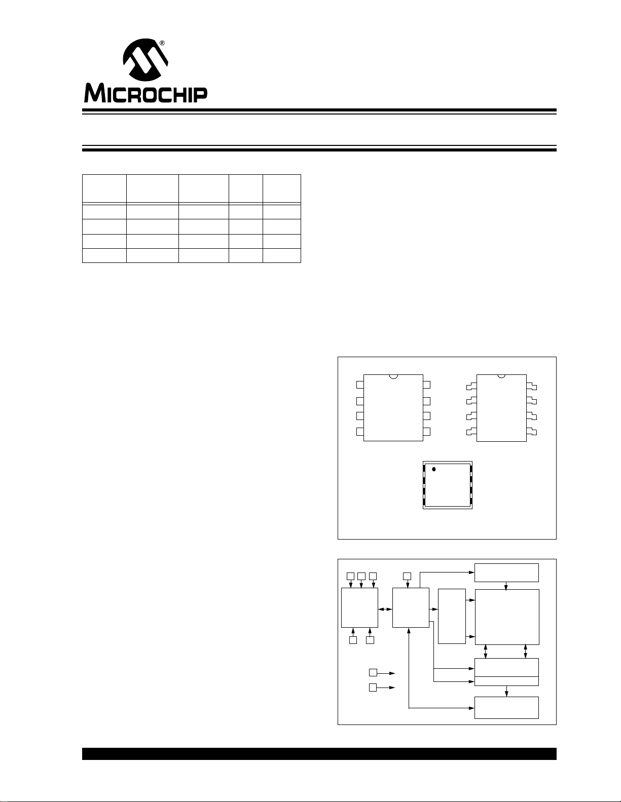
Package Types
A0
A1
A2
V
SS
8
7
6
5
SOIC, TSSOP
1
2
3
4
V
CC
WP
SCL
SDA
8
V
CC
7
WP
6
SC
5
SD
PDIP, MSOP
1
A0
2
A1
3
A2
4
SS
V
Note: WP pin is not internally connected on the
A0
A1
A2
V
SS
24XX025
8
VCC
WP
7
SCL
6
SDA
5
DFN
1
2
3
4
.
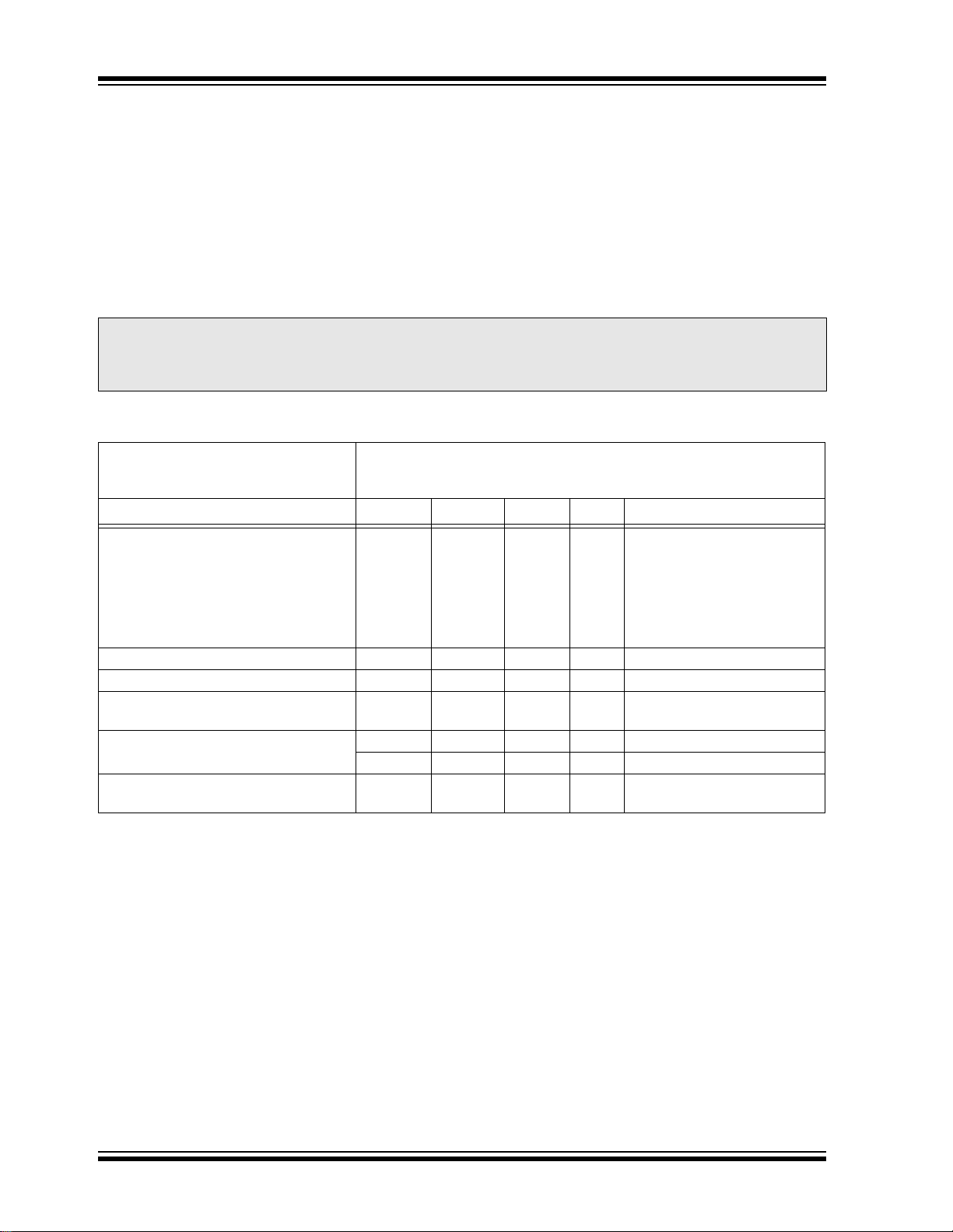
Block Diagram
A0 A1 A2
I/O
Control
Logic
WP*
Memory
Control
Logic
HV Generator
XDEC
EEPROM
Array
SDA
SCL
CC
© 2007 Microchip Technology Inc. DS21210K-page 1
V
VSS
Write-Protect
Circuitry
YDEC
Sense Amp.
R/W Control
24AA024/24LC024/24AA025/24LC025
1.0 ELECTRICAL CHARACTERISTICS
Absolute Maximum Ratings
VCC.............................................................................................................................................................................6.5V
All inputs and outputs w.r.t. V
Storage temperature ...............................................................................................................................-65°C to +150°C
Ambient temperature with power applied................................................................................................-40°C to +125°C
ESD protection on all pins ......................................................................................................................................................≥ 4 kV
† NOTICE: Stresses above those listed under “Absolute Maximum Ratings” may cause permanent damage to the
device. This is a stres s ratin g only and func tional operati on of the devic e at thos e or any other co nditio ns abov e thos e
indicated in the operational listings of this specification is not implied. Exposure to maximum rating conditions for
extended periods may affect device reliability.
SS .........................................................................................................-0.6V to VCC +1.0V
(†)
TABLE 1-1: DC CHARACTERISTICS
All parameters apply across the
specified operating ranges unless
otherwise noted.
Parameter Symbol Min. Max. Units Conditions
SCL and SDA pins:
High-level input voltage VIH 0.7 VCC —V—
Low-level input voltage VIL — 0.3 VCC V—
Hysteresis of Schmitt Trigger inputs V
Low-level output voltage VOL —0.40VIOL = 3.0 mA, VCC = 4.5V
Input leakage current I
Output leakage current ILO —±1μAVOUT = VSS or VCC
Pin capacitance (all inputs/outputs) CIN, COUT —10pFVCC = 5.0V (Note)
Operating current ICC Read — 1 mA VCC = 5.5V, SCL = 400 kHz
Standby current I
Note: This parameter is periodically sampled and not 100% tested.
CC = 1.7V to 5.5V
V
Industrial (I): T
HYS 0.05 VCC —V(Note)
LI —±1μAVIN = VSS or VCC
ICC Write — 3 mA VCC = 5.5V
CCS —1μAVCC = 5.5V, SDA = SCL = VCC
A = -40°C to +85°C
OL = 2.1 mA, VCC = 2.5V
I
T
A = 25°C, FCLK = 1 MHz
WP = V
SS, A0, A1, A2 = VSS
DS21210K-page 2 © 2007 Microchip Technology Inc.
24AA024/24LC024/24AA025/24LC025
TABLE 1-2: AC CHARACTERISTICS
All parameters apply across the specified
operating ranges unless otherwise noted.
V
CC = 1.7V to 5.5V
Industrial (I): T
A = -40°C to +85°C
Parameter Symbol
STD MODE
Vcc = 2.5V - 5.5V
FAST MODE
Units Remarks
Min. Max. Min. Max.
Clock frequency F
CLK — 100 — 400 kHz —
Clock high time THIGH 4000 — 600 — ns —
Clock low time TLOW 4700 — 1300 — ns —
SDA and SCL rise time T
R — 1000 — 300 ns (Note 1)
SDA and SCL fall time TF — 300 — 300 ns (Note 1)
Start condition hold time THD:STA 4000 — 600 — ns After this period the first
clock pulse is generated
Start condition setup time T
SU:STA 4700 — 600 — ns Only relevant for repeated
Start condition
Data input hold time T
HD:DAT 0—0—ns(Note 2)
Data input setup time TSU:DAT 250 — 100 — ns —
Stop condition setup time TSU:STO 4000 — 600 — ns —
Output valid from clock T
AA — 3500 — 900 ns (Note 2)
Bus free time TBUF 4700 — 1300 — ns Time the bus must be free
before a new transmission
can start
Output fall time from VIH
minimum to VIL maximum
Input filter spik e s upp res si on
T
OF — 250 20 +0.1
B
C
T
SP — 50 — 50 ns (Note 3)
250 ns (Note 1), CB ≤ 100 pF
(SDA and SCL pins)
Write cycle time T
WC — 5 — 5 ms Byte or Page mode
Endurance 1M — 1M — cycles 25°C, (Note 4)
Note 1: Not 100% tested. C
B = total capacitance of one bus line in pF.
2: As a transmitter, the device must provide an internal minimum delay time to bridge the undefined region
(minimum 300 ns) of the falling edge of SCL to avoid unintended generation of Start or Stop conditions.
3: The combined T
SP and VHYS specifications are due to Schmitt Trigger inputs which provide improved
noise spike suppression. This eliminates the need for a TI specification for standard operation.
4: This parameter is not tested but ensured by characterization. For endurance estimates in a specific
application, please consult the Total Endurance™ Model which can be downloaded at
www.microchip.com.
© 2007 Microchip Technology Inc. DS21210K-page 3
24AA024/24LC024/24AA025/24LC025
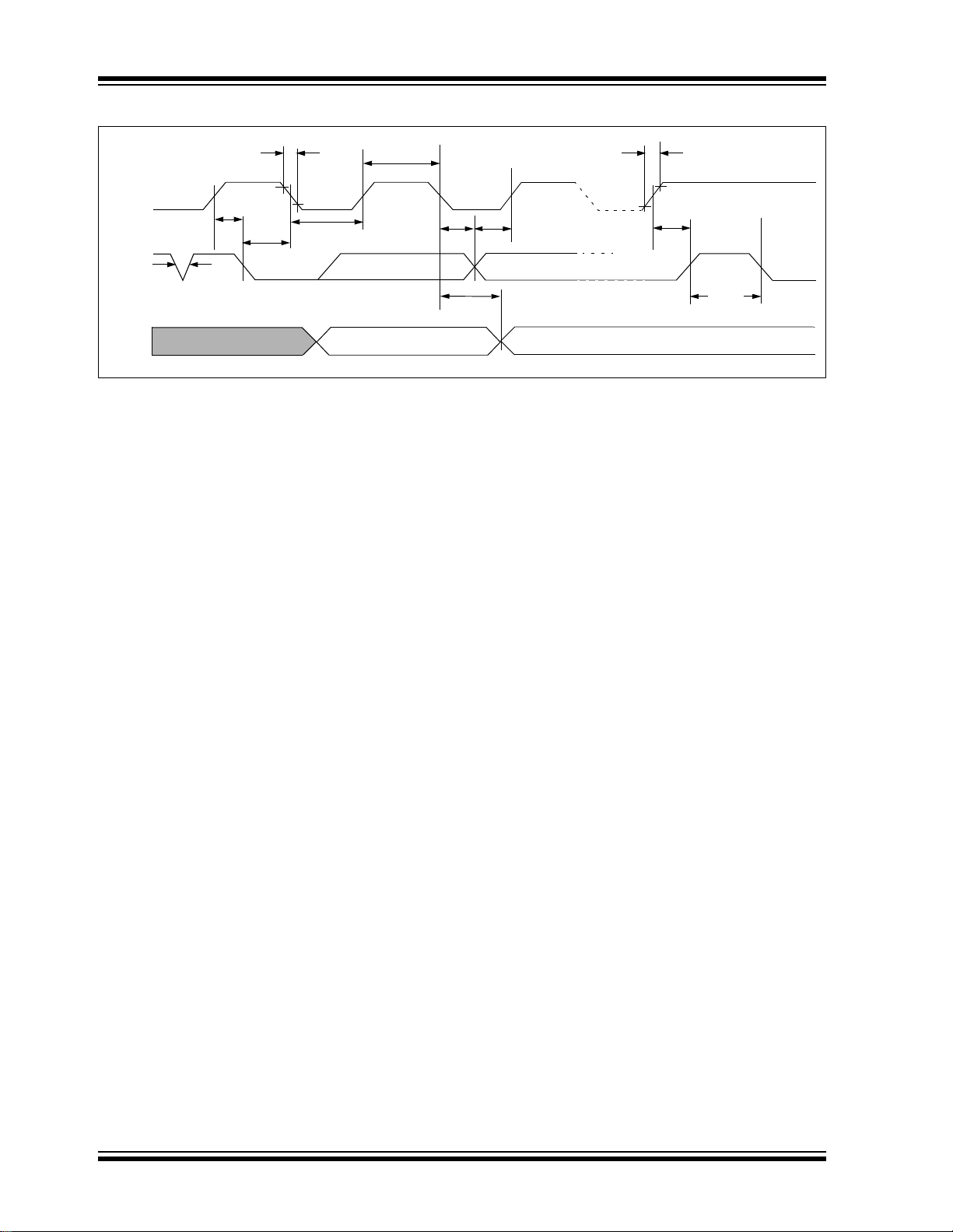
FIGURE 1-1: BUS TIMING DATA
SCL
SDA
IN
SDA
OUT
TSU:STA
TSP
TF
THD:STA
TLOW
THIGH
THD:DAT TSU:DAT TSU:STO
TAA
TR
TBUF
DS21210K-page 4 © 2007 Microchip Technology Inc.

24AA024/24LC024/24AA025/24LC025
2.0 PIN DESCRIPTIONS
Pin Function Table
Name PDIP SOIC TSSOP DFN MSOP Description
A01111 1 Address Pin AO
A12222 2 Address Pin A1
A23333 3 Address Pin A2
SS 4444 4 Ground
V
SDA5555 5 Serial Address/Data I/O
SCL6666 6 Serial Clock
WP7777 7 Write-Protect Input
CC 8888 8 +1.7 to 5.5V Power Supply
V
2.1 SDA Serial Data
SDA is a bidirectional pin used to transfer addresses
and data into and out of the device. It is an open-drain
terminal, therefore, the SDA bus requires a pull-up
resistor to V
400 kHz).
For normal data transfer, SDA is allowed to change
only during SCL low. Changes during SCL high are
reserved for indicating the Start and Stop conditions.
CC (typical 10 kΩ for 100 kHz, 2 kΩ for
2.2 SCL Serial Clock
The SCL input is used to sync hro ni ze th e da t a tra ns fer
from and to the device.
2.3 A0, A1, A2
The levels on the A0, A1 and A2 inputs are compared
with the corresponding bits in the slave address. The
chip is selected if the compare is true.
Up to eight 24AA024/24LC024/24AA025/24LC025
devices may be connected to the same bus by using
different Chip Select bit combinations. These inputs
must be connected to either V
CC or VSS.
2.4 WP (24XX024 Only)
2.5 Noise Protection
The 24AA024/24LC024/24AA025/24LC025 employs a
V
CC threshold detector circuit which disables the
internal erase/write logic if th e V
nominal conditions.
The SCL and SDA inputs have Schmitt Trigger and
filter circuits which suppress noise spikes to assure
proper device operation, even on a noisy bus.
CC is below 1.5 v olt s at
3.0 FUNCTIONAL DESCRIPTION
The 24AA024/24LC024/24AA025/24LC025 supports
a bidirectional, 2-wire bus and data transmission
protocol. A device that sends data onto the bus is
defined as transmitter, while a device receiving data
is defined as receiver. The bus has to be controlled
by a master device which generates the Serial Clock
(SCL), controls the bus access and generates the
Start and Stop conditions, while the 24AA024/
24LC024/24AA025/24LC025 works as slave. Both
master and slave can operate as transmitter or
receiver, but the master device determines which
mode is activated.
WP is the hardware write-protect pin. It must be tied to
V
CC or VSS. If tied to Vcc, hardware write protection is
enabled. If WP is tied to Vss, the hardware write
protection is disabled. Note that the WP pin is avail able
only on the 24XX024. This pin is not internally
connected on the 24LC025.
© 2007 Microchip Technology Inc. DS21210K-page 5
24AA024/24LC024/24AA025/24LC025
4.0 BUS CHARACTERISTICS
The following bus protocol has been defined:
• Data transfer may be initiated only when the bus
is not busy.
• During data transfer, the data line must remain
stable wheneve r the c lock lin e is high . Changes i n
the data line while the clock line is high will be
interpreted as a Start or Stop condition.
Accordingly, the following bus conditions have been
defined (Figure 4-1).
4.1 Bus Not Busy (A)
Both data and clock lines remain high.
4.2 Start Data Transfer (B)
A high-to-low transition of the SDA line while the clock
(SCL) is high determines a Start condition. All
commands must be preceded by a Start condition.
4.3 Stop Data Transfer (C)
A low-to-high transition of the SDA line while the clock
(SCL) is high determines a Stop condition. All
operations must be ended with a Stop condition.
4.4 Data Valid (D)
The state of the data line represents valid data when,
after a Start condition, the data line is stable for the
duration of the high period of the clock signal.
The data on the line must be changed during the low
period of the clock signal. There is one bit of data per
clock pulse.
Each data transfer is initiated with a S tart condition and
terminated with a Stop condition. The number of the
data bytes transferred between the Start and Stop
conditions is determined by the master device and is,
theoretically , u nlimited, (thoug h only the last six teen will
be stored when performin g a write ope ration). When an
overwrite does occur, it will replace data in a first-in
first-out fashion.
4.5 Acknowledge
Each receiving device, when addressed, is required to
generate an acknowledge after the reception of each
byte. The ma ster devi ce m ust gener at e an ex tr a cloc k
pulse which is associated with this Acknowledge bit.
Note: The 24AA024/24LC024/24AA025/24LC025
does not generate any Acknowledge bits if
an internal programming cycle is in
progress.
The device that acknowledges has to pull dow n the SDA
line during the acknowledge clock pulse in such a way
that the SDA line is stable low during the high period of
the acknowledge-related clock pulse. Of course, setup
and hold times must be taken into account. A master
must signal an end of data to the slave by not generating
an Acknowledge bit on the last byte that has been
clocked out of the slave. In this case, the slave must
leave the data line high to enable the master to generate
the Stop condition (Fi gure4-2).
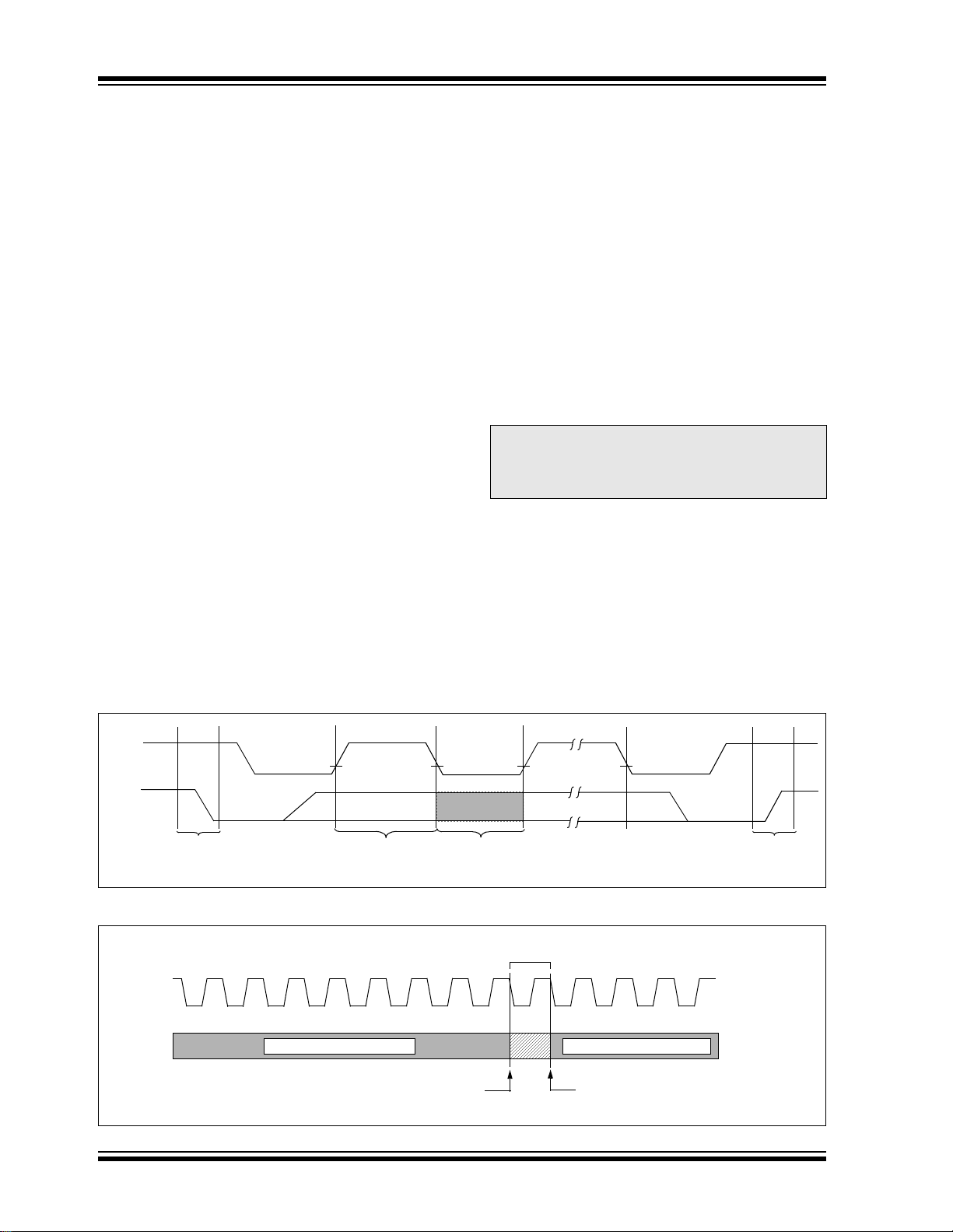
FIGURE 4-1: DAT A TRANSFER SEQUENCE ON THE SERIAL BUS CHARACTERISTICS
(A) (B) (C) (D) (A)(C)
SCL
SDA
Start
Condition
Address or
Acknowledge
Valid
Data
Allowed
to Change
FIGURE 4-2: ACKNOWLEDGE TIMING
Acknowledge
Bit
SCL
SDA
Transmitter must release the SDA line at this point allowing
the Receiver to pull the SDA line low to acknowledge the
previous eight bits of data.
987654321 123
Data from transmitterData from transmitter
Receiver must release the SDA line at this
point so the Transmitter can continue
sending data.
Stop
Condition
DS21210K-page 6 © 2007 Microchip Technology Inc.
24AA024/24LC024/24AA025/24LC025
5.0 DEVICE ADDRESSING
A control byte is the first byte received following the
Start condition from the master device (Figure 5-1).
The control byte co nsi sts of a four-bit control cod e. F or
the 24AA024/24LC024/24AA025/24LC025, this is set
as ‘1010’ binary for read and write operations. The next
three bits of the control byte are the Chip Select bits
(A2, A1, A0). The Chip Select bits allow the use of up
to eight 24AA024/24LC024/24AA025/24LC025
devices on the same bus and are used to select which
device is accessed. The Chip Select bits in the control
byte must correspond to the logic levels on the corresponding A2, A1 and A0 pins for the device to respon d.
These bits are in effect t he three Mos t Significant bits of
the word address.
The last bit of the control byte defines the operation to
be performed. When set to a one, a read operation is
selected. When set to a zero, a write operation is
selected. Following the Start condition, the 24AA024/
24LC024/24AA025/24LC025 monitors the SDA bus
checking the control byte being transmitted. Upon
receiving a ‘1010’ code and appropriate Chip Select
bits, the slave device outputs an Acknowledge signal
on the SDA line. Depending on the state of the R/W
the 24AA024/24LC024/24AA0 25/24LC025 wi ll select a
read or write operation.
bit,
FIGURE 5-1: CONTROL BYTE FORMAT
Start Bit
Read/Write
Chip Select
Control Code
101 0A2 A1 A0SACKR/W
Slave Address
Acknowledge Bit
Bit
Bits
5.1 Contiguous Addressing Across
Multiple Devices
The Chip Select bits A2, A1 and A0 can be used to
expand the co ntiguous address space for up to 16K bits
by adding up to eight 24AA024/24LC024/24AA025/
24LC025 devices on the same bus. In this case, software can use A0 of th e con tro l byt e as address bit A8,
A1 as address bit A9 and A2 as address bit A10. It is
not possible to sequentially read across device
boundaries.
© 2007 Microchip Technology Inc. DS21210K-page 7
24AA024/24LC024/24AA025/24LC025
6.0 WRITE OPERATIONS
6.1 Byte Write
Following the Start signal from the master, the device
code(4 bits), the Chip Select bits (3 bits) and theR/W
bit (which is a logic-low) is placed onto the bus by the
master transmitter. The device will acknowledge this
control byte during the ninth cloc k pulse. The ne xt byte
transmitte d by th e maste r is the word ad dr ess and w ill
be written into the Address Pointer of the 24AA024/
24LC024/24AA025/24LC025. After receiving another
Acknowledge signal from the 24AA024/24LC024/
24AA025/24LC025, the master device will transmit the
data word to be written into the addressed memory
location. The 24AA024/24LC024/24AA025/24LC025
acknowledges again and the master generates a Stop
condition. This ini tiates the interna l write cycle an d, during this time, the 24AA024/24LC024/24AA025/
24LC025 will not generate Acknowledge signals
(Figure 6-1). If an attempt is made to write to the
protected portion of the array when the hardware write
protection (24XX024 only) has been enabled, the
device will acknowledge the command, but no data will
be written. The write cycle time must be observed even
if write protection is enabled.
6.2 Page Write
The write control byte, word address and the first data
byte are transmitted to the 24AA024/24LC024/
24AA025/24LC025 in the same way as in a byte write.
However, instead of generating a Stop condition, the
master transmits up to 15 additional data bytes to the
24AA024/24LC024/24AA025/24LC025, which are
temporarily stored in the on-chip pa ge buffer and will be
written into the memory once the master has transmitted a Stop condition. Upon receipt of each word, the
four lower-order Address Pointer bits are internally
incremented by one.
The higher-order four bits of the word address remain
constant. If the master should transmit more than 16
bytes prior to generating the Stop condition, the
address counter will roll over and the previously
received data w ill be ov erwritten . As w ith t he by te-write
operation, once the Stop condition is received, an
internal write cycle wil l begin (Figure6-2). If an attempt
is made to write to the protected portion of the array
when the hardware write protection has been enabled,
the device will ack nowled ge th e comma nd, but no dat a
will be written. The write cycle time must be observed
even if write protection is enabled.
Note: Page write operations are limite d to writing
bytes within a single physical page,
regardless
of the number of bytes
actually being written. Physical page
boundaries start at addresses that are
integer multiples of the page buf fer size (or
‘page size’) an d end at addresses that are
integer multiples of [page size – 1]. If a
Page Write command attempts to write
across a physical page boundary, the
result is that the data wraps around to the
beginning of the current page (overwriting
data previously stored there), instead of
being written to the next page, as might b e
expected. It is therefore necessary for the
application software to prevent page write
operations that would attempt to cross a
page boundary.
6.3 Write Protection
The WP pin (available on 24XX024 only) must be tied
CC or VSS. If tie d to VCC, the entire array will be
to V
write-protected. If the WP pin is tied to V
operations to all address locations are allowed.
SS, write
FIGURE 6-1: BYTE WRITE
BUS ACTIVITY
MASTER
SDA LINE
BUS ACTIVITY
S
T
A
R
T
S P
Control
Byte
Word
Address
A
C
K
A
C
K
Data
S
T
O
P
A
C
K
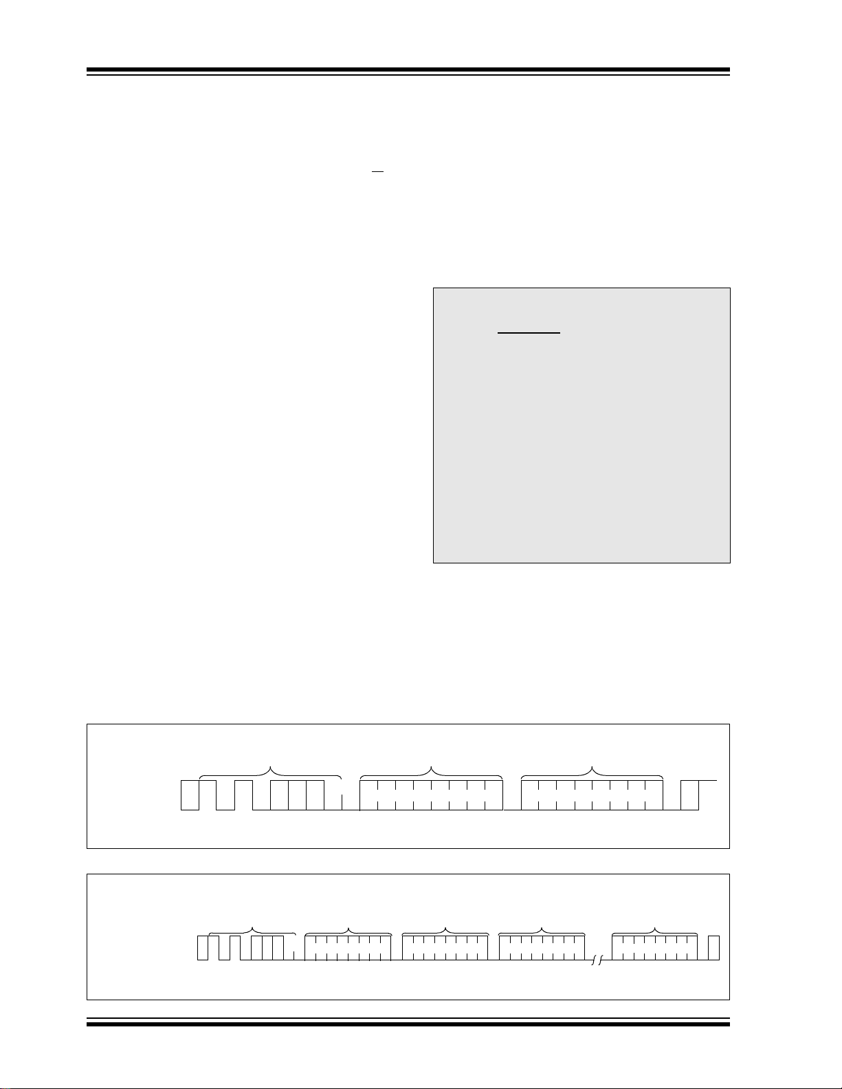
FIGURE 6-2: PAGE WRITE
S
BUS ACTIVITY
MASTER
SDA LINE
BUS ACTIVITY
DS21210K-page 8 © 2007 Microchip Technology Inc.
T
A
Control
R
T
S P
Byte
A
C
K
Word
Address
(n)
Data (n) Data (n + 15)
A
C
K
Data (n +1)
A
C
K
A
C
K
S
T
O
P
A
C
K

24AA024/24LC024/24AA025/24LC025
7.0 ACKNOWLEDGE POLLING
Since the device will not acknowledge during a write
cycle, this can be used to determine when the cycle is
complete (this feature can be used to maximize bus
throughput). Once the Stop condition for a Write
command has been issu ed from the mas ter , the device
initiates the internally-timed write cycle, with ACK
polling being initiated immediately. This involves the
master sending a S tart c ondition fo llowed by t he contro l
byte for a Write command (R/W
busy with the write cycl e, no ACK wil l be re turned. If no
ACK is returned, the Start bit and control byte must be
re-sent. If the cycle is complete, the device will return
the ACK and the mast er can then pro ceed with the next
Read or Write command. See Figure 7-1 for a flow
diagram of this operation.
= 0). If the device is still
FIGURE 7-1: ACKNOWLEDGE POLLING
FLOW
Send
Write Command
Send Stop
Condition to
Initiate Write Cycle
Send Start
Send Control Byte
with R/W
Acknowledge
(ACK = 0)?
= 0
Did Device
Yes
No
Next
Operation
© 2007 Microchip Technology Inc. DS21210K-page 9

24AA024/24LC024/24AA025/24LC025
8.0 READ OPERATIONS
Read operations are initiated in the same way as write
operations, with the exception that the R/W
slave address is set to ‘1’. There are three basic types
of read operations: current add ress read , rand om rea d
and sequential read.
8.1 Current Address Read
The 24AA024/24LC024/24AA025/24LC025 contains
an address counter that maintains the address of the
last word accessed, internally incremented by one.
Therefore, if the previous read access was to address
n, the next current address read operation would
access data from address n + 1. Upon receipt of the
slave address with the R/W
bit set to ‘1’, the 24AA024/
24LC024/24AA025/24LC025 issues an acknowledge
and transmits the 8-bit data word. The master will not
acknowledge the transfer, but does generate a Stop
condition and the 24AA024/24LC024/24AA025/
24LC025 discontinues transmission (Figure 8-1).
8.2 Random Read
Random read operations allow the master to access
any memory location in a random manner. To perform
this type of read operatio n, th e w ord add ress m us t firs t
be set. This is accomplished by sending the word
address to th e 24AA024/2 4LC024/24A A025/24LC 025
as part of a write operation. Once the word address is
sent, the master generates a Start condition following
the acknowledge. This terminates the write operation,
but not before the internal Address Pointer is set. The
master then issues the control byte again, but with the
bit set to a ‘1’. The 24AA024/24L C024 /2 4AA0 25/
R/W
24LC025 will th en issue an ack nowledge a nd transm its
the eight bit data word. The master will not acknowledge the transfer but does generate a Stop condition
and the 24AA024/24LC024/24AA025/24LC025
discontinues transmission (Figure 8-2). After this
command, the interna l addre ss co unter wil l point to th e
address location following the one that was just read.
bit of the
8.3 Sequential Read
Sequential reads are initiated in the same way as a
random read except that after the 24AA024/24LC024/
24AA025/24LC025 transmits the first data byte, the
master issues an acknowledge (as opposed to a Stop
condition in a random read). This di rect s the 24AA02 4/
24LC024/24AA025/24LC025 to transmit the next
sequentially-addressed 8-bit word (Figure 8-3).
To provide sequential reads, the 24AA024/24LC024/
24AA025/24LC025 contains an internal Address
Pointer that is incremented by one upon completion of
each operation. This Address Pointer allows the entire
memory contents to be serially read during one
operation. The internal Address Pointer will
automatically roll over from address 0FFh to address
000h.
FIGURE 8-1: CURRENT ADDRESS
READ
BUS ACTIVITY
MASTER
SDA LINE
BUS ACTIVITY
S
T
Control
A
Byte
R
T
S
Data
A
C
K
S
T
O
P
P
N
O
A
C
K
DS21210K-page 10 © 2007 Microchip Technology Inc.
24AA024/24LC024/24AA025/24LC025
FIGURE 8-2: RANDOM READ
S
BUS ACTIVITY
MASTER
SDA LINE
BUS ACTIVITY
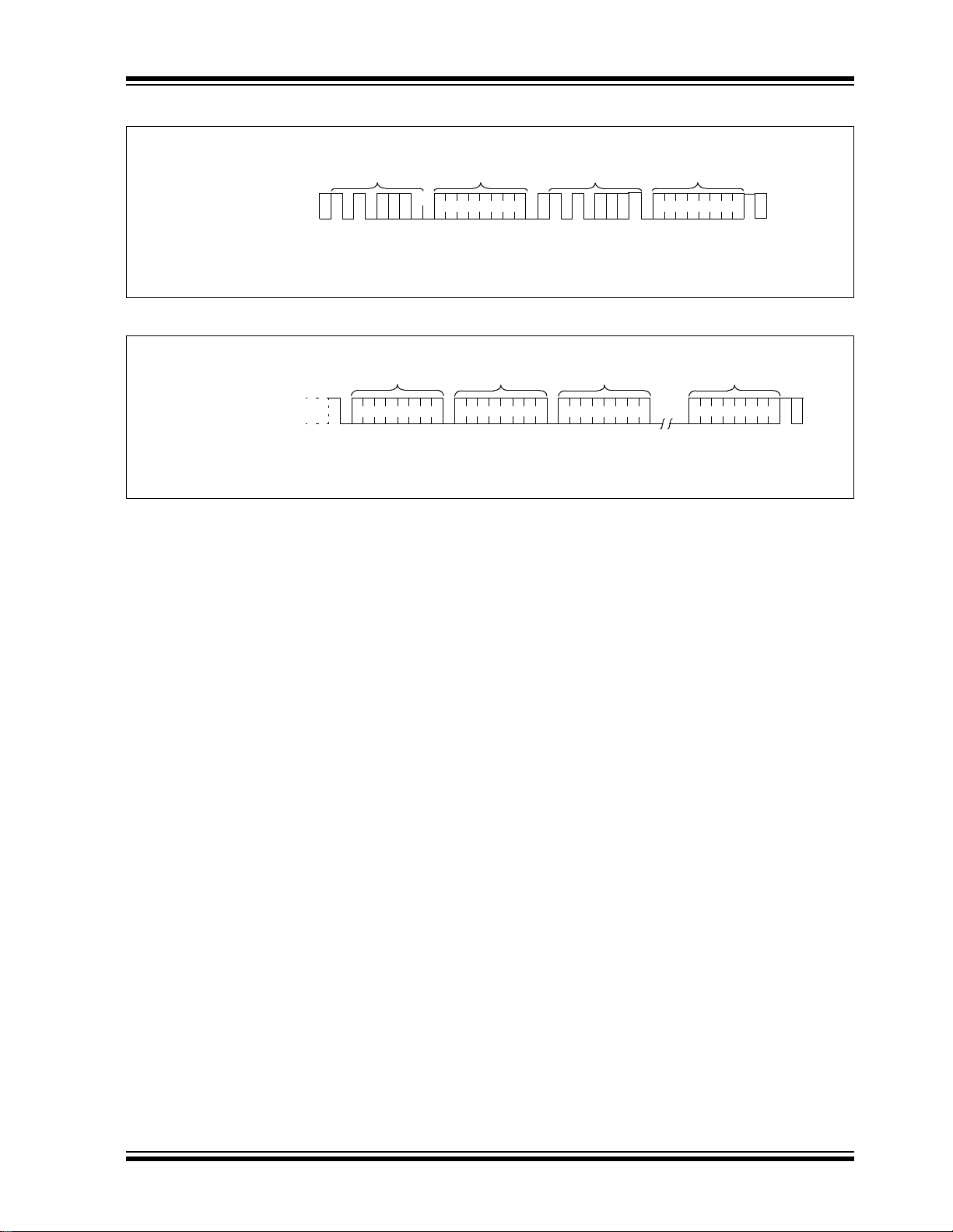
FIGURE 8-3 : SEQUENTIAL REA D
T
Control
A
Byte
R
T
S P
Address (n)
A
C
K
Word
S
T
Control
A
Byte
R
T
S
A
C
K
A
C
K
Data (n)
S
T
O
P
N
O
A
C
K
BUS ACTIVITY
MASTER
SDA LINE
BUS ACTIVITY
Control
Byte
Data (n) Data (n + 1) Data (n + 2) Data (n + x)
A
C
K
A
C
K
A
C
K
A
C
K
S
T
O
P
P
N
O
A
C
K
© 2007 Microchip Technology Inc. DS21210K-page 11

24AA024/24LC024/24AA025/24LC025
9.0 PACKAGING INFORMATION
9.1 Package Marking Information
8-Lead PDIP (300 mil)
XXXXXXXX
T/XXXNNN
YYWW
8-Lead SOIC (3.90 mm)
XXXXXXXT
XXXXYYWW
NNN
8-Lead TSSOP
XXXX
TYWW
NNN
Example:
24LC024
I/P 13F
3
e
0519
Example:
24LC024I
SN 0519
3
e
13F
Example:
4L24
I519
13F
8-Lead MSOP
XXXXT
YWWNNN
8-Lead 2x3 DFN
XXX
YWW
NN
Example:
4L24I
51913F
Example:
2P4
519
13
DS21210K-page 12 © 2007 Microchip Technology Inc.

24AA024/24LC024/24AA025/24LC025
l
Part Number
24AA024 4A24 4A24T 2P1
24LC024 4L24 4L24T 2P4
24AA025 4A25 4A25T 2R1
24LC025 4L25 4L25T 2R4
Note: T = Temperature grade (I, E)
Legend: XX...X Part number or part number code
T Temperature (I, E)
Y Year code (last digit of calendar year)
YY Year code (last 2 digits of calendar year)
WW Week code (week of January 1 is week ‘01’)
NNN Alphanumeric traceability code (2 characters for small packages)
Pb-free JEDEC designator for Matte Tin (Sn)
Note: For very small packages with no room for the Pb-free JEDEC designator
, the marking will only appear on the outer carton or reel label.
3
e
Note: In th e event th e full Mi croch ip pa rt numbe r canno t be ma rked on one line , it wil
be carried over to the next line, thus limiting the number of available
characters for customer-specific information.
1st Line Marking Codes
TSSOP MSOP DFN
3
e
Note: Please visit www.microchip.com/Pbfree for the latest information on Pb-free conversion.
*Standard OTP marking consists of Microchip part number, year code, week code, and traceability code.
© 2007 Microchip Technology Inc. DS21210K-page 13

24AA024/24LC024/24AA025/24LC025
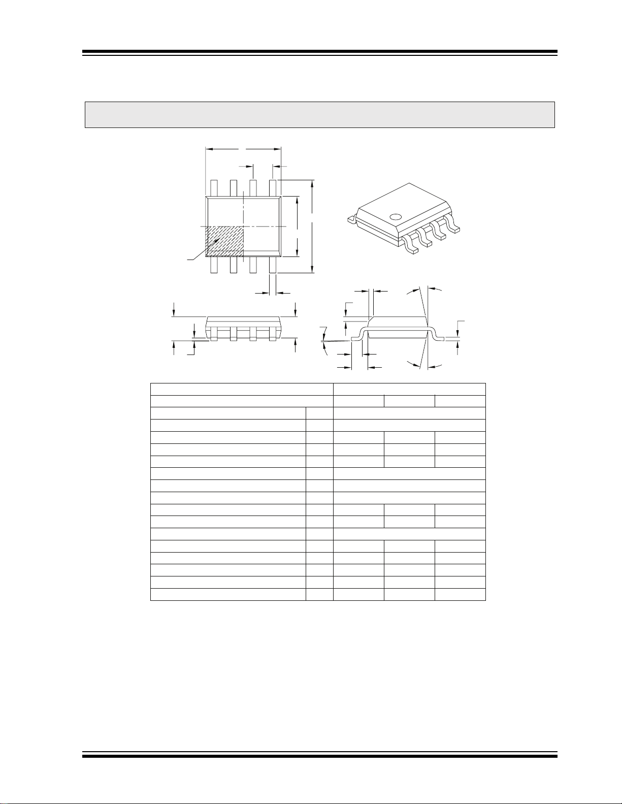
8-Lead Plastic Dual In-Line (P or PA) – 300 mil Body [PDIP]
N
1
2
3
4
B
Note: For the most current package drawings, please see the Microchip Packaging Specification located at
http://www.microchip.com/packaging
N
otes:
. Pin 1 visual index feature may vary, but must be located with the hatched area.
. § Significant Characteristic.
. Dimensions D and E1 do not include mold flash or protrusions. Mold flash or protrusions shall not exceed .010" per side.
. Dimensioning and tolerancing per ASME Y14.5M.
BSC: Basic Dimension. Theoretically exact value shown without tolerances.
NOTE 1
E1
12
A
A1
b1
b
Number of Pins N 8
Pitch e .100 BSC
Top to Seating Plane A – – .210
Molded Package Thickness A2 .115 .130 .195
Base to Seating Plane A1 .015 – –
Shoulder to Shoulder Width E .290 .310 .325
Molded Package Width E1 .240 .250 .280
Overall Length D .348 .365 .400
Tip to Seating Plane L . 115 .130 .150
Lead Thickness c .008 . 010 .015
Upper Lead Width b1 .040 .060 .070
Lower Lead Width b .014 .018 .022
Overall Row Spacing § eB – – .430
3
D
L
e
Units INCHES
Dimension Limits MIN NOM MAX
E
A2
c
eB
Microchip Technology Drawing C04-018
DS21210K-page 14 © 2007 Microchip Technology Inc.
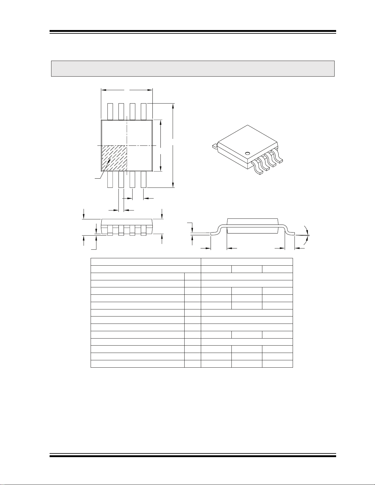
24AA024/24LC024/24AA025/24LC025
8-Lead Plastic Small Outline (SN or OA) – Narrow, 3.90 mm Body [SOIC]
B
Note: For the most current package drawings, please see the Microchip Packaging Specification located at
http://www.microchip.com/packaging
D
e
N
E
E1
NOTE 1
12 3
b
h
h
α
φ
A
A1
A2
L
L1
β
c
Units MILLIMETERS
Dimension Limits MIN NOM MAX
Number of Pins N 8
Pitch e 1.27 BSC
Overall Height A – – 1.75
Molded Package Thickness A2 1.25 – –
Standoff
§
A1 0.10 – 0.25
Overall Width E 6.00 BSC
Molded Package Width E1 3.90 BSC
Overall Length D 4.90 BSC
Chamfer (optional) h 0.25 – 0.50
Foot Length L 0.40 – 1.27
Footprint L1 1.04 REF
Foot Angle φ 0° – 8°
Lead Thickness c 0.17 – 0.25
Lead Width b 0.31 – 0.51
Mold Draft Angle Top α 5° – 15°
Mold Draft Angle Bottom β 5° – 15°
Notes:
1. Pin 1 visual index feature may vary, but must be located within the hatched area.
2. § Significant Characteristic.
3. Dimensions D and E1 do not include mold flash or protrusions. Mold flash or protrusions shall not exceed 0.15 mm per side.
4. Dimensioning and tolerancing per ASME Y14.5M.
BSC: Basic Dimension. Theoretically exact value shown without tolerances.
REF: Reference Dimension, usually without tolerance, for information purposes only.
Microchip Technology Drawing C04-057
© 2007 Microchip Technology Inc. DS21210K-page 15

24AA024/24LC024/24AA025/24LC025
8-Lead Plastic Thin Shrink Small Outline (ST) – 4.4 mm Body [TSSOP]
N
1
2
3
B
Note: For the most current package drawings, please see the Microchip Packaging Specification located at
http://www.microchip.com/packaging
D
N
E
E1
NOTE 1
12
b
e
c
A
A1
Number of Pins N 8
Pitch e 0.65 BSC
Overall Height A – – 1.20
Molded Package Thickness A2 0.80 1.00 1.05
Standoff A1 0.05 – 0.15
Overall Width E 6.40 BSC
Molded Package Width E1 4.30 4.40 4.50
Molded Package Length D 2.90 3.00 3.10
Foot Length L 0.45 0.60 0.75
Footprint L1 1.00 REF
Foot Angle φ 0° – 8°
Lead Thickness c 0.09 – 0.20
Lead Width b 0.19 – 0.30
otes:
. Pin 1 visual index feature may vary, but must be located within the hatched area.
. Dimensions D and E1 do not include mold flash or protrusions. Mold flash or protrusions shall not exceed 0.15 mm per side.
. Dimensioning and tolerancing per ASME Y14.5M.
BSC: Basic Dimension. Theoretically exact value shown without tolerances.
REF: Reference Dimension, usually without tolerance, for information purposes only.
A2
L1
Units MILLIMETERS
Dimension Limits MIN NOM MAX
L
φ
Microchip Technology Drawing C04-086
DS21210K-page 16 © 2007 Microchip Technology Inc.
24AA024/24LC024/24AA025/24LC025
8-Lead Plastic Micro Small Outline Package (MS or UA) [MSOP]
B
Note: For the most current package drawings, please see the Microchip Packaging Specification located at
http://www.microchip.com/packaging
D
N
E
E1
NOTE 1
2
1
e
b
A
A1
Number of Pins N 8
Pitch e 0.65 BSC
Overall Height A – – 1.10
Molded Package Thickness A2 0.75 0.85 0.95
Standoff A1 0.00 – 0.15
Overall Width E 4.90 BSC
Molded Package Width E1 3.00 BSC
Overall Length D 3.00 BSC
Foot Length L 0.40 0.60 0.80
Footprint L1 0.95 REF
Foot Angle φ 0° – 8°
Lead Thickness c 0.08 – 0.23
Lead Width b 0.22 – 0.40
Notes:
1. Pin 1 visual index feature may vary, but must be located within the hatched area.
2. Dimensions D and E1 do not include mold flash or protrusions. Mold flash or protrusions shall not exceed 0.15 mm per side.
3. Dimensioning and tolerancing per ASME Y14.5M.
BSC: Basic Dimension. Theoretically exact value shown without tolerances.
REF: Reference Dimension, usually without tolerance, for information purposes only.
A2
Dimension Limits MIN NOM MAX
c
L1
Units MILLIMETERS
Microchip Technology Drawing C04-111
φ
L
© 2007 Microchip Technology Inc. DS21210K-page 17
24AA024/24LC024/24AA025/24LC025
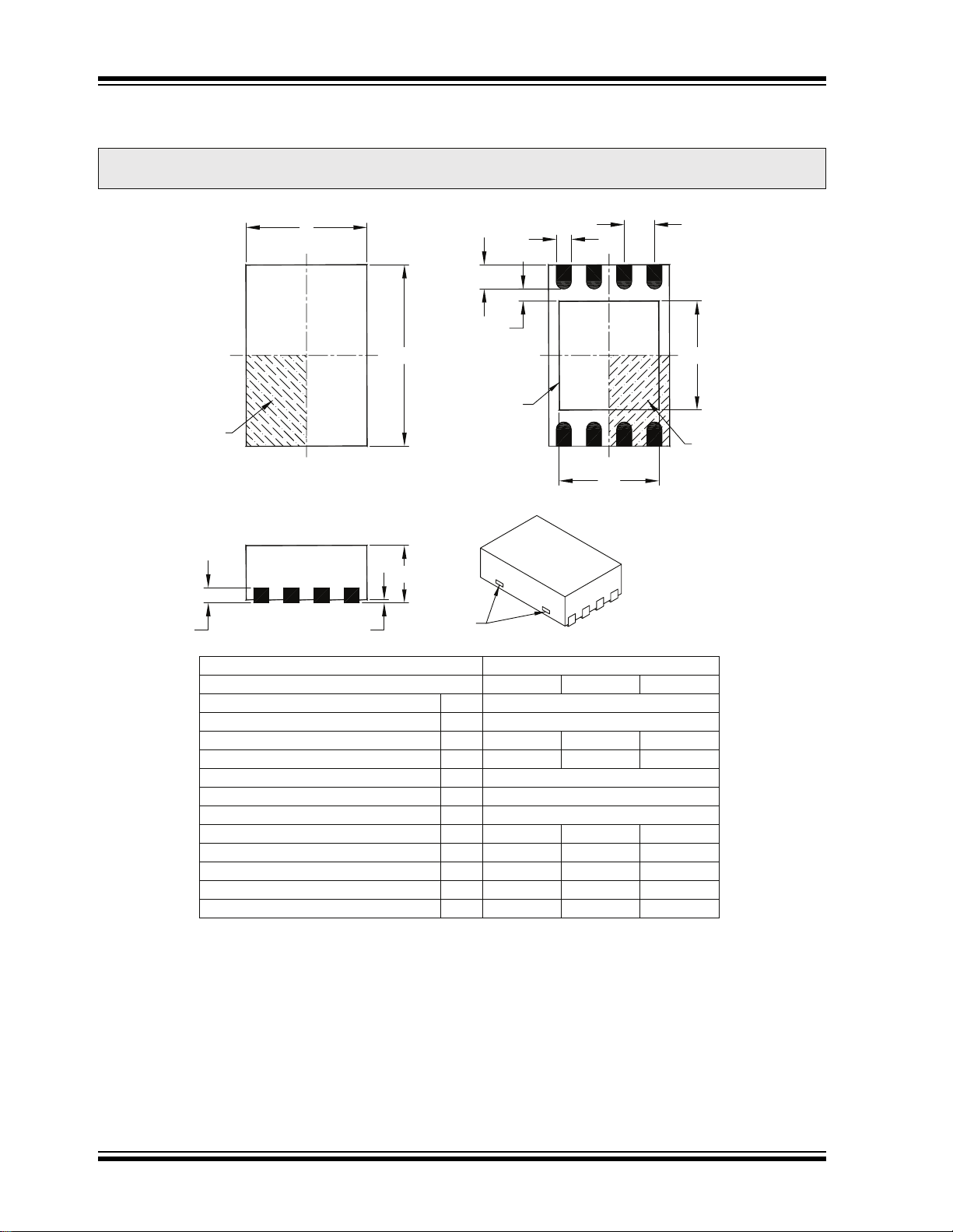
8-Lead Plastic Dual Flat, No Lead Package (MC) – 2x3x0.9 mm Body [DFN]
N
1
2
3
4
B
Note: For the most current package drawings, please see the Microchip Packaging Specification located at
http://www.microchip.com/packaging
D
N
L
b
K
E
EXPOSED PAD
NOTE 1
2
1
TOP VIEW
A
A3 A1
Number of Pins N 8
Pitch e 0.50 BSC
Overall Height A 0.80 0.90 1.00
Standoff A1 0.00 0.02 0.05
Contact Thickness A3 0. 20 REF
Overall Length D 2.00 BSC
Overall Width E 3.00 BSC
Exposed Pad Length D2 1.30 – 1.75
Exposed Pad Width E2 1.50 – 1.90
Contact Width b 0.18 0.25 0.30
Contact Length L 0.30 0.40 0.50
Contact-to-Exposed Pad K 0.20 – –
otes:
. Pin 1 visual index feature may vary, but must be located within the hatched area.
. Package may have one or more exposed tie bars at ends.
. Package is saw singulated.
. Dimensioning and tolerancing per ASME Y14.5M.
BSC: Basic Dimension. Theoretically exact value shown without tolerances.
REF: Reference Dimension, usually without tolerance, for information purposes only.
NOTE 2
Units MILLIMETERS
Dimension Limits MIN NOM MAX
BOTTOM VIEW
e
N
E2
1
2
D2
Microchip Technology Drawing C04-123
NOTE 1
DS21210K-page 18 © 2007 Microchip Technology Inc.

24AA024/24LC024/24AA025/24LC025
APPENDIX A: REVISION HISTORY
Revision F
Corrections to Section 1.0, Electrical Characteristics.
Revision G
Added part number 24AA025 to document.
Correction to Section 1.0, Ambient Temperature.
Revision H
Added DFN package.
Revision J (02/2007)
Revised Features sec tion; Revis ed Pin Function Table;
Changed 1.8V to 1.7V, Table 1-1 and Table 1-2;
Replaced Package Drawings; Replaced On-line
Support page; Revised Product ID section.
Revision K (03/2007)
Replaced Package Drawings (Rev. AM).
© 2007 Microchip Technology Inc. DS21210K-page 19

24AA024/24LC024/24AA025/24LC025
NOTES:
DS21210K-page 20 © 2007 Microchip Technology Inc.

24AA024/24LC024/24AA025/24LC025
THE MICROCHIP WEB SITE
Microchip provides onlin e support v ia our W WW site at
www.m ic roc hi p.c om . Thi s web si te i s us ed as a m ean s
to make files and information easily available to
customers. Accessible by using your favorite Internet
browser, the web site contains the following
information:
• Product Support – Data sheets and errata,
application notes and sample programs, design
resources, user’s guides and hardware support
documents, lat est softwa re releases and archived
software
• General Technical Support – Frequently Asked
Questions (FAQ), technical support requests,
online discussion groups, Microchip consultan t
program member listing
• Business of Microchip – Product selector and
ordering guides, latest Microchip press releases,
listing of s eminars and events, listings of
Microchip sales offices, distributors and factory
representatives
CUSTOMER CHANGE NOTIFICATION SERVICE
CUSTOMER SUPPORT
Users of Microchip products can receive assistance
through several channels:
• Distributor or Representative
• Local Sal es Office
• Field Application Engineer (FAE)
• Technical Support
• Development Systems Information Line
Customers should contact their distributor,
representative or field application engineer (FAE) for
support. Local sales offices are also available to help
customers. A listing of sales offices and locations is
included in the back of this document.
T echnic al support is avail able throug h the web si te
at: http://support.microchip.com
Microchip’s customer notification service helps keep
customers current on Microchip products. Subscribers
will receive e-mail notification whenever there are
changes, updates, revisions or errata related to a
specified produ ct family or develo pment tool of inte rest.
To register, access the Microchip web site at
www.microchip.com, click on Customer Change
Notification and follow the registration instructions.
© 2007 Microchip Technology Inc. DS 21210K-page 21

24AA024/24LC024/24AA025/24LC025
READER RESPONSE
It is our intentio n to pro vi de you with the best documentation possible to ens ure suc c es sfu l u se of y ou r M ic roc hip product. If you wish to provid e your c omment s on org anizatio n, clarity, subject matter , and ways in w hich o ur document atio n
can better serve you, please FAX your comments to the Technical Publications Manager at (480) 792-4150.
Please list the following information, and use this outline to provide us with your comments about this document.
To:
RE: Reader Response
From:
Application (optional):
Would you like a reply? Y N
Device: Literature Number:
Questions:
1. What are the be st features of this document?
2. How does this document meet your hardware and software development needs?
3. Do you find the organization of this document easy to follow? If not, why?
Technical Publications Manager
Name
Company
Address
City / State / ZIP / Country
Telephone: (_______) _________ - _________
Total Pages Sent ________
FAX: (______) _________ - _________
DS21210K24AA024/24LC024/24AA025/24LC025
4. What additions to the document do you think would enhance the structure and subject?
5. What deletions from the document could be made without affecting the overall usefulness?
6. Is there any incorrect or misleading information (what and where)?
7. How would you improve this document?
DS21210K-page 22 © 2007 Microchip Technology Inc.

24AA024/24LC024/24AA025/24LC025
PRODUCT IDENTIFICATION SYSTEM
To order or obtain information, e.g., on pricing or delivery, refer to the factory or the listed sales office.
PART NO. X /XX
Device
PackageTemperature
Range
Device: 24AA024: 1.7V, 2 Kbit Addressable Seria l EEPRO M with
24AA024T:1.7V, 2 Kbit Addressabl e Seri al EEP ROM
24LC024: 2.5V, 2Kbi t Addressa bl e Seri a l EEPRO M with
24LC024T:2.5V, 2 Kbit Addressa bl e Seri a l EEPRO M
24AA025: 1.7V, 2 Kbit Addressable Seria l EEPRO M with
24AA025T:1.7V, 2 Kbit Addressabl e Seri al EEP ROM
24LC025: 2.5V, 2Kbi t Addressa bl e Seri a l EEPRO M
24LC025T:2.5V, 2 Kbit Addressa bl e Seri a l EEPRO M
Temperature Range: I = -40°C to +85°C
WP pin.
(Tape and Reel) with WP pin.
WP pin.
(Tape and Reel) with WP pin.
no WP pin.
(Tape and Reel) with no WP pin.
(Tape and Reel) with no WP pin.
(Tape and Reel) with no WP pin.
Examples:
a) 24AA024-I/P: Industrial Temperature,
1.7V, PDIP Package
b) 24AA024-I/SN: Industrial Temperature,
1.7V, SOIC Package
c) 24AA025T-I/ST: Industrial Temperature,
1.7V, TSSOP Package, Tape and Reel,
no WP
d) 24LC024-I/P: Industrial Temperature,
2.5V, PDIP Package
e) 24LC024-I/MS: Industrial Temperature,
2.5V, MSOP Package, Tape and Reel
f) 24LC025-T-I/SN: Industrial Temperature,
2.5V, SOIC Package, Tape and Reel, No
WP
Package: P = Plastic DIP, (300 mil Body), 8-lead
SN = Plastic SOIC, (3.90 mm Body)
ST = TSSOP, 8-le ad
MS = MSOP, 8-lead
MC = 2x3 DFN, 8-lead
© 2007 Microchip Technology Inc. DS 21210K-page 23

24AA024/24LC024/24AA025/24LC025
NOTES:
DS21210K-page 24 © 2007 Microchip Technology Inc.

Note the following details of the code protection feature on Microchip devices:
• Microchip products meet the specification contained in their particular Microchip Data Sheet.
• Microchip believes that its family of products is one of the most secure families of its kind on the market t oday, when used in the
intended manner and under normal conditions.
• There are dishonest and possibly illegal methods used to breach the code protection feature. All of these methods, to our
knowledge, require using the Microchip products in a manner outside the operating specifications contained in Microchip’s Data
Sheets. Most likely, the person doing so is engaged in theft of intellectual property.
• Microchip is willing to work with the customer who is concerned about the integrity of their code.
• Neither Microchip nor any other semiconductor manufacturer can guarantee the security of their code. Code protection does not
mean that we are guaranteeing the product as “unbreakable.”
Code protection is constantly evolving. We at Microchip are com mitted to continuously improving the code protect ion f eatures of our
products. Attempts to break Microchip’s code protection feature may be a violation of the Digit al Mill ennium Copyright Act. If such acts
allow unauthorized access to your software or other copyrighted work, you may have a right to sue for relief under that Act.
Information contained in this publication regarding device
applications and t he lik e is provided only for your convenience
and may be su perseded by upda t es . It is y our responsibility to
ensure that your application meets with your specifications.
MICROCHIP MAKES NO REPRESENTATIONS OR
WARRANTIES OF ANY KIND WHETHER EXPRESS OR
IMPLIED, WRITTEN OR ORAL, STATUTORY OR
OTHERWISE, RELATED TO THE INFORMATION,
INCLUDING BUT NOT LIMITED TO ITS CONDITION,
QUALITY, PERFORMANCE, MERCHANTABILITY OR
FITNESS FOR PURPOSE. Microchip disclaims all liability
arising from this information and its use. Use of Microchip
devices in life supp ort and/or safety ap plications is entir ely at
the buyer’s risk, and the buyer agrees to defend, indemnify and
hold harmless M icrochip from any and all dama ges, claims,
suits, or expenses re sulting from such use. No licens es are
conveyed, implicitly or otherwise, under any Microchip
intellectual property rights.
Trademarks
The Microchip name and logo, the Microchip logo, Accuron,
dsPIC, K
EELOQ, KEELOQ logo, microID, MPLAB, PIC,
PICmicro, PICSTART, PRO MATE, PowerSmart, rfPIC, and
SmartShunt are registered trademarks of Microchip
Technology Incorporated in the U.S.A. and other countries.
AmpLab, FilterLab, Linear Active Thermistor, Migratable
Memory, MXDEV, MXLAB, PS logo, SEEVAL, SmartSensor
and The Embedded Control Solutions Company are
registered trademarks of Microchip Technology Incorporated
in the U.S.A.
Analog-for-the-Digital Age, Application Maestro, CodeGuard,
dsPICDEM, dsPICDEM.net, dsPICworks, ECAN,
ECONOMONITOR, FanSense, FlexROM, fuzzyLAB,
In-Circuit Serial Programming, ICSP, ICEPIC, Mindi, MiWi,
MPASM, MPLAB Certified logo, MPLIB, MPLINK, PICkit,
PICDEM, PICDEM.net, PICLAB, PICtail, PowerCal,
PowerInfo, PowerMate, Pow e rTool, REAL ICE, rfLAB,
rfPICDEM, Select Mode, Smart Serial, SmartT el, Total
Endurance, UNI/O, WiperLock and ZENA are trademarks of
Microchip Technology Incorporated in the U.S.A. and other
countries.
SQTP is a service mark of Microchip T echnology Incorporated
in the U.S.A.
All other trademarks mentioned herein are property of their
respective companies.
© 2007, Microchip Technology Incorporated, Printed in the
U.S.A., All Rights Reserved.
Printed on recycled paper.
Microchip received ISO/TS-16949:2002 certification for its worldwide
headquarters, design and wafer fabrication facilities in Chandler and
Tempe, Arizona, Gresham, Oregon and Mountain View, California. The
Company’s quality system processes and procedures are for its PIC
MCUs and dsPIC® DSCs, KEELOQ
EEPROMs, microperipherals, nonvolatile memory and analog
products. In addition, Microchip’s quality system for the design and
manufacture of development systems is ISO 9001:2000 certified.
®
code hopping devices, Serial
© 2007 Microchip Technology Inc. DS 21210K-page 25
®

WORLDWIDE SALES AND SERVICE
AMERICAS
Corporate Office
2355 West Chandler Blvd.
Chandler, AZ 85224-6199
Tel: 480-792-7200
Fax: 480-792-7277
Technical Support:
http://support.microchip.com
Web Address:
www.microchip.com
Atlanta
Duluth, GA
Tel: 678-957-9614
Fax: 678-957-1455
Boston
Westborough, MA
Tel: 774-760-0087
Fax: 774-760-0088
Chicago
Itasca, IL
Tel: 630-285-0071
Fax: 630-285-0075
Dallas
Addison, TX
Tel: 972-818-7423
Fax: 972-818-2924
Detroit
Farmington Hills, MI
Tel: 248-538-2250
Fax: 248-538-2260
Kokomo
Kokomo, IN
Tel: 765-864-8360
Fax: 765-864-8387
Los Angeles
Mission Viejo, CA
Tel: 949-462-9523
Fax: 949-462-9608
Santa Clara
Santa Clara, CA
Tel: 408-961-6444
Fax: 408-961-6445
Toronto
Mississauga, Ontario,
Canada
Tel: 905-673-0699
Fax: 905-673-6509
ASIA/PACIFIC
Asia Pacific Office
Suites 3707-14, 37th Floor
Tower 6, The Gateway
Habour City, Kowloon
Hong Kong
Tel: 852-2401-1200
Fax: 852-2401-3431
Australia - Sydney
Tel: 61-2-9868-6733
Fax: 61-2-9868-6755
China - Beijing
Tel: 86-10-8528-2100
Fax: 86-10-8528-2104
China - Chengdu
Tel: 86-28-8665-5511
Fax: 86-28-8665-7889
China - Fuzhou
Tel: 86-591-8750-3506
Fax: 86-591-8750-3521
China - Hong Kong SAR
Tel: 852-2401-1200
Fax: 852-2401-3431
China - Qingdao
Tel: 86-532-8502-7355
Fax: 86-532-8502-7205
China - Shanghai
Tel: 86-21-5407-5533
Fax: 86-21-5407-5066
China - Shenyang
Tel: 86-24-2334-2829
Fax: 86-24-2334-2393
China - Shenzhen
Tel: 86-755-8203-2660
Fax: 86-755-8203-1760
China - Shunde
Tel: 86-757-2839-5507
Fax: 86-757-2839-5571
China - Wuhan
Tel: 86-27-5980-5300
Fax: 86-27-5980-5118
China - Xian
Tel: 86-29-8833-7250
Fax: 86-29-8833-7256
ASIA/PACIFIC
India - Bangalore
Tel: 91-80-4182-8400
Fax: 91-80-4182-8422
India - New Delhi
Tel: 91-11-4160-8631
Fax: 91-11-4160-8632
India - Pune
Tel: 91-20-2566-1512
Fax: 91-20-2566-1513
Japan - Yokohama
Tel: 81-45-471- 6166
Fax: 81-45-471-6122
Korea - Gumi
Tel: 82-54-473-4301
Fax: 82-54-473-4302
Korea - Seoul
Tel: 82-2-554-7200
Fax: 82-2-558-5932 or
82-2-558-5934
Malaysia - Penang
Tel: 60-4-646-8870
Fax: 60-4-646-5086
Philippines - Manila
Tel: 63-2-634-9065
Fax: 63-2-634-9069
Singapore
Tel: 65-6334-8870
Fax: 65-6334-8850
Taiwan - Hsin Chu
Tel: 886-3-572-9526
Fax: 886-3-572-6459
Taiwan - Kaohsiung
Tel: 886-7-536-4818
Fax: 886-7-536-4803
Taiwan - Taipei
Tel: 886-2-2500-6610
Fax: 886-2-2508-0102
Thailand - Bangkok
Tel: 66-2-694-1351
Fax: 66-2-694-1350
EUROPE
Austria - Wels
Tel: 43-7242-2244-39
Fax: 43-7242-2244-393
Denmark - Copenhagen
Tel: 45-4450-2828
Fax: 45-4485-2829
France - Paris
Tel: 33-1-69-53-63-20
Fax: 33-1-69-30-90-79
Germany - Munich
Tel: 49-89-627-144-0
Fax: 49-89-627-144-44
Italy - Milan
Tel: 39-0331-742611
Fax: 39-0331-466781
Netherlands - Drunen
Tel: 31-416-690399
Fax: 31-416-690340
Spain - Madrid
Tel: 34-91-708-08-90
Fax: 34-91-708-08-91
UK - Wokingham
Tel: 44-118-921-5869
Fax: 44-118-921-5820
12/08/06
DS21210K-page 26 © 2007 Microchip Technology Inc.
 Loading...