

24AA00/24LC00/24C00
128-Bit I2C™ Bus Serial EEPROM
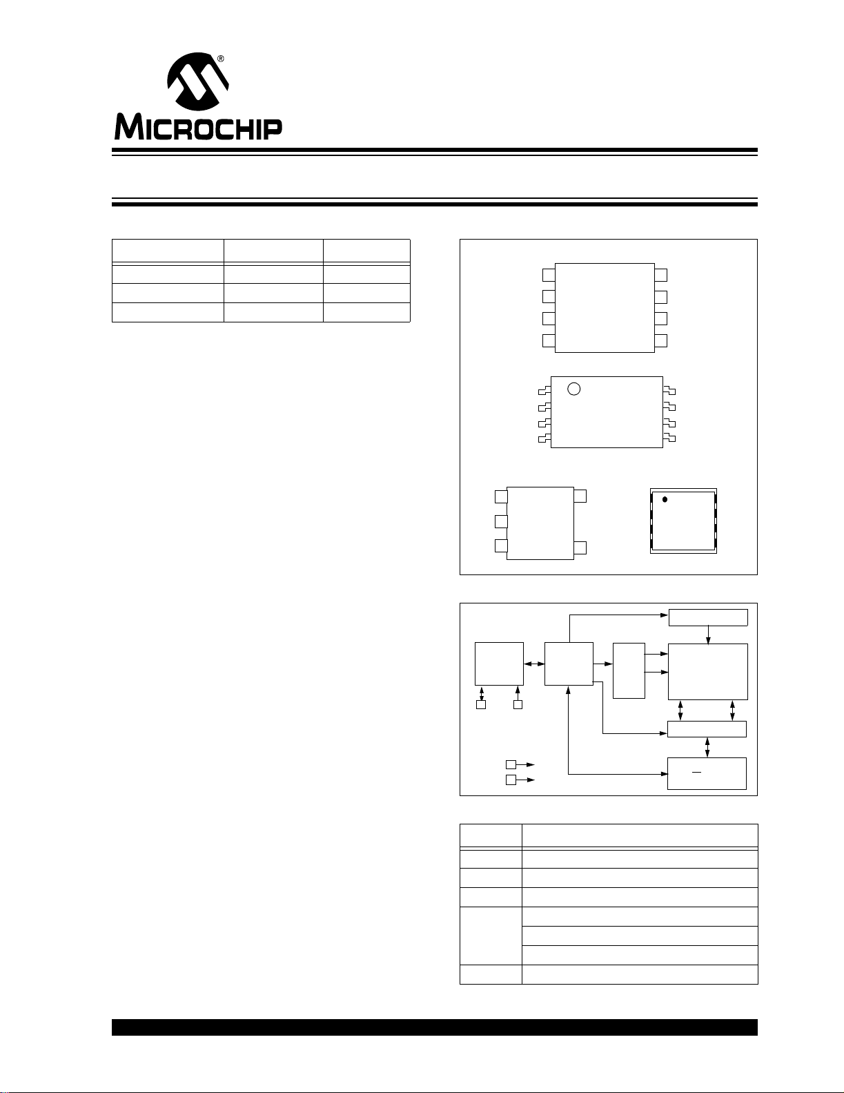
Device Selection Table
Device VCC Range Temp Range
24AA00 1.8-5.5 C,I
24LC00 2.5-5.5 C,I
24C00 4.5-5.5 C,I,E
Features:
• Low-power CMOS technology:
- 500 μA typical ac tive current
- 250 nA typical standby current
• Organized as 16 bytes x 8 bits
• 2-wire serial interface bus, I
• 100 kHz (1.8V) and 400 kHz (5V) compatibility
• Self-timed write cycle (including auto-erase)
• 4 ms maximum byte write cycle time
• 1,000,000 erase/write cycles
• ESD protection > 4 kV
• Data retention > 200 years
• 8L PDIP, SOIC, TSSOP, DFN and 5L SOT-23
packages
• Pb-free finish available
• Temperature ranges available:
- Commercial (C): 0°Cto+70°C
- Industrial (I): -40°Cto+85°C
- Automotive (E): -40°C to +125°C
2
C™ compatible
Package Types
8-PIN PDIP/SOIC
NC
NC
NC
Vss
8-PIN TSSOP
1
NC
2
NC
3
NC
SS
4
V
5-PIN SOT-23
SCL
15
SS
V
2
SDA
3
Block Diagram
I/O
Control
Logic
Memory
Control
1
2
3
4
4
Logic
VCC
NC
V
XDEC
NC
NC
NC
CC
V
8
7
NC
6
SCL
5
SDA
8
VCC
7
NC
6
SCL
5
SDA
DFN
1
2
3
SS
4
HV Generator
8
7
6
5
EEPROM
Array
CC
V
NC
SCL
SDA
Description:
SCL
The Microchip Technology Inc. 24AA00/24LC00/
24C00 (24XX00*) is a 128-bit Electrically Erasable
PROM memory organized as 16 x 8 with a 2-wire
serial interface. Low-voltage design permits operation
down to 1.8 volts for th e 24AA00 version, an d every
version maintains a maximum standby current of only
1 μA and typical active current of only 500 μA. This
device was designed for where a small amount of
EEPROM is needed for the storage of calibration
values, ID numbers or manufacturing information, etc.
The 24XX00 is available in 8-pin PDIP, 8-pin SOIC
(150 mil), 8-pin TSS OP, 8-pin 2x3 DFN and the 5-pin
SOT-23 packages.
I2C is a trademark of Philips Corporation.
*24XX00 is used in this document as a generic part number for
the 24AA00/24LC00/24C00 devices.
© 2005 Microchip Technology Inc. DS21178E-page 1
SDA
VCC
VSS
Pin Function Table
Name Function
V
SS Ground
SDA Serial Data
SCL Serial Clock
CC +1.8V to 5.5V (24AA00)
V
+2.5V to 5.5V (24LC00)
+4.5V to 5.5V (24C00)
NC No Internal Connection
YDEC
Sense AMP
R/W
Control
24AA00/24LC00/24C00
1.0 ELECTRICAL CHARACTERISTICS
Absolute Maximum Ratings
VCC.............................................................................................................................................................................6.5V
All inputs and outputs w.r.t. V
Storage temperature ...............................................................................................................................-65°C to +150°C
Ambient temperature with power applied................................................................................................-65°C to +125°C
ESD protection on all pins..........................................................................................................................................4 kV
† NOTICE: Stresses above those listed under “Absolute Maximum Ratings” may cause permanent damage to
the device. This is a stress rating only and functional operation of the device at those or any other conditions
above those indica ted in the opera tional li stings of this sp ecification is not i mplied. Ex posure to maximum rating
conditions for extended periods may affect device reliability.
(†)
SS ......................................................................................................... -0.6V to VCC +1.0V
TABLE 1-1: DC CHARACTERISTICS
All Parameters apply across the
recommended operating ranges unless
otherwise noted
Parameter Symbol Min. Max. Units Conditions
SCL and SDA pins:
High-level input voltage
Low-level input voltage VIL —0.3 VCC V (Note)
Hysteresis of Schmitt Trigger
inputs
Low-level output voltage V
Input leakage current I
Output leakage current ILO —±1μAVOUT = VCC or VSS
Pin capacitance (all inputs/outputs) CIN,
Operating current ICC Write — 2 mA VCC = 5.5V, SCL = 400 kHz
Standby current I
Note: This parameter is periodically sampled and not 100% tested.
Commercial (C): TA = 0°C to +70°C, VCC = 1.8V to 5.5V
Industrial (I): T
Automotive (E) T
VIH 0.7 VCC —V(Note)
VHYS .05 VCC —VVCC ≥ 2.5V (Note)
OL —0.4VIOL = 3.0 mA, VCC = 4.5V
LI —±1μAVIN = VCC or VSS
C
OUT
ICC Read — 1 mA VCC = 5.5V, SCL = 400 kHz
CCS —1μAVCC = 5.5V, SDA = SCL = VCC
A = -40°C to +85°C, VCC = 1.8V to 5.5V
A = -40°C to +125°C, VCC = 4.5V to 5.5V
OL = 2.1 mA, VCC = 2.5V
I
—10pFVCC = 5.0V (Note)
T
A = 25°C, FCLK = 1 MHz
FIGURE 1-1: BUS TIMING DATA
TF
SCL
SDA
IN
SDA
OUT
DS21178E-page 2 © 2005 Microchip Technology Inc.
TSU:STA
TSP
HD:STA
T
TLOW
THIGH
THD:DAT
TAA
TSU:DAT
TR
TSU:STO
TBUF

TABLE 1-2: AC CHARACTERISTICS
24AA00/24LC00/24C00
All Parameters apply across all
recommended operating ranges
unless otherwise noted
Commercial (C): T
Industrial (I): T
Automotive (E): T
A = 0°C to +70°C, VCC = 1.8V to 5.5V
A = -40°C to +85°C, VCC = 1.8V to 5.5V
A = -40°C to +125°C, VCC = 4.5V to 5.5V
Parameter Symbol Min Max Units Conditions
Clock frequency F
Clock high time THIGH 4000
Clock low time TLOW 4700
SDA and SCL rise time
(Note 1)
CLK —
—
—
4000
600
4700
1300
TR —
—
—
100
100
400
—
—
—
—
—
—
1000
1000
300
kHz 4.5V ≤ Vcc ≤ 5.5V (E Temp range)
1.8V ≤ Vcc ≤ 4.5V
4.5V ≤ Vcc ≤ 5.5V
ns 4.5V ≤ Vcc ≤ 5.5V (E Temp range)
1.8V ≤ Vcc ≤ 4.5V
4.5V ≤ Vcc ≤ 5.5V
ns 4.5V ≤ Vcc ≤ 5.5V (E Temp range)
1.8V ≤ Vcc ≤ 4.5V
4.5V ≤ Vcc ≤ 5.5V
ns 4.5V ≤ Vcc ≤ 5.5V (E Temp range)
1.8V ≤ Vcc ≤ 4.5V
4.5V ≤ Vcc ≤ 5.5V
SDA and SCL fall time TF —300ns(Note 1)
Start condition hold time THD:STA 4000
4000
600
Start condition setup time TSU:STA 4700
4700
600
—
—
—
—
—
—
ns 4.5V ≤ Vcc ≤ 5.5V (E Temp range)
1.8V ≤ Vcc ≤ 4.5V
4.5V ≤ Vcc ≤ 5.5V
ns 4.5V ≤ Vcc ≤ 5.5V (E Temp range)
1.8V ≤ Vcc ≤ 4.5V
4.5V ≤ Vcc ≤ 5.5V
Data input hold time THD:DAT 0—ns(Note 2)
Data input setup time T
Stop condition setup time T
Output valid from clock
(Note 2)
Bus free time: T i me the b us must
be free before a new transmission can start
Output fall time from V
IH
minimum to VIL maximum
Input filter spike suppression
SU:DAT 250
250
100
SU:STO 4000
4000
600
AA —
T
—
—
BUF 4700
T
4700
1300
T
OF 20+0.1
—
—
—
—
—
—
3500
3500
900
—
—
—
ns 4.5V ≤ Vcc ≤ 5.5V (E Temp range)
1.8V ≤ Vcc ≤ 4.5V
4.5V ≤ Vcc ≤ 5.5V
ns 4.5V ≤ Vcc ≤ 5.5V (E Temp range)
1.8V ≤ Vcc ≤ 4.5V
4.5V ≤ Vcc ≤ 5.5V
ns 4.5V ≤ Vcc ≤ 5.5V (E Temp range)
1.8V ≤ Vcc ≤ 4.5V
4.5V ≤ Vcc ≤ 5.5V
ns 4.5V ≤ Vcc ≤ 5.5V (E Temp range)
1.8V ≤ Vcc ≤ 4.5V
4.5V ≤ Vcc ≤ 5.5V
250 ns (Note 1), CB ≤ 100 pF
CB
SP —50ns(Notes 1, 3)
T
(SDA and SCL pins)
Write cycle time T
WC —4ms
Endurance 1M — cycles (Note 4)
Note 1: Not 100% tested. C
B = total capacitance of one bus line in pF.
2: As a transmitter, the device must provide an internal minimum delay time to bridge the undefined region
(minimum 300 ns) of the falling edge of SCL to avoid unintended generation of Start or Stop conditions.
3: The combine d T
SP and VHYS specifications are due to new Schmit t Trigger inputs w h ic h p rov id e i mp rov ed
noise spike suppression. This eliminates the need for a TI specification for standard operation.
4: This parameter is not tested but ensured by c haracterization. For endurance estimates in a speci fic
application, please consult the Total Endurance™ Model which can be obtained at www.microchip.com.
© 2005 Microchip Technology Inc. DS21178E-page 3

24AA00/24LC00/24C00
2.0 PIN DESCRIPTIONS
2.1 SDA Serial Data
This is a bidirectional pin used to transfer addresses
and data into and data out of the device. It is an open
drain terminal, therefore the SDA bus requires a pull-up
resistor to V
400 kHz).
For normal data t ransfer SDA is all owed to change only
during SCL low. Changes during SCL high are
reserved for indicating the Start and Stop conditions.
CC (typical 10 kΩ for 100 kHz, 2 kΩ for
2.2 SCL Serial Clock
This input is u sed t o sy nchron ize the d ata trans fer fro m
and to the device.
2.3 Noise Protection
The SCL and SDA inputs have Schmitt Trigger and
filter circuits which suppress noise spikes to assure
proper device operation even on a noisy bus.
3.0 FUNCTIONAL DESCRIPTION
The 24XX00 supports a bidirectional 2-wire bus and
data transmission protocol. A device that sends data
onto the bus is defined as a transmitter, and a device
receiving data as a receiver. The bus has to be
controlled by a master device which generates the
Serial Clock (SCL), controls the bus access, and
generates the Start and Stop conditions, while the
24XX00 works as slave. Both master and slave can
operate as transmitter or receiver, but the master
device determines which mode is activated.
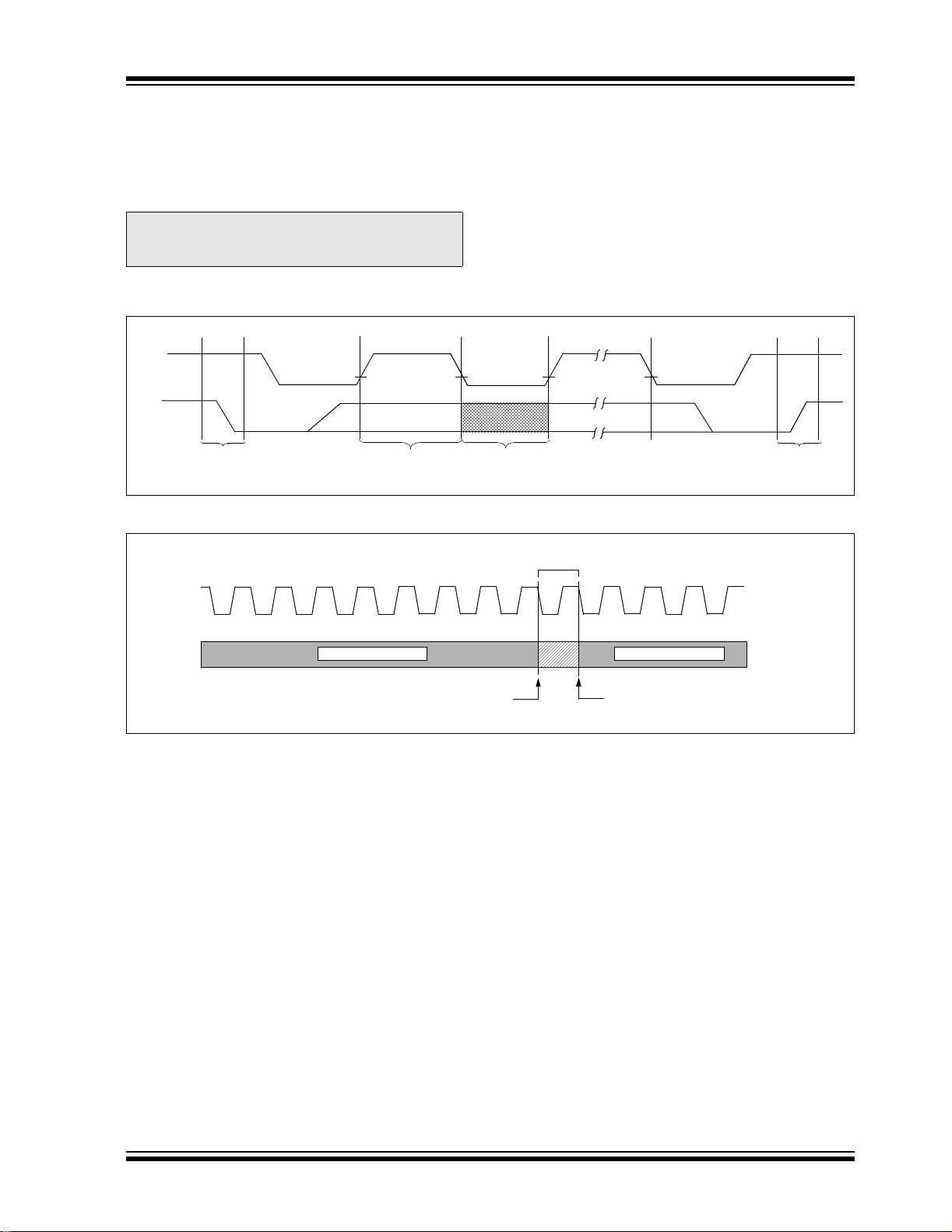
4.0 BUS CHARACTERISTICS
The following bus protocol has been defined:
• Data transfer may be initiated only when the bus
is not busy.
• During data transfer, the data line must remain
stable wheneve r the cl ock lin e is high . Changes i n
the data line while the clock line is high will be
interpreted as a Start or Stop condition.
Accordingly, the following bus conditions have been
defined (Figure 4-1).
4.1 Bus Not Busy (A)
Both data and clock lines remain high.
4.2 Start Data Transfer (B)
A high-to- lo w t ran si t i on of t h e SD A l in e whi l e t h e c lo ck
(SCL) is high determines a Start condition. All
commands must be preceded by a Start condition.
4.3 Stop Data Transfer (C)
A low-to-high transition of the SDA line while the clock
(SCL) is high determines a Stop condition. All
operations must be ended with a Stop condition.
4.4 Data Valid (D)
The state of the data line represents valid data when,
after a Start condition, the data line is stable for the
duration of the high period of the clock signal.
The data on the line must be changed during the low
period of the clock signal. There is one bit of data per
clock pulse.
Each data transfer is initiated with a S tart condition and
terminated with a Stop condition. The number of the
data bytes transferred between the Start and Stop
conditions is determined by the master device and is
theoretically unlimited.
DS21178E-page 4 © 2005 Microchip Technology Inc.
24AA00/24LC00/24C00
4.5 Acknowledge
Each receiving device, when addressed, is obliged to
generate an acknowledge after the reception of each
byte. The master device must generate an extra clock
pulse which is associated with this Acknowledge bit.
Note: The 24XX00 does not generate any
Acknowledge bits if an internal programming cycle is in progress.
The device that acknowledges has to pull down the
SDA line during the Acknowl edge cloc k pulse in s uch a
way that the SDA line is stable low during the high
period of the acknowledge related clock pulse. Of
course, setup and hold times must be taken into
account. A master must signal an end of data to the
slave by not gene rati ng an Ac kno w led ge bi t o n th e last
byte that has been clocked out of the slave. In this
case, the slave must leave the data line high to enable
the master to generate the Stop condition (Figur e 4-2).
FIGURE 4-1: DATA TRANSFER SEQUENCE ON THE SERIAL BUS
SCL
SDA
(A)
Condition
(B)
Start
(C)
Address or
Acknowledge
Valid
Data
Allowed
to Change
(D)
FIGURE 4-2: ACKNOWLEDGE TIMING
Acknowledge
Bit
Stop
Condition
(A)(C)
SCL
SDA
Data from transmitter
Transmitter must release the SDA line at this point
allowing the Receiver to pull the SDA line low to
acknowledge the previous eight bits of data.
987654321 123
Data from transmitter
Receiver must release the SDA line at this point
so the Transmitter can continue sending data.
© 2005 Microchip Technology Inc. DS21178E-page 5
24AA00/24LC00/24C00
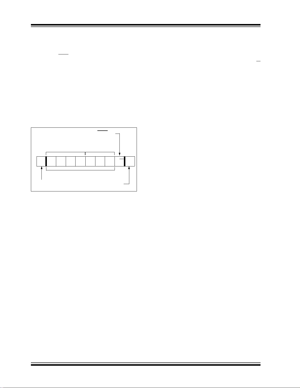
5.0 DEVICE ADDRESSING
After generating a Start condition, the bus master
transmits a control byte consisting of a slave address
and a Read/Write bit that indicates what type of
operation is to be perfo rmed. The sl ave addres s for the
24XX00 consists of a 4-bit device code ‘1010’ followed
by three “don’t care” bits.
The last bit of the control byte determine s the operation
to be performed. When set to a o ne a read operati on is
selected, and when set to a zero a write operation is
selected (Figure 5-1). The 24XX00 monitors the bus for
its corresponding slave address all the time. It
generates an Ackn owledge bit if the sla ve addres s was
true and it is not in a programming mode.
FIGURE 5-1: CONTROL BYTE FORMAT
Bit
Bits
Start Bit
Read/Write
Device Select
Bits
1010xxxSACKR/W
Slave Address
Don’t Care
Acknowledge Bit
6.0 WRITE OPERATIONS
6.1 Byte Write
Following the Start signal from the master, the device
code (4 bits), the “don’t care” bits (3 bits), and the R/W
bit (which is a logic low) are placed onto the bus by the
master transmitter. This indicates to the addressed
slave receiver that a byte with a word address will
follow after it has generated an Acknowl edge bit durin g
the ninth clock cycl e. Therefore, the next byte t ransmitted by the master is the word address and will be
written into the Address Pointer of the 24XX00. Only
the lower four address bit s are us ed by t he device , and
the upper four bits are “don’t cares.” The 24XX00 will
acknowledge the address byte and the master device
will then transmit the data word to be written into the
addressed memory location. The 24XX00 acknowledges again and the master generates a Stop
condition. This initiates the internal write cycle, and
during this time the 24XX00 will not ge nerate Ack now ledge signals (Figure7-2). After a by te Wr ite co mmand,
the internal address counter will not be incremented
and will point to the s ame address lo cation that was jus t
written. If a Stop bit is transmitted to the device at any
point in the Write comman d sequenc e before the e ntire
sequence is complete, then the command will abort
and no data will be written. If more than 8 data bits are
transmitted before the Stop bit is sent, then the device
will clear the previously loaded byte and begin loading
the data buffer again. If more than one data byte is
transmitted to the device and a Stop bit is sent before a
full eight data bits have been transmitted, then the
Write command will abort and no data will be written.
The 24XX00 employs a V
which disables the internal erase/write logic if the V
is below 1.5V (24AA00 and 24LC00) or 3.8V (24C00)
at nominal conditions.
CC threshold detector circuit
CC
DS21178E-page 6 © 2005 Microchip Technology Inc.
24AA00/24LC00/24C00
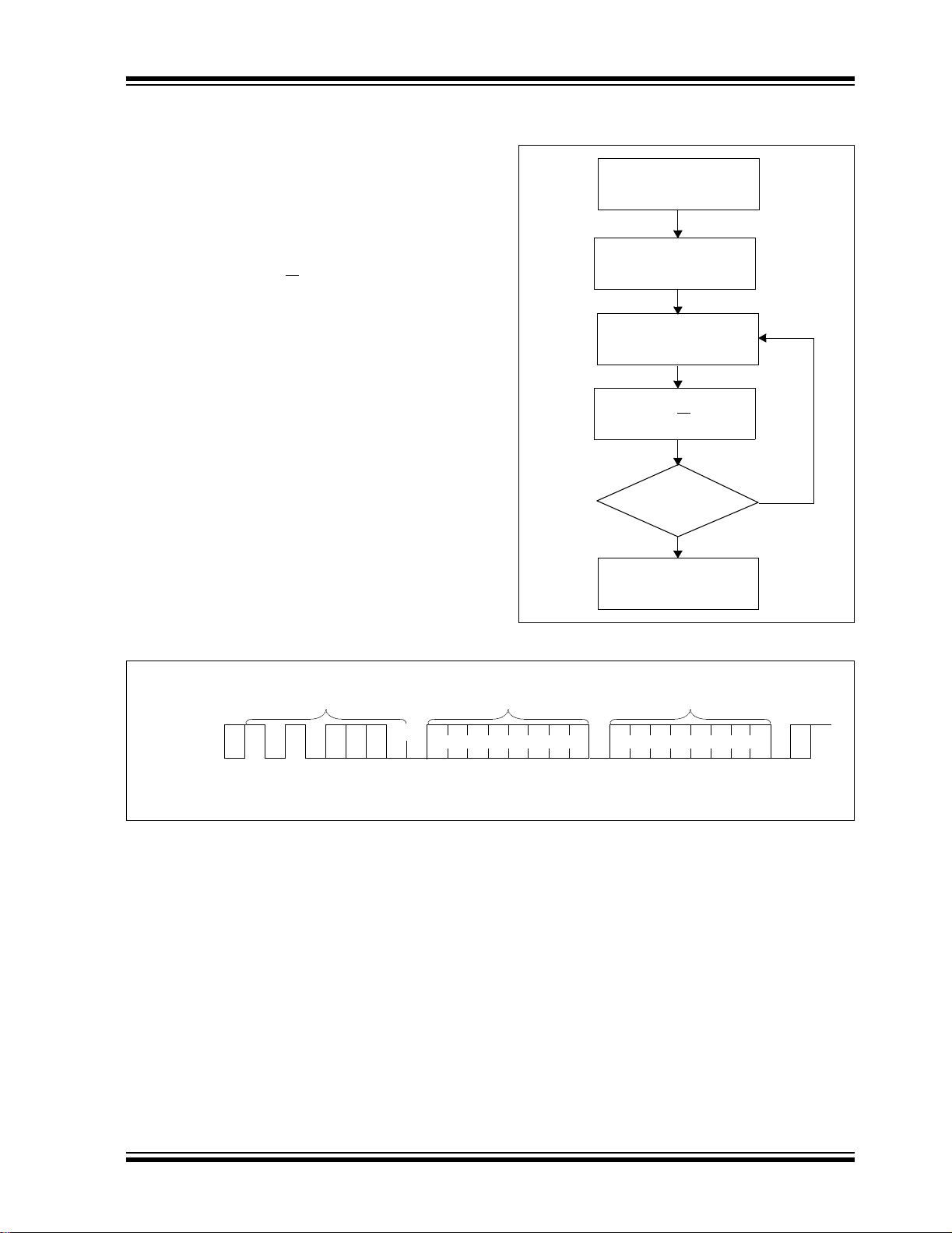
7.0 ACKNOWLEDGE POLLING
Since the device will not acknowledge during a write
cycle, this can be used to determine when the cycle is
complete (this feature can be used to maximize bus
throughput). Once the Stop condition for a Write
command has been issu ed from the mas ter , the device
initiates the internally timed write cycle. ACK polling
can be initiated immediately. This involves the master
sending a Start condition followed by the control byte
for a Write command (R/W
busy with the write cycle, then no ACK will be returned.
If no ACK is returne d, then th e S t art bit and control byte
must be re-sent. If the cycle is complete, then the
device will return the ACK and the master can then
proceed with the next Read or Write command. See
Figure 7-1 for flow diagram.
= 0). If the device is still
FIGURE 7-1: ACKNOWLEDGE
POLLING FLOW
Send
Write Command
Send Stop
Condition to
Initiate Write Cycle
Send Start
Send Control Byte
with R/W = 0
Did Device
Acknowledge
(ACK = 0)?
Yes
No
FIGURE 7-2: BYTE WRITE
S
BUS ACTIVITY
MASTER
SDA LINE
BUS ACTIVITY
x = “don’t care” bit
T
A
R
T
S
10 x10 xxx
Control
Byte
Next
Operation
Word
Address
A
C
K
xxx
A
C
K
0
Data
S
T
O
P
P
A
C
K
© 2005 Microchip Technology Inc. DS21178E-page 7

24AA00/24LC00/24C00
8.0 READ OPERATIONS
Read operations are initiated in the same way as write
operations with the exception that the R/W
slave address is set to one. The re are three ba sic types
of read operations: current add ress read , rand om rea d
and sequential read.
8.1 Current Address Read
The 24XX00 contains an address counter that maintains the address of the last word accessed, internally
incremented by one. Therefore, if the previous read
access was to address n, the next current address read
operation would acc ess dat a f rom add ress n + 1. Upon
receipt of the slave a ddress with the R/W
the device issues an acknowledge and transmits the
eight-bit data word. The master will not acknowledge
the transfer , but does generate a S top con dition and the
device discontinues transmission (Figure8-1).
8.2 Random Read
Random read operations allow the master to access
any memory location in a random manner. To perform
this type of read operatio n, fi rst the word address must
be set. This is d one by sending the word a ddress to the
device as part of a write operation.
bit of the
bit set to one,
After the word address is sent, the master generates a
Start condition following the acknowledge. This terminates the write operation, but not before the internal
Address Pointer is set. Then the master issues the
control byte again, but with the R/W
bit set to a one.
The 24XX00 will then i ssue an ack nowledge a nd transmits the eight bit data word. The master will not
acknowledge the transfer, but does generate a Stop
condition and the device discontinues transmission
(Figure 8-2). After this command, the internal address
counter will point to the address location following the
one that was just read.
8.3 Sequential Read
Sequential reads are initiated in the same way as a
random read except that after the device transmits the
first data byte, the master issues an acknowledge as
opposed to a Stop condition in a random read. This
directs the device to transmit the next sequentially
addressed 8-bit word (Figure 8-3).
To provide se quential reads the 2 4XX00 contains an
internal Address Pointer which is incremented by one
at the complet ion o f e ach r ead o peratio n. Thi s Add ress
Pointer allows the entire memory contents to be serially
read during one operation.
FIGURE 8-1: CURRENT ADDRESS READ
S
BUS ACTIVITY
MASTER
SDA LINE
BUS ACTIVITY
x = “don’t care” bit
T
A
R
T
1100xxx1
Control
Byte
S
Data
A
C
K
T
O
P
PS
N
O
A
C
K
DS21178E-page 8 © 2005 Microchip Technology Inc.

FIGURE 8-2: RANDOM READ
S
BUS ACTIVITY
MASTER
SDA LINE
T
Control
A
R
T
Byte
S 1100xxx0
BUS ACTIVITY
x = “don’t care” bit
FIGURE 8-3: SEQUENTIAL READ
BUS ACTIVITY
MASTER
SDA LINE
BUS ACTIVITY
Control
Byte
Data n Data n + 1 Data n + 2 Data n + x
A
C
K
xxxx
A
C
K
A
C
K
Word
Address(n)
24AA00/24LC00/24C00
S
T
Control
A
R
T
Byte
S 110 0xxx 1
A
C
K
A
C
K
Data (n)
A
C
K
A
C
K
S
T
O
P
P
N
O
A
C
K
S
T
O
P
P
N
O
A
C
K
© 2005 Microchip Technology Inc. DS21178E-page 9
24AA00/24LC00/24C00
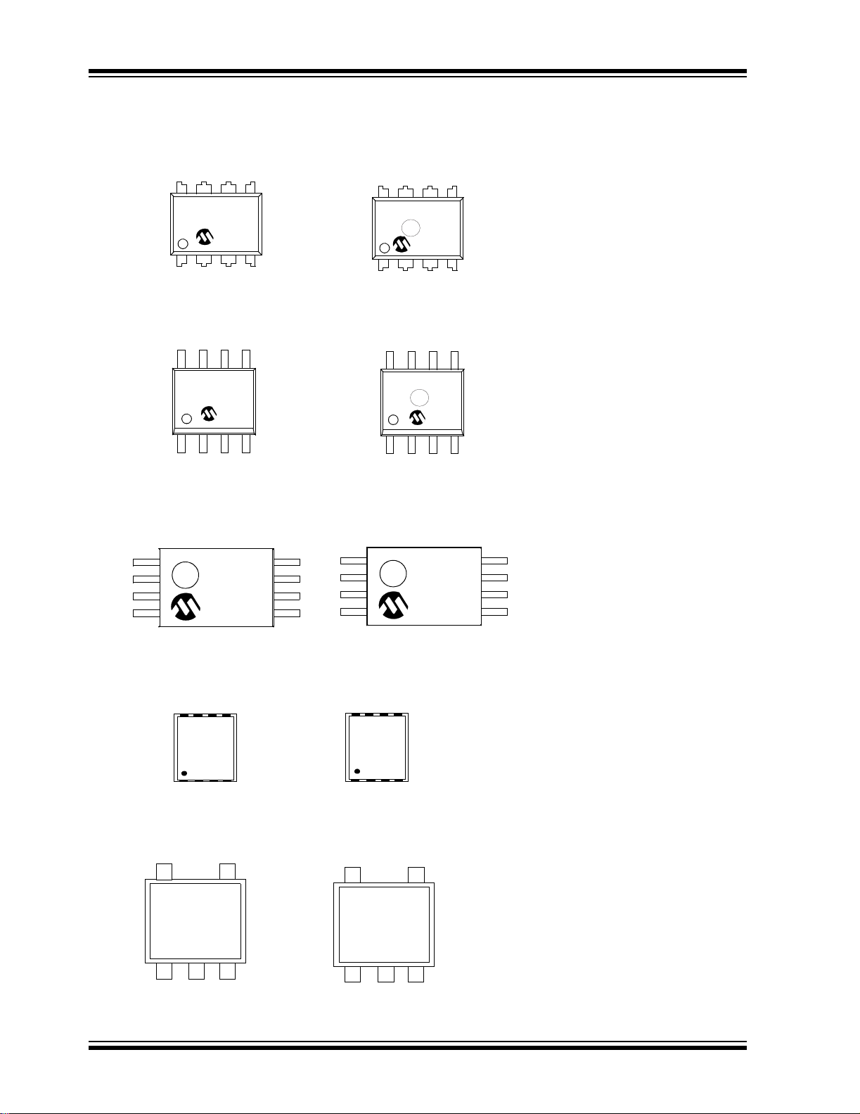
9.0 PACKAGING INFORMATION
9.1 Package Marking Information
8-Lead PDIP (300 mil)
XXXXXXXX
T/XXXNNN
YYWW
8-Lead SOIC (150 mil)
XXXXXXXT
XXXXYYWW
NNN
8-Lead TSSOP
XXXX
TYWW
NNN
Example:
24LC00
I/P 13F
Example:
Example:
3
e
0527
24LC00I
3
e
SN 0527
13F
4L00
I527
13F
8-Lead 2x3 DFN
XXX
YWW
NN
5-Lead SOT-23
XXNN
DS21178E-page 10 © 2005 Microchip Technology Inc.
Example:
204
527
13
Example:
M03F

24AA00/24LC00/24C00
l
1st Line Marking Codes
Part Number
24AA00 4A00 A0NN B0NN — 201 —
24LC00 4L00 L0NN M0NN — 204 —
24C00 4C00 C0NN D0NN E0NN 207 208
Note: NN = Alphanumeric traceability code
Legend: XX...X Part number or part number code
Note: For very small packages with no room for the Pb-free JEDEC designator
Note: In the event the full Microchip part num ber can not be ma rked on one line , it wil
TSSOP
T Temperature (I, E)
Y Year code (last digit of calendar year)
YY Year code (last 2 digits of calendar year)
WW Week code (w eek of January 1 is week ‘01’)
NNN Alphanumeric traceability code (2 characters for small packages)
Pb-free JEDEC designator for Matte Tin (Sn)
3
e
, the marking will only appear on the outer carton or reel label.
3
e
be carried over to the next line, thus limiting the number of available
characters for customer-specific information.
C Temp. I Temp. E Temp. I Temp. E Temp.
SOT-23 DFN
Note: Please visit www.microchip.com/Pbfree for the latest information on Pb-free conversion.
*Standard OTP marking consists of Microchip part number, year code, week code, and traceability code.
© 2005 Microchip Technology Inc. DS21178E-page 11

24AA00/24LC00/24C00
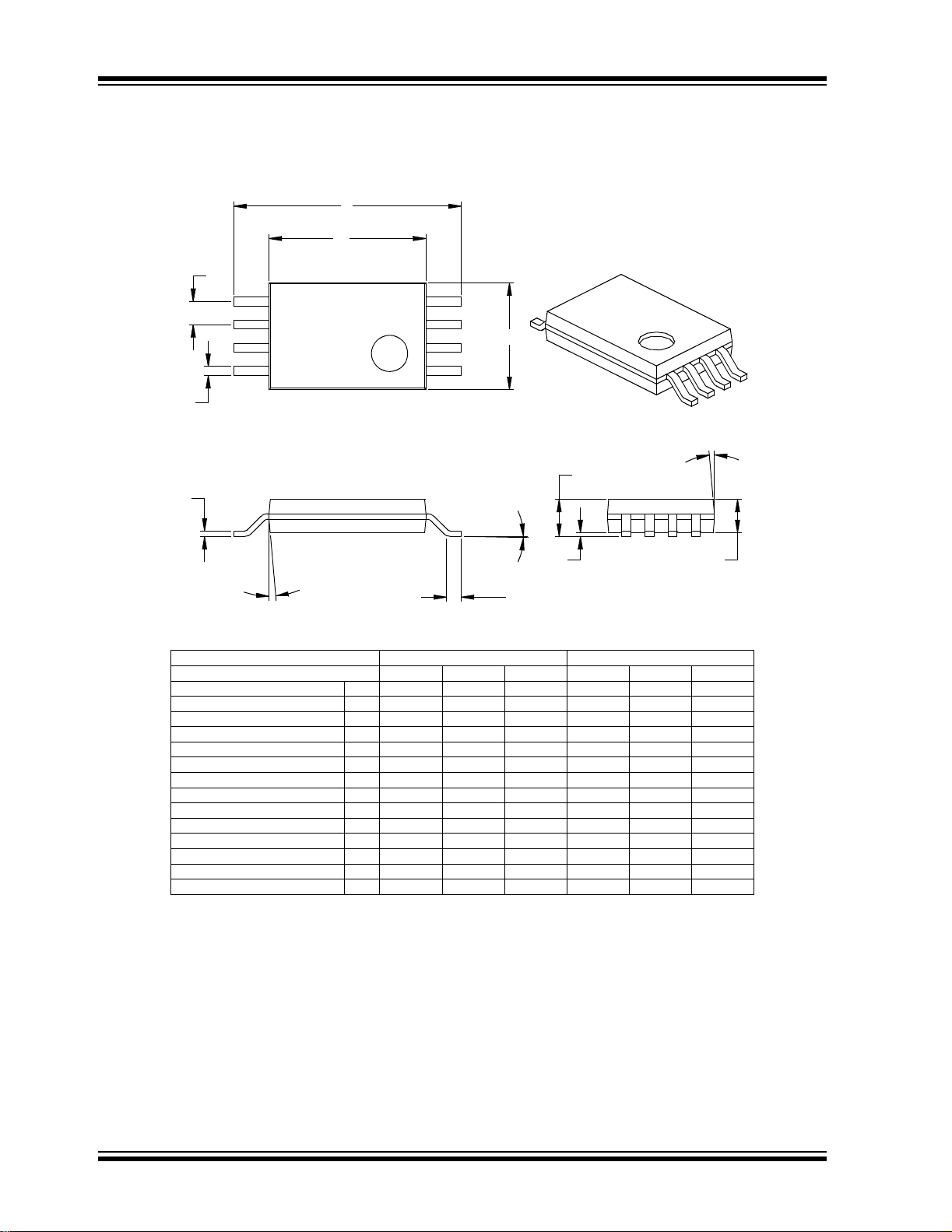
8-Lead Plastic Dual In-line (P) – 300 mil (PDIP)
E1
D
2
n
E
β
eB
Number of Pins
Pitch
Top to Seating Plane A .140 .155 .170 3.56 3.94 4.32
Molded Package Thickness A2 .115 .130 .145 2.92 3.30 3.68
Base to Seating Plane A1 .015 0.38
Shoulder to Shoulder Width E .300 .313 .325 7.62 7.94 8.26
Molded Package Width E1 .240 .250 .260 6.10 6.35 6.60
Overall Length D .360 .373 .385 9.14 9.46 9.78
Tip to Seating Plane L .125 .130 .135 3.18 3.30 3.43
Lead Thickness
Upper Lead Width B1 .045 .058 .070 1.14 1.46 1.78
Lower Lead Width B .014 .018 .022 0.36 0.46 0.56
Overall Row Spacing § eB .310 .370 .430 7.87 9.40 10.92
Mold Draft Angle Top
Mold Draft Angle Bottom
* Controlling Parameter
§ Significant Characteristic
Notes:
Dimensions D and E1 do not include mold flash or protrusions. Mold flash or protrusions shall not exceed
.010” (0.254mm) per side.
JEDEC Equivalent: MS-001
Drawing No. C04-018
Dimension Limits MIN NOM MAX MIN NOM MAX
1
α
A
c
Units INCHES* MILLIMETERS
n
p
c
α
β
.008 .012 .015 0.20 0.29 0.38
A1
B1
B
88
.100 2.54
51015 51015
51015 51015
A2
L
p
DS21178E-page 12 © 2005 Microchip Technology Inc.

24AA00/24LC00/24C00
8-Lead Plastic Small Outline (SN) – Narrow, 150 mil (SOIC)
E
E1
p
D
2
B
Number of Pins
Pitch
Standoff §
Foot Angle
Lead Thickness
Mold Draft Angle Top
Mold Draft Angle Bottom
* Controlling Parameter
§ Significant Characteristic
Notes:
Dimensions D and E1 do not include mold flash or protrusions. Mold flash or protrusions shall not exceed
.010” (0.254mm) per side.
JEDEC Equivalent: MS-012
Drawing No. C04-057
n
45°
c
β
n
p
A1
φ
c
α
β
1
h
A
φ
L
048048
A1
MILLIMETERSINCHES*Units
α
A2
MAXNOMMINMAXNOMMINDimension Limits
88
1.27.050
1.751.551.35.069.061.053AOverall Height
1.551.421.32.061.056.052A2Molded Package Thickness
0.250.180.10.010.007.004
6.206.025.79.244.237.228EOverall Width
3.993.913.71.157.154.146E1Molded Package Width
5.004.904.80.197.193.189DOverall Length
0.510.380.25.020.015.010hChamfer Distance
0.760.620.48.030.025.019LFoot Length
0.250.230.20.010.009.008
0.510.420.33.020.017.013BLead Width
1512015120
1512015120
© 2005 Microchip Technology Inc. DS21178E-page 13
24AA00/24LC00/24C00
8-Lead Plastic Thin Shrink Small Outline (ST) – 4.4 mm (TSSOP)
E
E1
p
D
2
n
B
1
A
c
A1
φ
β
Units
A1
n
p
φ
c
α
β
048048
Number of Pins
Pitch
Standoff §
Foot Angle
Lead Thickne ss
Mold Draft Angle Top
Mold Draft Angle Bottom
* Controlling Parameter
§ Significant Characteristic
Notes:
Dimensions D and E1 do not include mold flash or protrusions. Mold flash or protrusions shall not exceed
.005” (0.127mm) per side.
JEDEC Equivalent: MO-153
Drawing No. C04-086
L
MILLIMETERS*INCHES
0.65.026
α
A2
MAXNOMMINMAXNOMMINDimension Limits
88
1.10.043AOverall Height
0.950.900.85.037.035.033A2Molded Package Thickness
0.150.100.05.006.004.002
6.506.386.25.256.251.246EOverall Width
4.504.404.30.177.173.169E1Molded Package Width
3.103.002.90.122.1 18.114DMolded Package Length
0.700.600.50.028.024.020LFoot Length
0.200.150.09.008.006.004
0.300.250.19.012.010.007BLead Wi dth
10501050
10501050
DS21178E-page 14 © 2005 Microchip Technology Inc.
24AA00/24LC00/24C00
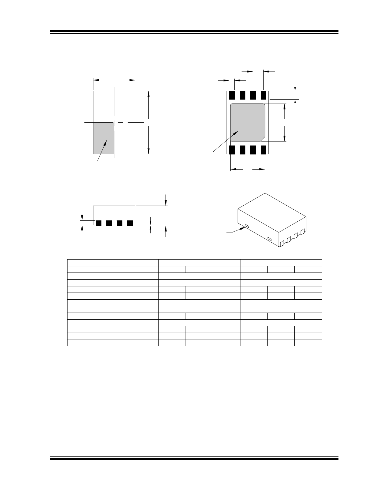
8-Lead Plastic Dual Flat No Lead Package (MC) 2x3x0.9 mm Body (DFN) – Saw Singulated
p
D
b
n
L
PIN 1
ID INDEX
AREA
(NOTE 2)
TOP VIEW
A3
Dimension Limits
Number of Pins
Pitch
Overall Height
Standoff
Contact Thickness
Overall Length
3)
(Note
(Note
3)
Exposed Pad Length
Overall Width
Exposed Pad Width
Contact Width
Contact Length
*Controlling Parameter
Notes:
Package may have one or more exposed tie bars at ends.1.
Pin 1 visual index feature may vary, but must be located within the hatched area.2.
3.
Exposed pad dimensions vary with paddle size.
4. JEDEC equivalent: MO-229
Drawing No. C04-123
E
Units
n
p
A
A1
A3
D
D2
E
E2
b
L
A1
EXPOSED
A
MIN
.031
.000 .001
.055
.047
.008
.012
METAL
PAD
21
D2
BOTTOM VIEW
EXPOSED
TIE BAR
(NOTE 1)
INCHES
NOM
8
.020 BSC
.039
.002
.008 REF.
.079 BSC
-- --
.118 BSC
-- -.010
.016
.064
.071
.012
.020
MINMAX NOM
0.80
0.00
1.39
1.20
0.20
0.30
E2
MILLIMETERS*
8
0.50 BSC
0.90.035
0.02
0.20 REF.
2.00 BSC
3.00 BSC
0.25
0.40
Revised 05/24/04
MAX
1.00
0.05
1.62
1.80
0.30
0.50
© 2005 Microchip Technology Inc. DS21178E-page 15

24AA00/24LC00/24C00
5-Lead Plastic Small Outline Transistor (OT) (SOT-23)
E
E1
p
B
p1
D
n
c
β
Number of Pins
Pitch
Outside lead pitch (basic)
Foot Angle
Lead Thickne ss
Mold Draft Angle Top
Mold Draft Angle Bottom
* Controlling Parameter
§ Significant Characteristic
Notes:
Dimensions D and E1 do not include mold flash or protrusions. Mold flash or protrusions shall not exceed
.010” (0.254mm) per side.
JEDEC Equivalent: MO-178
Drawing No. C04-091
1
A
φ
L
n
p
p1
φ
c
α
β
.038
A1
MILLIMETERSINCHES*Units
0.95
1.90.075
α
A2
MAXNOMMINMAXNOMMINDimension Limits
55
1.451.180.90.057.046.035AOverall Height
1.301.100.90.051.043.035A2Molded Package Thickness
0.150.080.00.006.003.000A1Standoff §
3.002.802.60.118.110.102EOverall Width
1.751.631.50.069.064.059E1Molded Package Width
3.102.952.80.122.116.110DOverall Length
0.550.450.35.022.018.014LFoot Length
10501050
0.200.150.09.008.006.004
0.500.430.35.020.017.014BLead Width
10501050
10501050
DS21178E-page 16 © 2005 Microchip Technology Inc.

APPENDIX A: REVISION HISTORY
Revision E
Added DFN package.
24AA00/24LC00/24C00
© 2005 Microchip Technology Inc. DS21178E-page 17

24AA00/24LC00/24C00
NOTES:
DS21178E-page 18 © 2005 Microchip Technology Inc.

24AA00/24LC00/24C00
THE MICROCHIP WEB SITE
Microchip provides onlin e support v ia our W WW site at
www.m ic roc hi p.c om . Thi s web si te i s us ed as a m ean s
to make files and information easily available to
customers. Accessible by using your favorite Internet
browser, the web site contains the following
information:
• Product Support – Data sheets and errata,
application notes and sample programs, design
resources, user’s guides and hardware support
documents, lat est softwa re releases and archived
software
• General Technical Support – Frequently Asked
Questions (FAQ), technical support requests,
online discussion groups, Microchip consultan t
program member listing
• Business of Microchip – Product selector and
ordering guides, latest Microchip press releases,
listing of s eminars and events, listings of
Microchip sales offices, distributors and factory
representatives
CUSTOMER CHANGE NOTIFICATION SERVICE
Microchip’s customer notification service helps keep
customers current on Microchip products. Subscribers
will receive e-mail notification whenever there are
changes, updates, revisions or errata related to a
specified produ ct family or develo pment tool of inte rest.
To register, access the Microchip web site at
www.microchip.com, click on Customer Change
Notification and follow the registration instructions.
CUSTOMER SUPPORT
Users of Microchip products can receive assistance
through several channels:
• Distributor or Representative
• Local Sal es Office
• Field Application Engineer (FAE)
• Technical Support
• Development Systems Information Line
Customers should contact their distributor,
representative or field application engineer (FAE) for
support. Local sales offices are also available to help
customers. A listing of sales offices and locations is
included in the back of this document.
T echnic al support is avail able throug h the web si te
at: http://support.microchip.com
In addition, there is a Development Systems
Information Line which lists the latest versions of
Microchip’s development systems software products.
This line also provides information on how customers
can receive currently available upgrade kits.
The Development Systems Information Line
numbers ar e:
1-800-755-2345 – United States and most of Canada
1-480-792-7302 – Other International Locations
© 2005 Microchip Technology Inc. DS21178E-page 19

24AA00/24LC00/24C00
READER RESPONSE
It is our intentio n to pro vi de you with the best documentation possible to ens ure suc c es sfu l u se of y ou r M ic roc hip product. If you wish to provid e your c omment s on org anizatio n, clarity, subject matter, and ways in w hich o ur docum entatio n
can better serve you, please FAX your comments to the Technical Publications Manager at (480) 792-4150.
Please list the following information, and use this outline to provide us with your comments about this document.
To:
RE: Reader Response
From:
Application (optional):
Would you like a reply? Y N
Device: Literature Number:
Questions:
1. What are the best features of this document?
2. How does this document meet your hardware and software development needs?
3. Do you find the organization of this document easy to follow? If not, why?
Technical Publications Manager
Name
Company
Address
City / State / ZIP / Country
Telephone: (_______) _________ - _________
Total Pages Sent ________
FAX: (______) _________ - _________
DS21178E24AA00/24LC00/24C00
4. What additions to the document do you think would enhance the structure and subject?
5. What deletions from the document could be made without affecting the overall usefulness?
6. Is there any incorrect or misleading information (what and where)?
7. How would you improve this document?
DS21178E-page 20 © 2005 Microchip Technology Inc.

24AA00/24LC00/24C00
PRODUCT IDENTIFICATION SYSTEM
To order or obtain information, e.g., on pricing or delivery, refer to the factory or the listed sales office.
PART NO.
Device
X /XX
PackageTemperature
X
Lead Finish
Range
Device: 24AA00: = 1.8V, 128 bit I2C™ Serial EEPROM
Temperature
Range:
Package: P = Plastic DIP (300 mil body), 8-lead
Lead Finish Blank= Pb-free – Matte Tin (see Note 1)
24AA00T: = 1.8V, 128 bit I
(Tape and Reel)
24LC00: = 2.5V, 128 bit I
24LC00T: = 2.5V, 128 bit I
(Tape and Reel)
24C00: = 5V, 128 bit I
24C00T: = 5V, 128 bit I
(Tape and Reel)
Blank = 0°C to 70°C
I = -40°C to +85°C
E = -40°C to +125°C
SN = Plastic SOIC (150 mil body), 8-lead
ST = Plastic TSSOP (4.4 mm), 8-lead
OT = SOT-23, 5-lead (Tape and Reel only)
MC = 2x3 DFN, 8-lead
G = Pb-free – Matte Tin only
2
C Serial EEPROM
2
C Serial EEPROM
2
C Serial EEPROM
2
C™ Serial EEPROM
2
C™ Serial EEPROM
Examples:
a) 24AA00-I/P: Industrial T emperature,1.8V
PDIP package
b) 24AA00-I/SN: Industrial Temperature,
1.8V , SOIC package
c) 24AA00T-I/OT: Industrial Temperature,
1.8V , SOT-23 package, tape and reel
d) 24LC00-I/P: Industrial Temperature,
2.5V, PDIP package
e) 24C00-E/SN: Extended Temperature,
5V, SOIC package
f) 24LC00T-I/OT : Industrial Temperature,
2.5V , SOT-23 package, tape and reel
Note 1: Most products manufactured after January 2005 will have a Matte Tin (Pb-free) finish. Most products manufactured
before January 2005 will have a finish of approximately 63% Sn and 37% Pb (Sn/Pb).
Please visit www.microchip.com for the latest information on Pb-free conversion, including conversion date codes.
Sales and Support
Data Sheets
Products supported by a preliminary Data Sheet may have an errata sheet describing minor operational differences and recommended workarounds. To determine if an errata sheet exists for a particular device, please contact one of the following:
1. Your local Microchip sales office
2. The Microchip Corporate Literature Center U.S. FAX: (480) 792-7277
3. The Microchip Worldwide Site (www.microchip.com)
Please specify which device, revision of silicon and Data Sheet (include Literature #) you are using.
Customer Notification System
Register on our web site (www.microchip.com/cn) to receive the most current information on our products.
© 2005 Microchip Technology Inc. DS21178E-page21

24AA00/24LC00/24C00
NOTES:
DS21178E-page 22 © 2005 Microchip Technology Inc.

Note the following details of the code protection feature on Microchip devices:
• Microchip products meet the specification contained in their particular Microchip Data Sheet.
• Microchip believes that its family of products is one of the most secure families of its kind on the market today , when used in the
intended manner and under normal conditions.
• There are dishonest and possibly illegal methods used to breach the code protection feature. All of these methods, to our
knowledge, require using the Microchip products in a manner outside the operating specifications contained in Microchip’s Data
Sheets. Most likely, the person doing so is engaged in theft of intellectual property.
• Microchip is willing to work with the customer who is concerned about the integrity of their code.
• Neither Microchip nor any other semiconductor manufacturer can guarantee the security of their code. Code protection does not
mean that we are guaranteeing the product as “unbreakable.”
Code protection is constantly evolving. We at Microchip are com mitted to continuously improving the code protect ion f eatures of our
products. Attempts to break Microchip’s code protection feature may be a violation of the Digit al Mill ennium Copyright Act. If such acts
allow unauthorized access to your software or other copyrighted work, you may have a right to sue for relief under that Act.
Information contained in this publication regarding device
applications and the like is provided only for your convenience
and may be superseded by updates. It is your responsibility to
ensure that your application meets with your specifications.
MICROCHIP MAKES NO REPRESENTATIONS OR WARRANTIES OF ANY KIND WHETHER EXPRESS OR IMPLIED,
WRITTEN OR ORAL, STATUTORY OR OTHERWISE,
RELATED TO THE INFORMATION, INCLUDING BUT NOT
LIMITED TO ITS CONDITION, QUALITY, PERFORMANCE,
MERCHANTABILITY OR FITNESS FOR PURPOSE.
Microchip disclaims all liability arising from this information and
its use. Use of M icrochip’s prod ucts as critical components in
life support systems is not authorized except with express
written approval by Microchip. No licenses are conveyed,
implicitly or otherwise, under any Microchip intellectual property
rights.
Trademarks
The Microchip name and logo, the Microchip logo, Accuron,
dsPIC, K
EELOQ, microID, MPLAB, PIC, PICmicro, PICSTART,
PRO MATE, PowerSmart, rfPIC, and SmartShunt are
registered trademarks of Microchip Technology Incorporated
in the U.S.A. and other countries.
AmpLab, FilterLab, Migratable Memory, MXDEV, MXLAB,
PICMASTER, SEEVAL, SmartSensor and The Embedded
Control Solutions Company are registered trademarks of
Microchip Technology Incorporated in the U.S.A.
Analog-for-the-Digital Age, Application Maestro, dsPICDEM,
dsPICDEM.net, dsPICworks, ECAN, ECONOMONITOR,
FanSense, FlexROM, fuzzyLAB, In-Circuit Serial
Programmin g, IC SP, ICEPIC, MPASM, MPLIB, MPL I N K ,
MPSIM, PICkit, PICDEM, PICDEM.net, PICLAB, PICtail,
PowerCal, PowerInfo, PowerMate, PowerTool, rfLAB,
rfPICDEM, Select Mode, Smart Serial, SmartTel, Total
Endurance and WiperLock are trademarks of Microchip
Technology Incorporated in the U.S.A. and other countries.
SQTP is a service mark of Microchip T echnology Incorporated
in the U.S.A.
All other trademarks mentioned herein are property of their
respective companies.
© 2005, Microchip Technology Incorporated, Printed in the
U.S.A., All Rights Reserved.
Printed on recycled paper.
Microchip received ISO/TS-16949:2002 quality system certification for
its worldwide headquarters, design and wafer fabrication facilities in
Chandler and Tempe, Arizona and Mountain View, California in
October 2003. The Company’s quality system processes and
procedures are for its PICmicro
devices, Serial EEPROMs, microperipherals, nonvolatile memory and
analog products. In addition, Microchip’s quality system for the design
and manufacture of development systems is ISO 9001:2000 certified.
®
8-bit MCUs, KEELOQ
®
code hopping
© 2005 Microchip Technology Inc. DS21178E-page 23

WORLDWIDE SALES AND SERVICE
AMERICAS
Corporate Office
2355 West Chandler Blvd.
Chandler, AZ 85224-6199
Tel: 480-792-7200
Fax: 480-792-7277
Technical Support:
http://support.microchip.com
Web Address:
www.microchip.com
Atlanta
Alpharetta, GA
Tel: 770-640-0034
Fax: 770-640-0307
Boston
Westborough, MA
Tel: 774-760-0087
Fax: 774-760-0088
Chicago
Itasca, IL
Tel: 630-285-0071
Fax: 630-285-0075
Dallas
Addison, TX
Tel: 972-818-7423
Fax: 972-818-2924
Detroit
Farmington Hills, MI
Tel: 248-538-2250
Fax: 248-538-2260
Kokomo
Kokomo, IN
Tel: 765-864-8360
Fax: 765-864-8387
Los Angeles
Mission Viejo, CA
Tel: 949-462-9523
Fax: 949-462-9608
San Jose
Mountain View, CA
Tel: 650-215-1444
Fax: 650-961-0286
Toronto
Mississauga, Ontario,
Canada
Tel: 905-673-0699
Fax: 905-673-6509
ASIA/PACIFIC
Australia - Sydney
Tel: 61-2-9868-6733
Fax: 61-2-9868-6755
China - Beijing
Tel: 86-10-8528-2100
Fax: 86-10-8528-2104
China - Chengdu
Tel: 86-28-8676-6200
Fax: 86-28-8676-6599
China - Fuzhou
Tel: 86-591-8750-3506
Fax: 86-591-8750-3521
China - Hong Kong SAR
Tel: 852-2401-1200
Fax: 852-2401-3431
China - Shanghai
Tel: 86-21-5407-5533
Fax: 86-21-5407-5066
China - Shenyang
Tel: 86-24-2334-2829
Fax: 86-24-2334-2393
China - Shenzhen
Tel: 86-755-8203-2660
Fax: 86-755-8203-1760
China - Shunde
Tel: 86-757-2839-5507
Fax: 86-757-2839-5571
China - Qingdao
Tel: 86-532-502-7355
Fax: 86-532-502-7205
ASIA/PACIFIC
India - Bangalore
Tel: 91-80-2229-0061
Fax: 91-80-2229-0062
India - New Delhi
Tel: 91-11-5160-8631
Fax: 91-11-5160-8632
Japan - Kanagawa
Tel: 81-45-471- 6166
Fax: 81-45-471-6122
Korea - Seoul
Tel: 82-2-554-7200
Fax: 82-2-558-5932 or
82-2-558-5934
Singapore
Tel: 65-6334-8870
Fax: 65-6334-8850
Taiwan - Kaohsiung
Tel: 886-7-536-4818
Fax: 886-7-536-4803
Taiwan - Taipei
Tel: 886-2-2500-6610
Fax: 886-2-2508-0102
Taiwan - Hsinchu
Tel: 886-3-572-9526
Fax: 886-3-572-6459
EUROPE
Austria - Weis
Tel: 43-7242-2244-399
Fax: 43-7242-2244-393
Denmark - Ballerup
Tel: 45-4450-2828
Fax: 45-4485-2829
France - Massy
Tel: 33-1-69-53-63-20
Fax: 33-1-69-30-90-79
Germany - Ismaning
Tel: 49-89-627-144-0
Fax: 49-89-627-144-44
Italy - Milan
Tel: 39-0331-742611
Fax: 39-0331-466781
Netherlands - Drunen
Tel: 31-416-690399
Fax: 31-416-690340
England - Berkshire
Tel: 44-118-921-5869
Fax: 44-118-921-5820
03/01/05
DS21178E-page 24 © 2005 Microchip Technology Inc.
 Loading...