

MICREL SY89426 Datasheet

SONET OC-12/OC-3
CLOCK SYNTHESIZER
FEATURES DESCRIPTION
ClockWorks™
SY89426
■ Single chip source for 622.08MHz and 155.52MHz
clocks
■ 622.08MHz output is differential PECL, 155.52MHz
output is single-ended PECL
■ TTL/CMOS compatible inputs and reference output
■ SONET compliant jitter performance (≤0.01UI)
■ Choice of three reference frequencies
■ Only 395mW (typ)
■ Complies with Bellcore, CCITT and ANSI standards
■ Single +5 volt power supply
■ Fully compatible with industry standard 10KH I/O
levels
■ Available in 28-pin PLCC package
TYPICAL APPLICATION
Micrel-Synergy's SY89426 Multi-Output Phase Locked
Loop (PLL) is a SONET compliant clock generator providing
622.08MHz, 155.52MHz and retimed reference clock
outputs. The PLL produces low jitter OC-12/STS-12 and
OC-3/STS-3 rate clocks from an input reference clock of
38.88, 51.84, or 77.76MHz. Additionally, the input reference
clock is retimed and provided as a TTL/CMOS compatible
output, which may be disabled to minimize switching noise.
The SY89426 operates from a single +5 volt supply, and
requires only a simple series RC loop filter.
Coupling Micrel-Synergy's advanced PLL technology
with our proprietary ASSET™ bipolar process has produced
a clock generator IC which exceeds applicable Bellcore
and ANSI specifications, while setting a new standard for
performance and flexibility.
PIN CONFIGURATION
CLOCK
IN
0.1uF
1000Ω
RFCK
(TTL)
FLTRN
FLTRP
SEL39
(TTL)
SEL78
(TTL)
+5V
VCC
SY89426
GND
+5V
VCCO
RST
(TTL)
CK622P
(PECL)
CK622N
CK155
(PECL)
RETRFCK
(TTL)
DISC
(TTL)
+3V
+3V
2X 50Ω
622.08MHz
CLOCK OUT
50Ω
155.52MHz
CLOCK OUT
RETIMED
REFOUT
GND
GND
SEL39
SEL78
RFCK
CC
V
NC
CC
V
FLTRN
FLTRP
RST
24 23 22 21 20 19
25
26
27
28
1
2
3
4
567891011
GND
PLCC
TOP VIEW
J28-1
NC
GND
NC
CC
V
RETRFCK
NC
GND
DISC
18
17
16
15
14
13
12
GND
VCC
CC
V
CK622P
CK622N
V
CCO
CK155
GND
Rev.: F Amendment: /0
1
Issue Date: July, 1999
Micrel
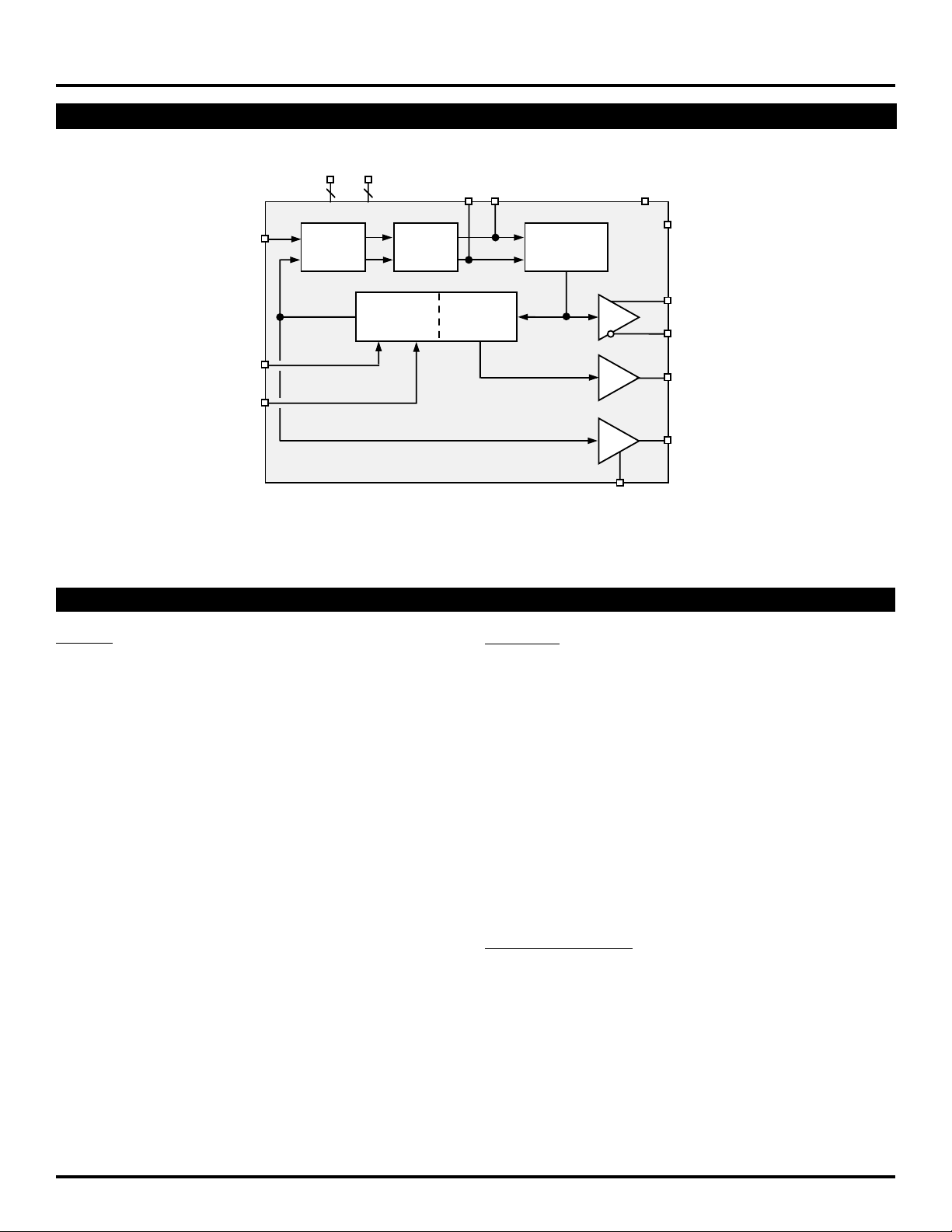
FUNCTIONAL BLOCK DIAGRAM
V
CCA
GND
57
FLTRP/N
V
ClockWorks™
SY89426
CCO
PIN DESCRIPTION
INPUTS
RFCK
(TTL)
SEL39
(TTL)
SEL78
(TTL)
Φ/f
CHG
PUMP
FEEDBACK
÷ 2/3/4
DIVIDER
÷ 4
OUTPUTS
622MHz
VCO
RST
(TTL)
CK622P
(PECL)
CK622N
CK155
(PECL)
RETRFCK
(TTL)
DISC
(TTL)
RFCK [Reference Clock] TTL
Reference clock IN. (38.88, 51.84 or 77.76MHz).
SEL39 [38.88MHz Select] TTL
Logic HIGH on this pin denotes a 38.88MHz input reference
clock. Tie to logic LOW if input is not 38.88MHz.
SEL78 [77.76MHz Select] TTL
Logic HIGH on this pin denotes a 77.76MHz input reference
clock. Tie to logic LOW if input is not 77.76MHz.
RST [Reset] TTL
Tie to logic LOW for normal operation; logic HIGH forces reset
of internal Phase Detector & feedback dividers.
FLTRP, FLTRN [Loop Filter, Pos & Neg] Analog
Connect a series RC loop filter between these pins. The
suggested RC values are 500Ω and 0.1µF, as shown in the
Typical Application.
DISC [Disable Clock] TTL
Logic HIGH on this pin disables the Retimed Reference Clock
output RETRFCK); if this output is not required, it is
recommended that it be disabled to reduce switching noise. A
logic LOW enables the output.
CK622P, CK622N [622 Clock Output] Differential PECL.
622.08MHz output clock from PLL B.
CK155 [155 Clock Out] Single-ended PECL
155.52MHz output clock.
RETRFCK [Retimed Reference Clock Out] TTL
An output clock with the same frequency as the input Reference
Clock (RFCK) and a 45-55% duty cycle. This output is derived
by dividing the 622.08MHz output by the appropriate factor
(e.g., divide by 16 for a 38.88MHz inout reference; divide by
12 for 51.84Mhz in; or divide by 8 for 77.76MHz in).
POWER & GROUND
VCC +5V for internal circuits.
VCCO +5V for PECL outputs.
GND Ground (0 volts).
2
 Loading...