

MICREL SY89425 Datasheet
DUAL SONET OC-12
(
)
(
)
(
)
P
CLOCK SYNTHESIZER
ClockWorks™
SY89425
FEATURES
■ Two independently-powered 622.08MHz clock
sources one chip
■ Differential PECL outputs
■ TTL/CMOS compatible inputs
■ SONET compliant jitter performance (≤0.01UI)
■ Choice of three reference frequencies for each PLL
■ Only 395mW per PLL (typ)
■ Complies with Bellcore, CCITT and ANSI standards
■ Single +5 volt power supply
■ Fully compatible with industry standard 10KH I/O
levels
■ Available in 28-pin PLCC package
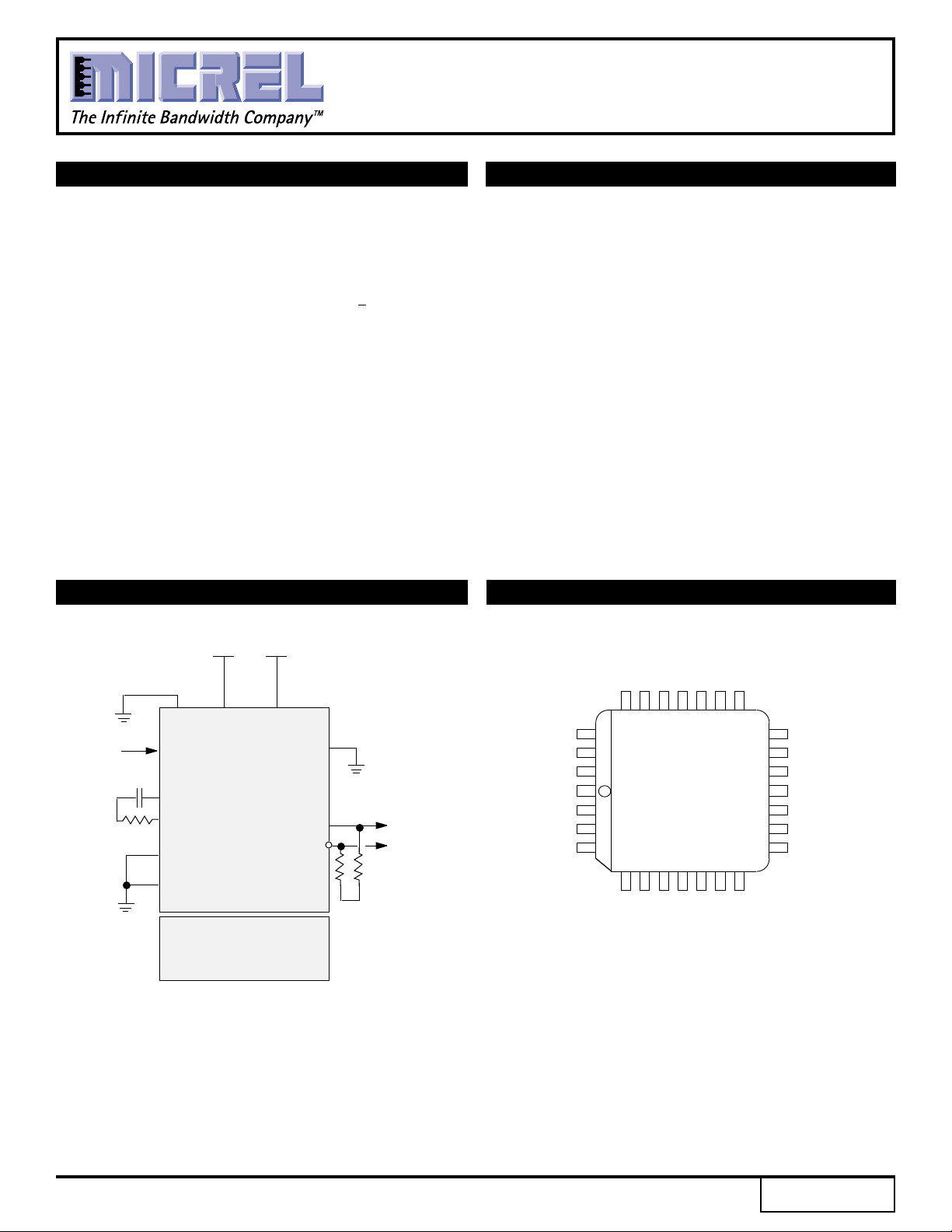
TYPICAL APPLICATION
DESCRIPTION
Micrel-Synergy's SY89425 Dual Phase Locked Loop
(PLL) consists of two totally separate, SONET compliant
622.08MHz clock generators on one chip. The user may
select to power both PLLs or PLL A only. Each PLL
produces a low-jitter OC-12/STS-12 clock rate from an
input reference clock of 38.88, 51.84, or 77.76MHz. When
using both PLLs, it is not necessary that they share a
common reference clock (e.g., PLL A may operate from an
STS-1 reference of 51.84MHz, while PLL B operates from
an OC-3/STS-3 reference of 77.76MHz).
The SY89425 operates from a single +5 volt supply, and
requires only a simple series RC loop filter for each PLL.
Coupling Micrel-Synergy's advanced PLL technology
with our proprietary ASSET™ bipolar process has produced
a clock generator IC which exceeds applicable Bellcore
and ANSI specifications, while setting a new standard for
performance and flexibility.
PIN CONFIGURATION
CLOCK IN
0.1uF
500Ω
+5V +5V
VCCA VCCOA
GND
RFCKA
TTL
FLTRAN
FLTRAP
SEL39A
(TTL)
SEL78A
TTL
PLL A
PLL B
GND AGND
(SAME AS PLL A)
RSTA
TTL
CK622A
(PECL)
CK622AN
+3V
622.08MHz
2X 50Ω
SEL39A
SEL78A
RFCKA
CCA
V
RFCKB
SEL78B
SEL39B
GND
25 24 23 22 21 20 19
26
27
28
1
2
3
4
567891011
GND
GND
RSTA
PLCC
TOP VIEW
GND
RSTB
FLTRAP
FLTRBP
CCA
V
FLTRAN
VCCB
FLTRBN
CCA
V
VCCB
18
CK622AP
17
CK622AN
V
16
15
14
13
12
CCOA
GND
VCCOB
CK622BN
CK622BP
1
Rev.: E Amendment: /0
Issue Date: August, 1998
Micrel
(8/12/16)
(8/12/16)
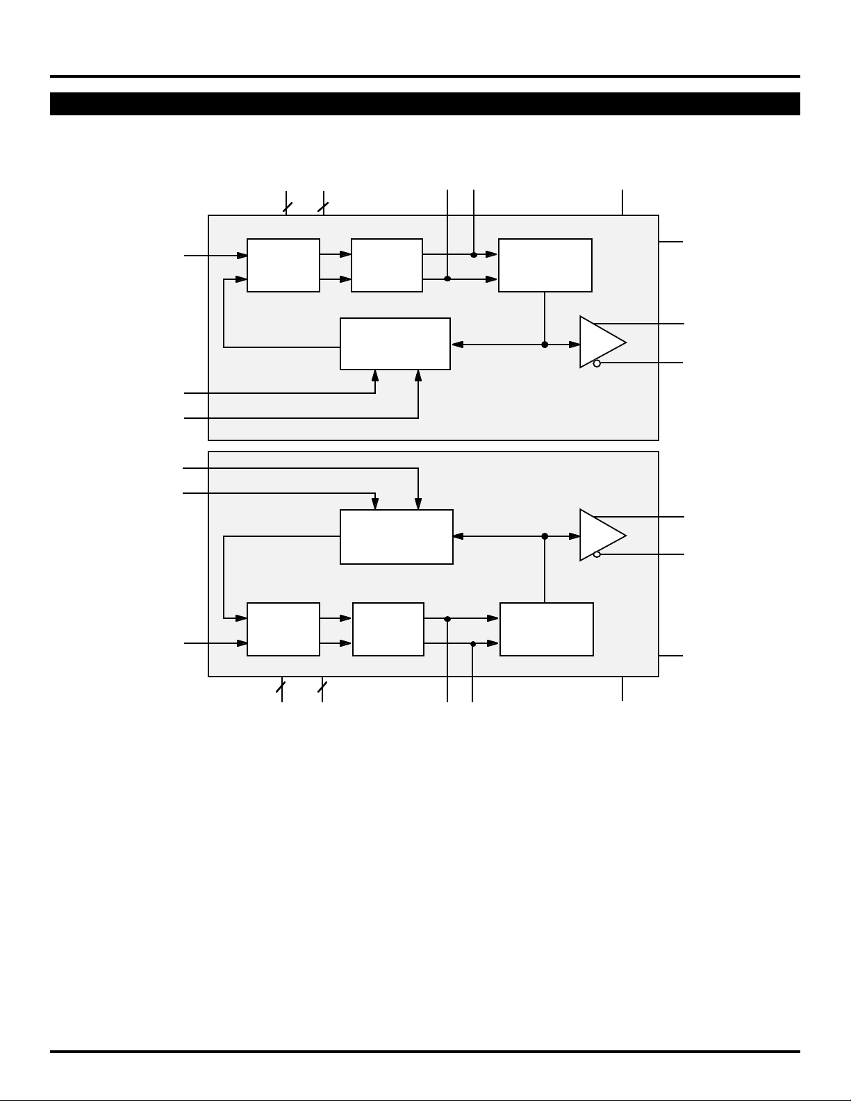
FUNCTIONAL BLOCK DIAGRAM
ClockWorks™
SY89425
RFCKA (TTL)
SEL39A (TTL)
SEL78A (TTL)
SEL78B (TTL)
SEL39B (TTL)
V
23
GND FLTRAP/N
CCA
Φ/f
CHG
PUMP
FEEDBACK
DIVIDER
FEEDBACK
DIVIDER
622MHz
VCO
PLL A
PLL B
V
CCOA
RSTA (TTL)
CK622AP
(PECL)
CK622AN
CK622BP
(PECL)
CK622BN
RFCKB (TTL)
Φ/f
32
V
GND FLTRBP/N
CCB
CHG
PUMP
622MHz
VCO
V
CCOB
RSTB (TTL)
2
Micrel
PIN DESCRIPTION
ClockWorks™
SY89425
INPUTS
RFCKB [Reference Clock B] TTL
Reference clock in for PLL B. (38.88, 51.84 or 77.76MHz).
SEL39B [38.88MHz Select B] TTL
Logic HIGH on this pin denotes a 38.88MHz input reference
clock for PLL B. Tie to logic LOW if input is not 38.88MHz.
SEL78B [77.76MHz Select B] TTL
Logic HIGH on this pin denotes a 77.76MHz input reference
clock for PLL A. Tie to logic LOW if input is not 77.76MHz.
RSTB [Reset B] TTL
Tie to logic LOW for normal operation; logic HIGH forces reset
of internal Phase Detector & feedback dividers on PLL B.
FLTRBP, FLTRBN (Loop Filter B, Pos & Neg) Analog.
Connect a series RC loop filter between these pins. The
suggested loop filter is 0.1µF and 500 ohms, as shown in the
typical application on page 3-9.
RSTA (Reset A) TTL
Tie to logic LOW for normal operation; logic HIGH forces reset
of internal Phase Detector & feedback dividers on PLL A.
REFCKA [Reference Clock A] TTL
Reference clock in for PLL A.
FLTRAP, FLTRAN (Loop Filter A, Pos & Neg) Analog.
Connect a series RC loop filter between these pins. The
suggested loop filter is 0.1µF and 500 ohms, as shown in the
typical application on page 5-527.
OUTPUTS
CK622BP, CK622BN (Clock Out B) Differential PECL
622.08MHz output clock from PLL B.
CK622AP, CK622AN (Clock Out A) Differential PECL
622.08MHz output clock from PLL A.
POWER & GROUND
VCCA +5V for PLL A.
VCCB +5V for PLL B.
VCCOA +5V for PLL A PECL outputs.
VCCOB +5V for PLL B PECL outputs.
GND Ground (0 volts)
SEL78A [77.76MHz Select A] TTL
REFERENCE FREQUENCY SELECTION
Logic HIGH on this pin denotes a 77.76MHz input reference
clock for PLL A. Tie to logic LOW if input is not 77.76MHz.
SEL39A [38.88MHz Select A] TTL
Logic HIGH on this pin denotes a 38.88MHz input reference
clock for PLL A. Tie to logic LOW if input is not 38.88MHz.
ABSOLUTE MAXIMUM RATINGS
Symbol Parameter Rating Unit
VCC Power Supply 0 to +7 V
VI Input Voltage 0 to VCC V
IOUT Output Current –Continuous 50 mA
TA Operatimg Temperature Range 0 to +85 °C
T
store Storage Temperature Range –65 to +150 °C
NOTE:
1. Permanent device damage may occur if ABSOLUTE MAXIMUM RATINGS are exceeded. This is a stress rating only and functional operation is not
implied at conditions other than those detailed in the operational sections of this data sheet. Exposure to ABSOLUTE MAXIMUM RATING conditions
for extended periods may affect device reliability.
(1)
–Surge 100
SEL39 SEL78 fRFCK
0 0 51.84
0 1 77.76
1 0 38.88
1 1 77.76
3
 Loading...