

Micrel SY89228U User Manual
查询SY89228UMG供应商
General Description
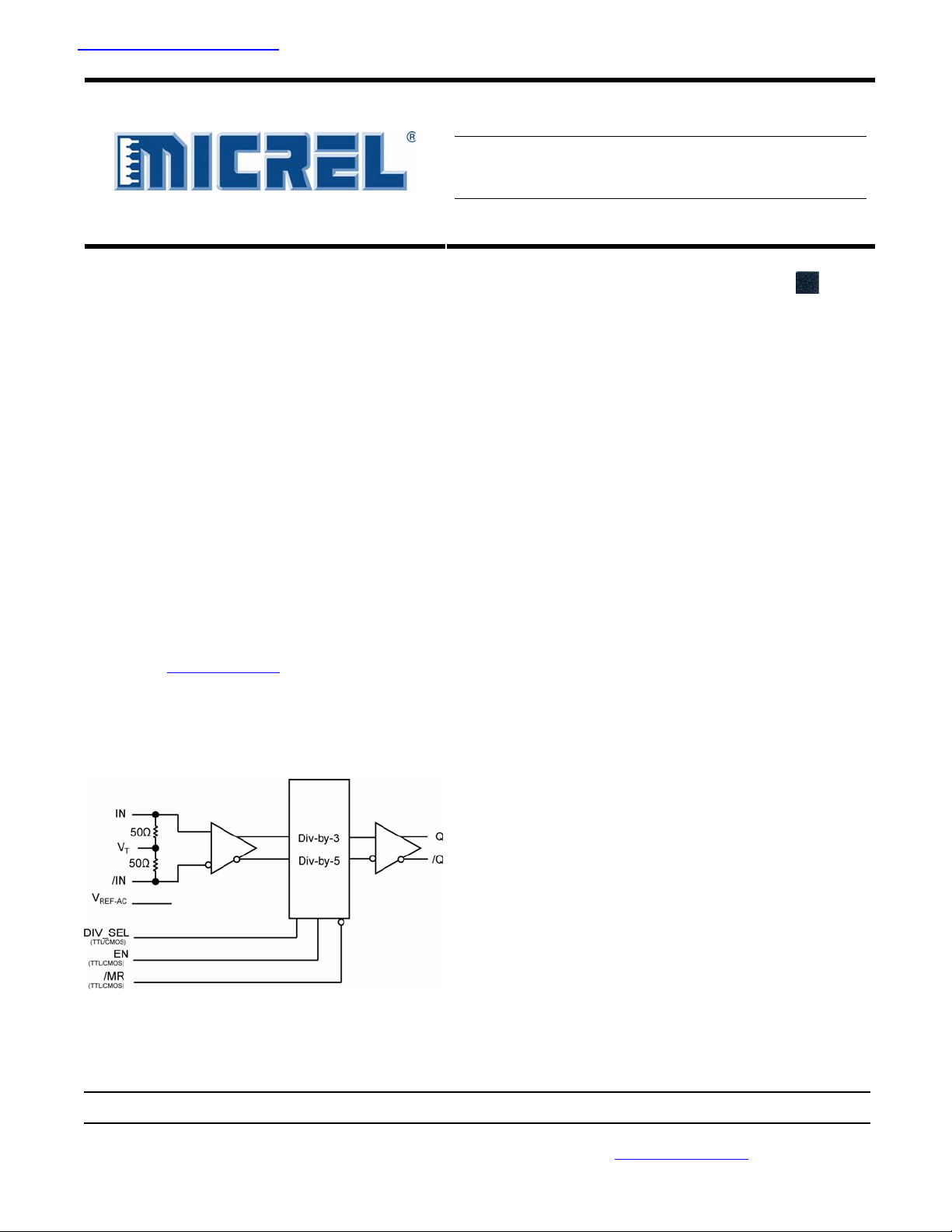
The SY89228U is a precision, low jitter 1GHz ÷3, ÷5
clock divider with an LVPECL output. A unique FailSafe Input (FSI) protection prevents metastable
output conditions when the input clock voltage swing
drops significantly below 100mV or input is removed.
The differential input includes Micrel’s unique, 3-pin
internal termination architecture that allows the input
to interface to any differential signal (AC- or DCcoupled) as small as 100mV (200mV
level shifting or termination resistor networks in the
signal path. The outputs are 800mV, 100Kcompatible LVPECL with fast rise/fall times
guaranteed to be less than 270ps.
The SY89228U operates from a 2.5V ±5% or 3.3V
±10% supply and is guaranteed over the full
industrial temperature range of –40°C to +85°C. The
SY89228U is part of Micrel’s high-speed, Precision
®
Edge
product line.
All support documentation can be found on Micrel’s
web site at: www.micrel.com
.
) without any
PP
Block Diagram
SY89228U
1GHz Precision, LVPECL ÷3, ÷5 Clock Divider
with Fail-Safe Input and Internal Termination
Precision Edge®
Features
• Accepts a high-speed input and provides a precision
÷3 and ÷5 sub-rate, LVPECL output
• Fail-Safe Input
– Prevents oscillations when input is invalid
• Guaranteed AC performance over temperature and
supply voltage:
– DC-to >1.0GHz throughput
– < 1500ps Propagation Delay (In-to-Q)
– < 270ps Rise/Fall times
• Ultra-low jitter design:
– <1ps
– <1ps
– <10ps
– <0.7ps
• Unique patented internal termination and VT pin
accepts DC- and AC-coupled inputs (CML, PECL,
LVDS)
• Wide input voltage range VCC to GND
• 800mV LVPECL output
• 46% to 54% Duty Cycle(÷ 3)
• 47% to 53% Duty Cycle(÷ 5)
• 2.5V ±5% or 3.3V ±10% supply voltage
• -40°C to +85°C industrial temperature range
• Available in 16-pin (3mm x 3mm) MLF
random jitter
RMS
cycle-to-cycle jitter
RMS
total jitter (clock)
PP
MUX crosstalk induced jitter
RMS
®
package
Applications
• Fail-safe clock protection
Markets
• LAN/WAN
• Enterprise servers
Precision Edge is a registered trademark of Micrel, Inc.
MLF and MicroLeadFrame are registered trademarks of Amkor Technology.
Micrel Inc. • 2180 Fortune Drive • San Jose, CA 95131 • USA • tel +1 (408) 944-0800 • fax + 1 (408) 474-1000 • http://www.micrel.com
August 2007
• ATE
• Test and measurement
hbwhelp@micrel.com
M9999-080707-A
or (408) 955-1690
Micrel, Inc. SY89228U
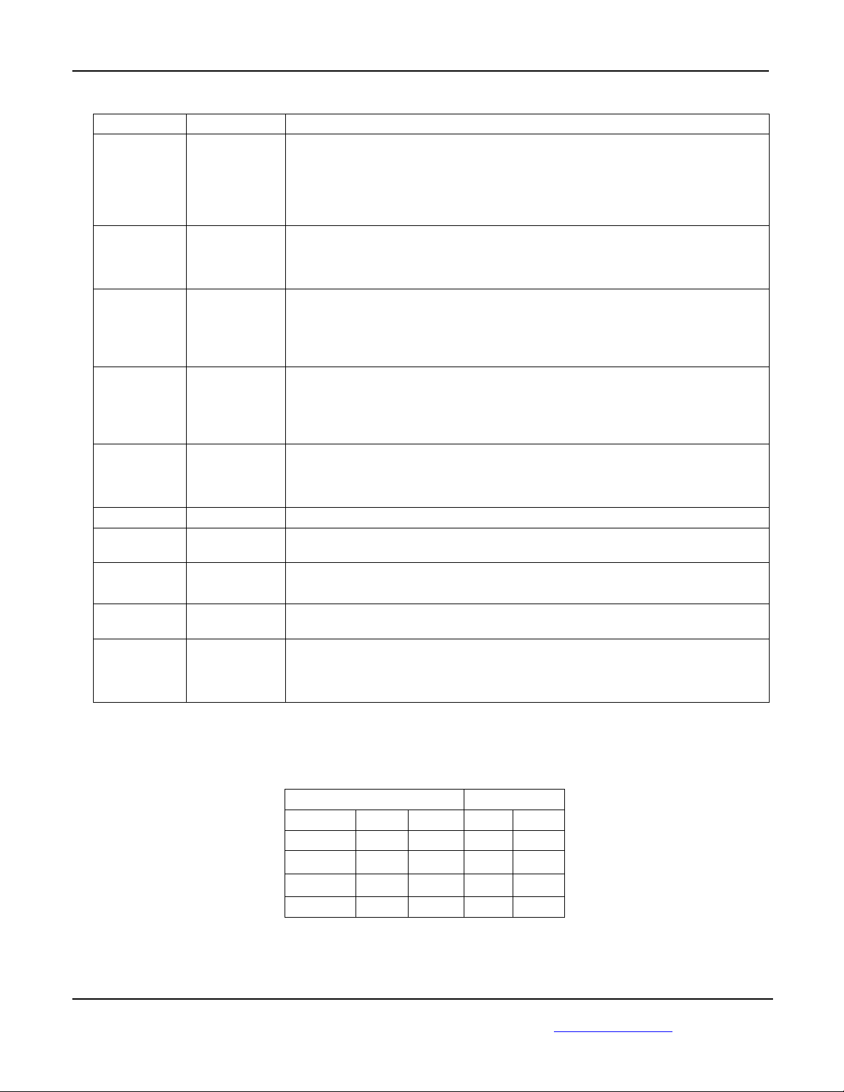
Ordering Information
(1)
Part Number
SY89228UMG MLF-16 Industrial
SY89228UMGTR
Notes:
1. Contact factory for die availability. Dice are guaranteed at T
2. Tape and Reel.
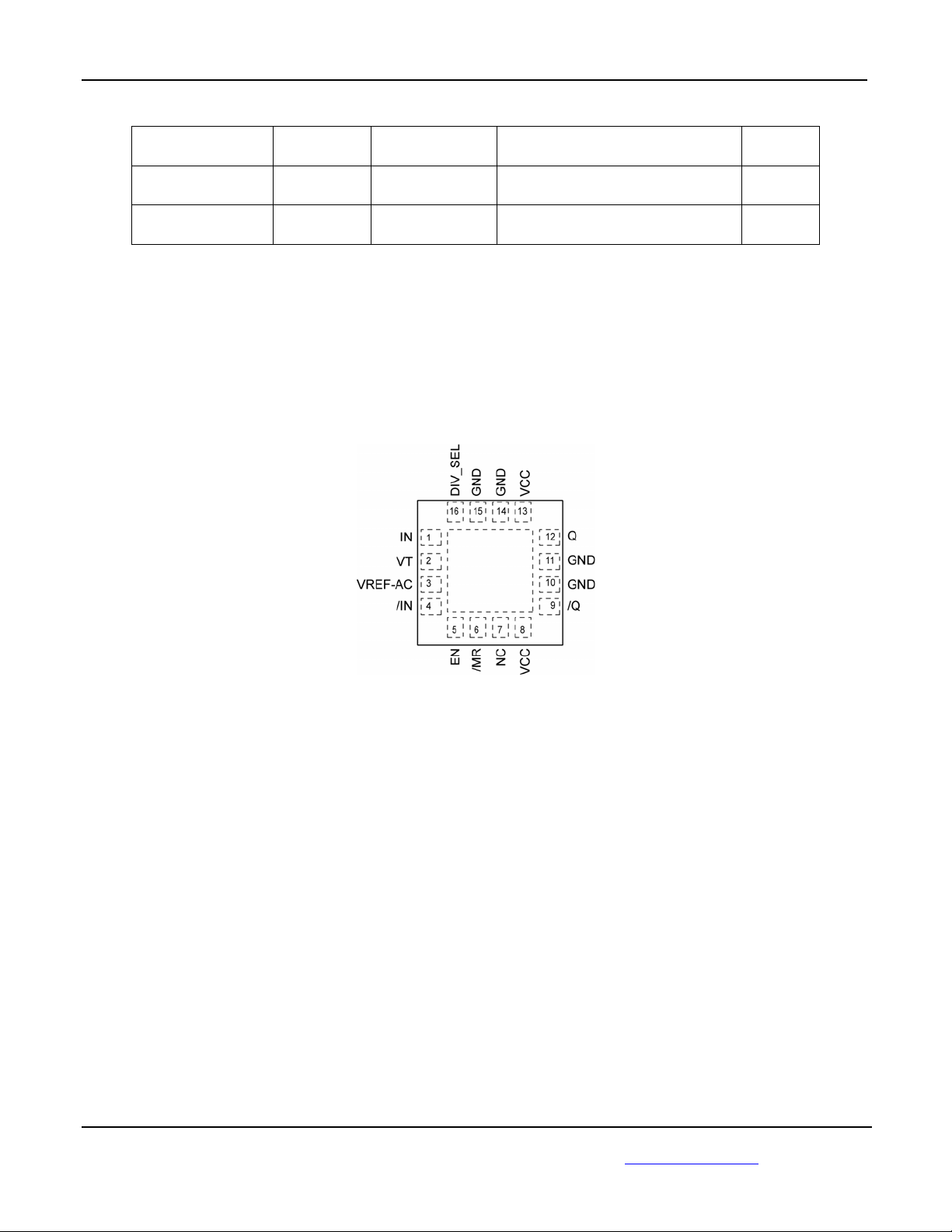
Pin Configuration
Package
Type
(2)
MLF-16 Industrial
Operating
Range
Package Marking
228U with
Pb-Free bar-line Indicator
228U with
Pb-Free bar-line Indicator
= 25°C, DC Electricals Only.
A
Lead
Finish
NiPdAu
Pb-Free
NiPdAu
Pb-Free
16-Pin MLF® (MLF-16)
August 2007 M9999-080707-A
2
hbwhelp@micrel.com
or (408) 955-1690
Micrel, Inc. SY89228U
Pin Description
Pin Number Pin Name Pin Function
1, 4 IN, /IN
2 VT
3 VREF-AC
5 EN
6 /MR
7 NC No Connect
8, 13 VCC
12, 9 Q, /Q
10, 11, 14,15
16 DIV_SEL
GND,
Exposed Pad
Differential Input: This input pair is the differential signal input to the device, which
accepts AC- or DC-coupled signal as small as 100mV. The input internally terminates
to a VT pin through 50 and has level shifting resistors of 3.72 k to VCC. This
allows a wide input voltage range from VCC to GND. See Figure 3a, Simplified
Differential Input Stage for details. Note that this input will default to a valid (either
HIGH or LOW) state if left open. See “Input Interface Applications” subsection.
Input Termination Center-Tap: Each side of the differential input pair terminates to
the VT pin. The VT pin provides a center-tap for the input (IN, /IN) to a termination
network for maximum interface flexibility. See “Input Interface Applications”
subsection for more details.
Reference Voltage: This output biases to V
IN and /IN. Connect VREF-AC directly to the VT pin. Bypass with 0.01µF low ESR
capacitor to VCC. Due to limited drive capability, the VREF-AC pin is only intended to
drive its respective VT pin. Maximum sink/source current is ±0.5mA. See “Input
Interface Applications” subsection.
Single-ended Input: This TTL/CMOS-compatible input disables and enables the
output. It is internally connected to a 25k pull-up resistor and will default to a logic
HIGH state if left open. When disabled, Q goes LOW and /Q goes HIGH. EN being
synchronous, outputs will be enabled/disabled after a rising and a falling edge of the
input clock. V
Single-ended Input: This TTL/CMOS-compatible input, when pulled LOW,
asynchronously sets Q output LOW and /Q output HIGH. Note that this input is
internally connected to a 25k pull-up resistor and will default to logic HIGH state if
left open. VTH = VCC/2.
Positive Power Supply: Bypass with 0.1µF in parallel with 0.01µF low ESR capacitors
as close to the V
Differential Output: The LVPECL output swing is typically 800mV and is terminated
with 50 to V
Ground: Ground and exposed pad must be connected to a ground plane that is the
same potential as the ground pins.
Single-ended Input: This TTL/CMOS-compatible input selects divide-by-3 when
pulled LOW and divide-by-5 when pulled HIGH. Note that this input is internally
connected to a 25k pull-up resistor and will default to logic HIGH state if left open.
= VCC/2.
V
TH
= VCC/2.
TH
pins as possible.
CC
-2V. See the “Truth Table” below for the logic function.
CC
–1.2V. It is used for AC-coupling inputs
CC
Truth Table
Inputs Outputs
DIV_SEL EN /MR Q /Q
X X 0 0 1
0 1 1
1 1 1
X 0 1 0 1
August 2007 M9999-080707-A
3
÷
3
÷
5
÷
3
÷
5
hbwhelp@micrel.com
or (408) 955-1690
Micrel, Inc. SY89228U
Absolute Maximum Ratings
(1)
Operating Ratings
(2)
Supply Voltage (VCC) ..........................–0.5V to +4.0V
Input Voltage (V
LVPECL Output Current (I
) ..................................–0.5V to V
IN
)....................................
OUT
CC
Continuous ................................................. 50mA
Surge........................................................ 100mA
Current (V
Source or sink current on V
)
T
pin…………±100mA
T
Input Current
Supply Voltage (VCC).................. +2.375V to +2.625V
......................................................+3.0V to +3.6V
Ambient Temperature (T
Package Thermal Resistance
®
(θ
®
(ψ
JA
JB
)
)
MLF
Still-Air ..................................................... 75°C/W
MLF
)................ –40°C to +85°C
A
(3)
Junction-to-Board………………………….33°C/W
Source or sink current on (IN, /IN) ........... ±50mA
Current (V
Source/Sink Current on V
REF-AC
)
REF-AC
(4)
............ ±0.5mA
Maximum Operating Junction Temperature…..125°C
Lead Temperature (soldering, 20 sec.) ..........+260°C
Storage Temperature (T
)..................–65°C to 150°C
s
DC Electrical Characteristics
(5)
TA = –40°C to +85°C, unless otherwise stated.
Symbol Parameter Condition Min Typ Max Units
VCC Power Supply
2.375
3.0
ICC Power Supply Current No load, max VCC 40 55 mA
RIN
R
DIFF_IN
Input Resistance
(IN-to-V
Differential Input Resistance
)
T
45 50 55
90 100 110
(IN-to-/IN)
VIH
Input High Voltage
1.2 V
(IN, /IN)
VIL
Input Low Voltage
0 V
(IN, /IN)
VIN
Input Voltage Swing
See Figure 2a. Note 6. 0.1 V
(IN, /IN)
V
DIFF_IN
Differential Input Voltage Swing
See Figure 2b. 0.2 V
|IN-/IN|
V
IN_FSI
Input Voltage Threshold that
30 100 mV
Triggers FSI
V
Output Reference Voltage VCC–1.3 VCC–1.2 VCC–1.1 V
REF-AC
V
Voltage from Input to VT 1.8 V
T_IN
Notes:
1. Permanent device damage may occur if absolute maximum ratings are exceeded. This is a stress rating only and functional operation is
not implied at conditions other than those detailed in the operational sections of this data sheet. Exposure to absolute maximum rating
conditions for extended periods may affect device reliability.
2. The data sheet limits are not guaranteed if the device is operated beyond the operating ratings.
3. Package thermal resistance assumes exposed pad is soldered (or equivalent) to the devices most negative potential on the PCB. θ
values are determined for a 4-layer board in still air unless otherwise stated.
ψ
JB
4. Due to limited drive capability use for input of the same package only.
5. The circuit is designed to meet the DC specifications shown in the above table after thermal equilibrium has been established.
6. V
(max) is specified when V
IN
is floating.
T
2.5
3.3
2.625
3.6
V
CC
–0.1 V
IH
V
CC
JA
V
V
and
August 2007 M9999-080707-A
4
hbwhelp@micrel.com
or (408) 955-1690
Micrel, Inc. SY89228U
LVPECL Outputs DC Electrical Characteristics
VCC = 2.5V ±5% or 3.3V ±10%; RL = 50 to VCC-2V; TA = –40°C to + 85°C, unless otherwise stated.
Symbol Parameter Condition Min Typ Max Units
VOH
VOL
V
OUT
V
DIFF_OUT
Output HIGH Voltage
Q, /Q
Output LOW Voltage
Q, /Q
Output Voltage Swing
Q, /Q
Differential Output Voltage Swing
Q, /Q
V
V
See Figure 2a. 550 800 950 mV
See Figure 2b. 1100 1600 mV
(7)
-1.145 VCC-0.895 V
CC
-1.945 VCC-1.695 V
CC
LVTTL/CMOS DC Electrical Characteristics
VCC = 2.5V ±5% or 3.3V ±10%; TA = –40°C to + 85°C, unless otherwise stated.
Symbol Parameter Condition Min Typ Max Units
VIH Input HIGH Voltage 2.0 V
VIL Input LOW Voltage 0.8 V
IIH Input HIGH Current -125 30 µA
IIL Input LOW Current -300 µA
Note:
7. The circuit is designed to meet the DC specifications shown in the above table after thermal equilibrium has been established.
(7)
August 2007 M9999-080707-A
5
hbwhelp@micrel.com
or (408) 955-1690
 Loading...