

MICREL SY88993AV Datasheet
5V/3.3V 3.2Gbps HIGH-SPEED
LIMITING POST AMPLIFIER
SY88993AV
FEATURES
■ > 3.2Gbps operation
■ Low noise CML Data Outputs
■ Chatter-Free LOS generation
■ Open Collector TTL LOS output
■ TTL /EN Input
■ Differential PECL inputs for data
■ Single 3.3V or 5V power supply
■ Designed for use with SY88922V and SY88905
■ Available in a tiny 10-pin (3mm) MSOP
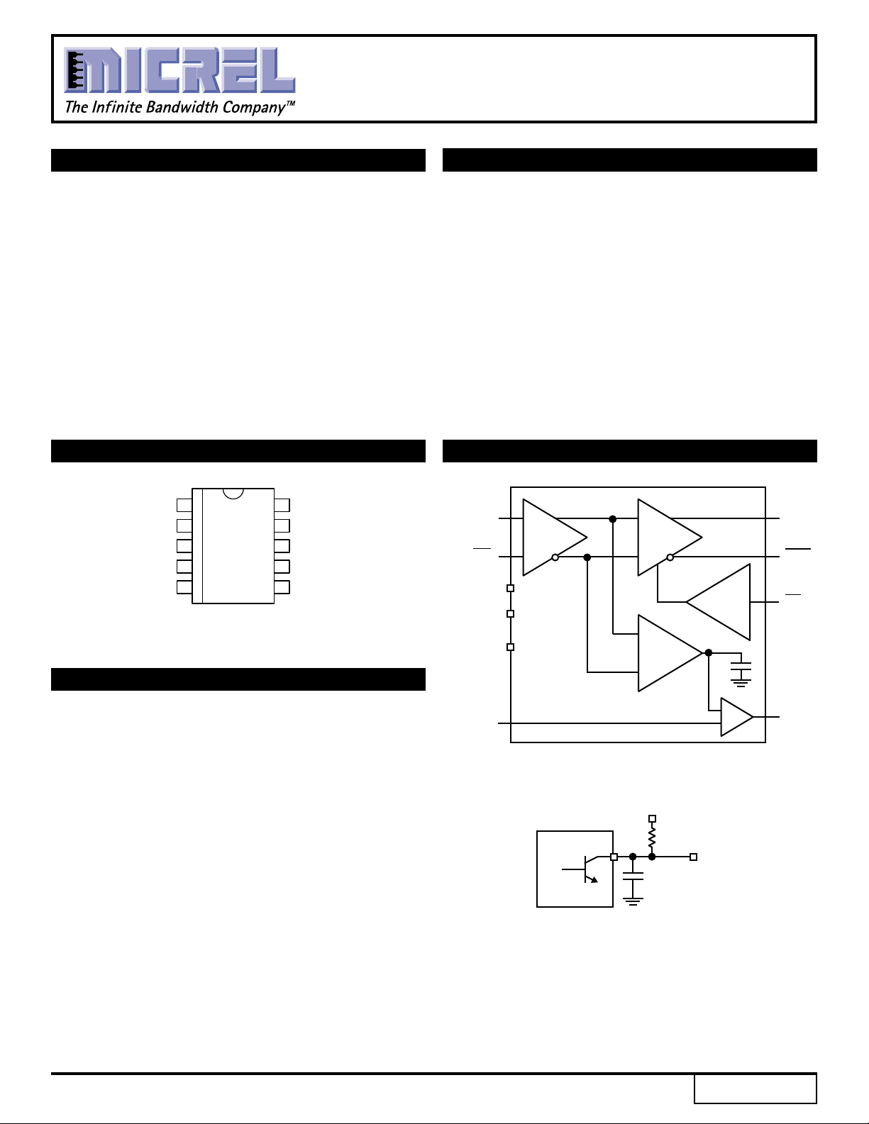
PIN CONFIGURATION
LOS
1/EN
D
IN
2
/D
IN
V
REF
LVL
MSOP
3
K10-1
4
5
10 V
9
8
7
6
CC
D
OUT
/D
OUT
LOS
GND
DESCRIPTION
The SY88993AV limiting post amplifier with its high and
wide bandwidth is ideal for use as a post amplifier in fiberoptic receivers with data rates up to 3.2Gbps. Signals as
small as 4mVp-p can be amplified to drive devices with
CML inputs or AC coupled PECL inputs. The SY88993AV
generates a chatter-free Loss of Signal (LOS) open collector
TTL output.
The SY88993AV incorporates a programmble level detect
function to identify when the input signal has been lost.
This information can be fed back to the /EN input of the
device to maintain stability under loss of signal conditions.
Using LOS
adjusted. The LOS
resistor divider between VCC and V
pin the sensitivity of the level detect can be
LVL
voltage can be set by connecting a
LVL
, Figure 3.
REF
BLOCK DIAGRAM
D
V
D
REF
V
CC
IN
Limiting
Amplifer
IN
CML
Buffer
Enable
D
D
EN
OUT
OUT
APPLICATIONS
■ 1.25Gbps and 2.1Gbps Gigabit Ethernet
■ 531Mbps, 1062Mbps and 2.5Gbps SONET/SDH Fibre
Channel
■ 622Mbps
■ Gigabit interface converter (GBIC)
■ Small Form Factor Trancievers
■ Parallel 10G Ethernet
LOS
GND
LVL
SY88993AV
LOS
Level
Detect
V
CC
4.7k to 10k
LOS
1
Rev.: A Amendment: /1
Issue Date: October, 2000
Micrel
SY88993AV
PIN NAMES
Pin Type Function
D
IN
/D
IN
LOS
/EN TTL Input Output Enable (Active Low)
LOS TTL Output Loss of Signal Indicator
GND Ground Ground
D
OUT
/D
OUT
V
CC
V
REF
ABSOLUTE MAXIMUM RATINGS
LVL
Data Input Data Input
Data Input Inverting Data Input
Input Loss of Signal Level Set
(Open Collector) (Active High)
CML Output Data Output
CML Output Inverting Data Output
Power Supply Positive Power Supply
Output Reference Voltage Output
for LOS Level Set (see Fig. 3)
(1)
GENERAL DESCRIPTION
General
The SY88993AV is an integrated limiting amplifier
intended for high-frequency fiber-optic applications. The
circuit connects to typical transimpedance amplifiers found
within a fiber-optics link. The linear signal output from a
transimpedance amplifier can contain significant amounts
of noise, and may vary in amplitude over time. The
SY88993AV limiting amplifier quantizes the signal and
outputs a voltage-limited waveform.
The /EN pin allows the user to disable the output signal
without removing the input signal.
Symbol Rating Value Unit
V
CC
DIN, /D
IN
T
A
T
store
NOTE:
1. Permanent device damage may occur if ABSOLUTE MAXIMUM RATINGS are exceeded. This is a stress rating only and functional operation is not implied
at conditions other than those detailed in the operational sections of this data sheet. Exposure to ABSOLUTE MAXIMUM RATlNG conditions for extended
periods may affect device reliability.
Power Supply Voltage 0 to +7.0 V
Input Voltage 0 to V
CC
Operating Temperature Range –40 to +85 °C
Storage Temperature Range –55 to +125 °C
V
2
Micrel
SY88993AV
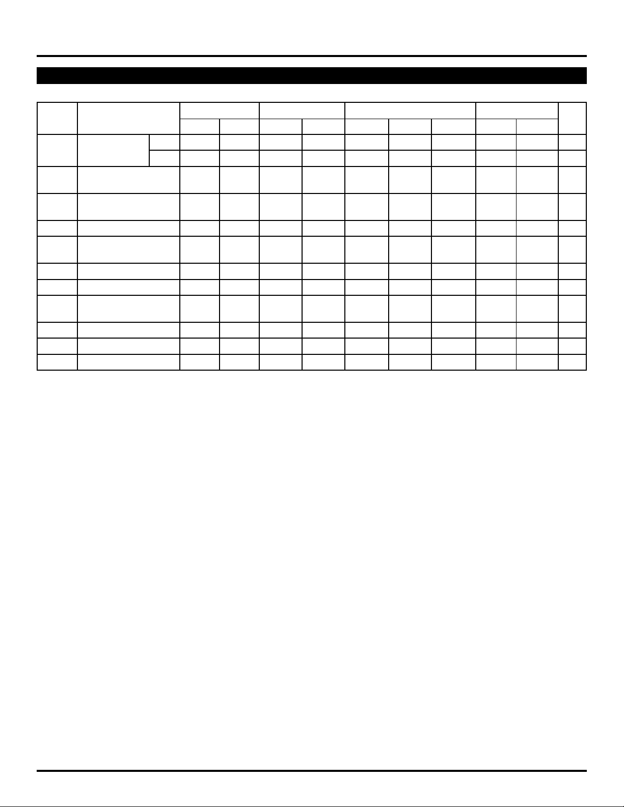
DC ELECTRICAL CHARACTERISTICS
VCC = +3.3V ±10% or +5V ±10%, R
Symbol Parameter Min. Max. Min. Max. Min. Typ. Max. Min. Max. Unit
I
CC
I
IL
I
IH
I
OH
V
OFFSET
V
CMR
LOS
V
OL
V
REF
V
IH
V
IL
NOTES:
1. No output load. VCC = 5V ±10% or 3.3V ±10%
2. VOH = 5.5V.
3. IOL = +2mA.
4. VIN = 0.5V
5. VIN = 2.7V
6. VIN = V
Power Supply 5.0V — 55 — 55 — 43 55 — 65 mA
(1)
Current
3.3V — 50 — 50 — 40 50 — 60 mA
/EN Input LOW –0.3
Current
/EN Input HIGH — 20
Current — 100
LOS Output Leakage
(2)
Differential Output — ±80 — ±80 — ±9 ±80 — ±80 mV
Offset
Common Mode Range GND±2VCC–0.2 GND±2VCC–0.2 GND±2V
LVL
LOS
Level V
LVL
LOS Output Low — 0.5 — 0.5 — — 0.5 — 0.5 V
(3)
Level
Reference Voltage
VCC –1.38 VCC –1.26 VCC –1.38 VCC –1.26 VCC –1.38 VCC –1.32 VCC –1.26 VCC –1.38 VCC –1.26
/EN Input HIGH Voltage 2.0 — 2.0 — 2.0 — — 2.0 — V
/EN Input LOW Voltage — — 0.8 — 0.8 — — 0.8 — V
CC
= 50Ω to V
LOAD
A = –40°CTA = 0°CTA = +25°CTA = +85°C
T
(4)
— –0.3
(5)
(6)
CC
(4)
—20
— 100
— –0.3
(5)
(6)
(4)
——20
— — 100
— — –0.3
(5)
(6)
(4)
—20
— 100
—mA
(5)
(6)
— 100 — 100 — — 100 — 100 uA
–0.2 GND±2VCC–0.2 V
CC
REF
V
CC
V
REF
V
CC
V
REF
—VCCV
REF
V
CC
µA
V
V
3
 Loading...