

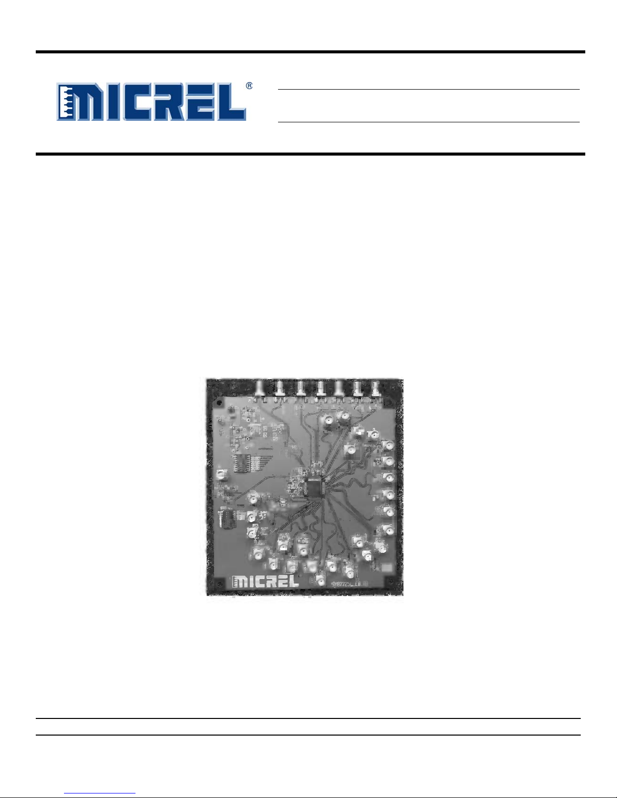
2.5Gbps GPON/BPON ONU SERDES
SY87725L Evaluation Board
Micrel Inc. • 2180 Fortune Drive • San Jose, CA 95131 • USA • tel +1 (408) 944-0800 • fax + 1 (408) 474-1000 • http://www.micrel.com
July 2008
M9999-071108-B
General Description
The SY87725L evaluation board is designed for
convenient setup and quick evaluation of the SY87725L
using a single power source. The evaluation board is
optimized to interface directly to 50Ω test equipment since
the evaluation board is configured with AC-coupled inputs
and AC-coupled outputs.
All datasheets and support documentation can be found
on Micrel’s web site at: www.micrel.com.
Features
∑ Single +3.3V power supply
∑ AC-coupled configuration for direct interface with 50Ω
test equipment
∑ 2.5G/1.25G/625M down stream
∑ 1.25G/625M/156M up stream
Related Documentation
∑ SY87725L, 2.5Gbps GPON/BPON ONU Serdes
Datasheet
__________________________________________________________________________________________
Evaluation Board
Micrel, Inc.
SY87725L Evaluation Board
July 2008
2
M9999-071108-B
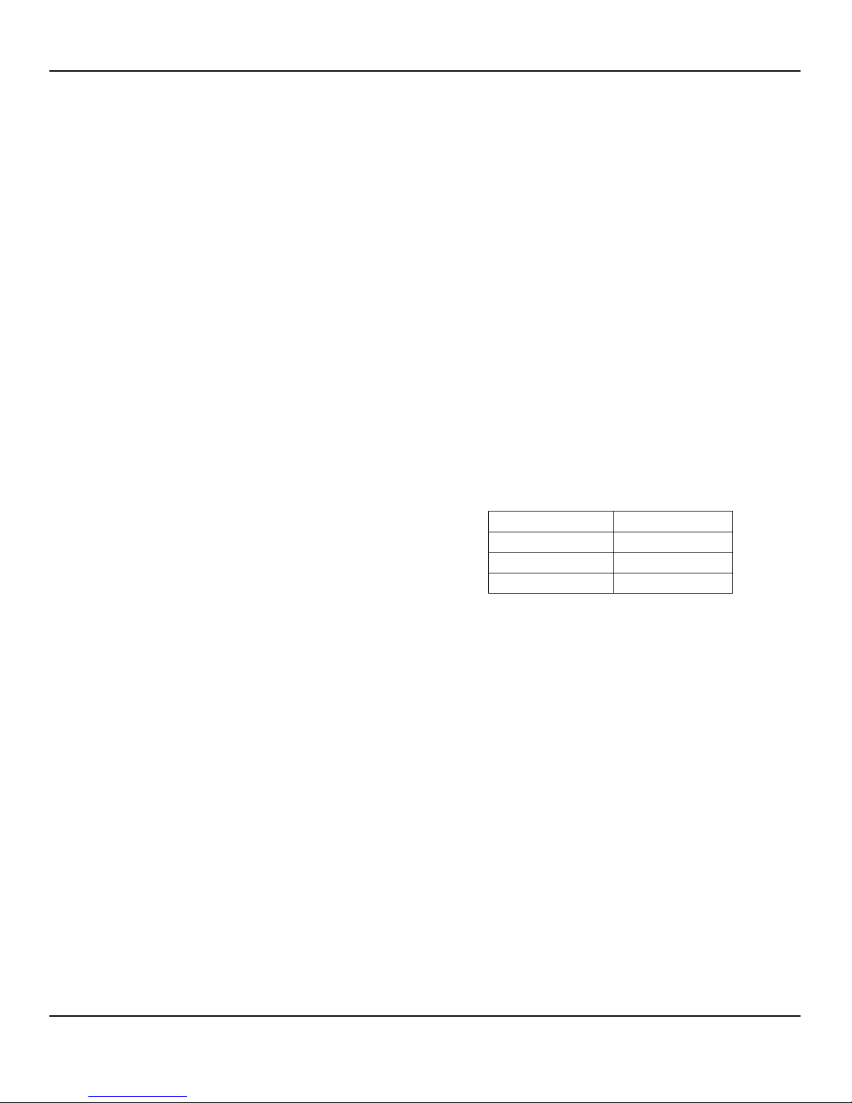
Evaluation Board Description
AC-Coupled Evaluation Board
The SY87725L is 64-pin EPAD-TQFP package. The
evaluation board is designed to operate with a single 3.3V
±10% power supply and is configured with AC-coupled
inputs and outputs. The high-speed input and output
channels are brought out to SMA connectors through
matched-length AC-coupled differential strip-line traces.
AC-Coupled Input
For ease of use, the AC-coupled inputs are biased onboard. The user need only supply the appropriate input
swing to the board.
AC-Coupled Output
The SY87725L is configured with AC-coupled outputs
allowing the board to interface directly with 50Ω
equipment. AC-coupling allows the board to use a single
power supply.
Unused Output
Single-Ended to Scope
Unused complimentary outputs should be terminated into
50Ω-to-ground to prevent unwanted reflections.
AC-Coupled Evaluation Board Setup
Setting up the SY87725L AC-Coupled Evaluation
Board
1. Set the voltage on a DC supply to +3.3V and
turn off the supply. Connect the GND terminal to
the negative side of a DC power supply.
Connect the VCC terminal to the positive side of
a DC power supply.
2. For a LVPECL input signal, set VT to VCC–2.0V.
3. Signal Generator: Using a differential signal
source, set the amplitude of each side of the
differential pair to 400mV (800mV measured
differentially). Set the offset to a positive value,
the value of the offset is not critical, since the
AC-coupled inputs will be automatically biased.
Turn off the outputs of the signal source.
4. I/O Cable Interface: Using equal length 50Ω
impedance coaxial cables connect the signal
source to the inputs on the evaluation board.
Using equal length 50Ω impedance coaxial
cables connect the outputs of the evaluation
board to the oscilloscope of another
measurement device that has an internal 50Ω
termination. Unequal length cables are not
recommended since they introduce duty cycle
distortion and unwanted signal delays.
5. Connect the trigger input of the scope to the
trigger output of the signal generator.
6. Set the evaluation board dipswitch to the
appropriate input selection.
7. Enable the signal source, turn on the DC source,
and monitor the outputs.
Evaluation Board Layout
PC Board Layout
The evaluation boards are constructed with Rogers 4003
material and are coplanar in design fabricated to minimize
noise, achieve high bandwidth and minimize crosstalk.
L1
GND and Signal
L2
GND
L3
VCC
L4
GND
Table 1. Layer Stack
Micrel, Inc.
SY87725L Evaluation Board
July 2008
3
M9999-071108-B
Evaluation Board Schematic

Micrel, Inc.
SY87725L Evaluation Board
July 2008
4
M9999-071108-B
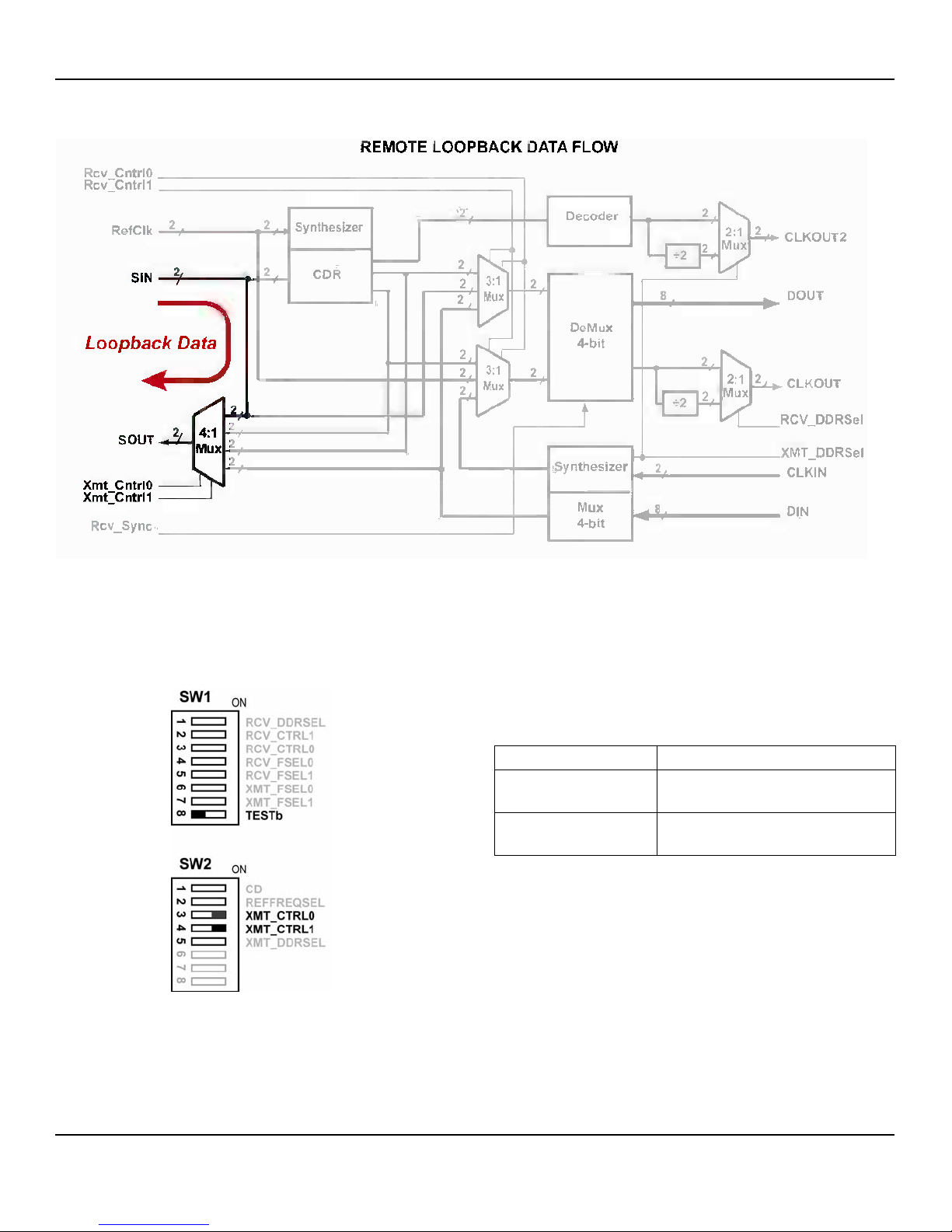
How to Use this Document
The following pages show the individual test modes built
into the SY87725L. The diagram for each mode shows
the main data flow for that mode. The table of required
switch settings lists the switch settings for that mode;
unlisted switch settings are not used in that mode. The
diagram to the left of the table shows the actual dip switch
settings as they would appear on the evaluation board.
The dip switches are configured with a pull-up resistor on
the output so when the switch is in the “OFF” position the
output is HIGH and when the switch is in the “ON”
position the output is pulled to ground, LOW.
The test flow diagram in the Appendix lists the modes in
order from the minimum functionality to the full
configuration. This allows the user to start with the
simplest configuration and progress to the full
configuration.
Micrel, Inc.
SY87725L Evaluation Board
July 2008
5
M9999-071108-B
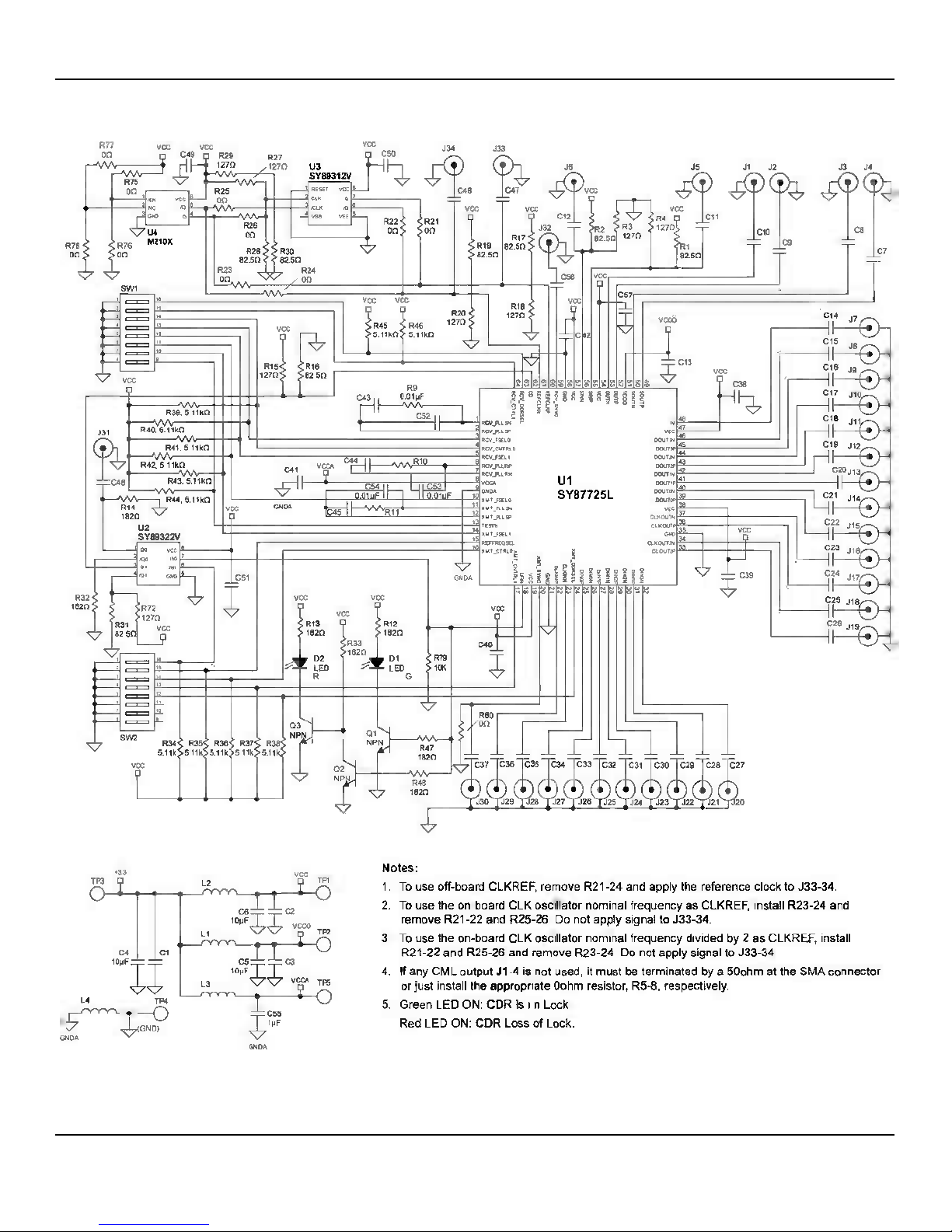
Remote Loopback Data
This is the most basic test mode. It loops back the data
from SIN to SOUT and is used to verify the connections to
SIN and SOUT as well as the power supply connections
to the evaluation board. The SOUT output can be
monitored with a scope or a serial BERT.
Figure 1. Switch Settings for Remote Loopback Data
Switch Settings
Function
TESTb = 1
Disables factory test mode
(enables normal operation)
XMT_CTRL0/1 = 00
Selects the remote loopback
mode so SDOUT = SDIN
Table 2. Required Switch Settings for
Remote Loopback Data Flow

Micrel, Inc.
SY87725L Evaluation Board
July 2008
6
M9999-071108-B
Remote Loopback Recovered Clock
Verifies correct operation of the receive CDR. A RefClk of
155.52MHz or 77.76MHz (selected by REFFREQSEL)
must be supplied for the CDR to function. When CD is
HIGH, the recovered clock coming out of SOUT will be
synchronous and at the same data rate as the data
coming into SIN. When CD is LOW, the clock coming out
of SOUT will be synchronous with the RefClk source.
Figure 2. Switch Settings for Remote Loopback
Recovered Clock
Switch Settings
Function
RCV_FSEL0/1 = 11
Sets receive CDR frequency to
2.48832Gbps (For other
frequencies, refer to Receive
Frequency Selection Table on
page 7 of SY87725L
Datasheet.)
TESTb = 1
Disables factory test mode
(enables normal operation)
CD = 1
Enables clock and data
recovery
REFFREQSEL = 1
Selects RefClk of 155.52MHz
(Set to “0” for 77.76MHz
RefClk)
XMT_CTRL0/1 = 10
Selects the remote loopback
mode so SDOUT = recovered
clock
Table 3. Required Switch Settings for
Remote Loopback Recovered Clock Flow
Micrel, Inc.
SY87725L Evaluation Board
July 2008
7
M9999-071108-B
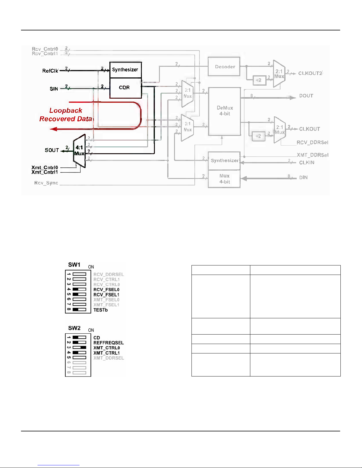
Remote Loopback Recovered Data
Verifies correct operation of the receive CDR. A RefClk of
155.52MHz or 77.76MHz (selected by REFFREQSEL)
must be supplied for the CDR to function. When CD is
HIGH, the recovered data coming out of SOUT will be the
same data coming into SIN (retimed). CDR operation can
be verified with a serial BERT.
Figure 3. Switch Settings for Remote Loopback
Recovered Data
Switch Settings
Function
RCV_FSEL0/1 = 11
Sets receive CDR frequency to
2.48832Gbps (For other
frequencies, refer to Receive
Frequency Selection Table on
page 7 of SY87725L Data
sheet.)
TESTb = 1
Disables factory test mode
(enables normal operation)
CD = 1
Enables clock and data recovery
REFFREQSEL = 1
Selects RefClk of 155.52MHz
XMT_CTRL0/1 - 01
Selects the remote loopback
mode so SDOUT = recovered
data
Table 4. Required Switch Settings for
Remote Loopback Recovered Data Flow
Micrel, Inc.
SY87725L Evaluation Board
July 2008
8
M9999-071108-B
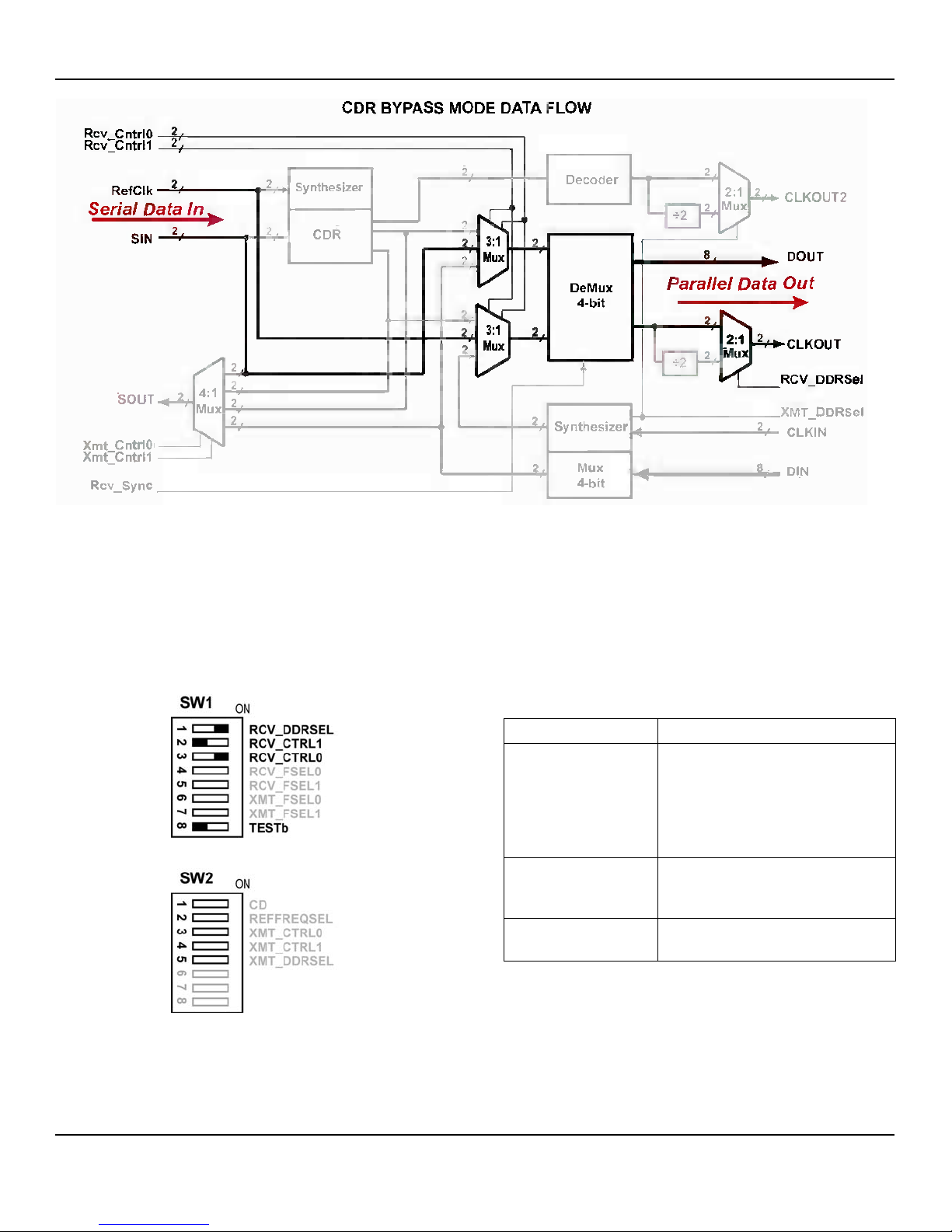
CDR Bypass Mode
Verifies correct operation of the receive DeMux. In this
mode the CDR is bypassed so the serial data coming into
SIN must be clocked in by the serial clock coming into the
RefClk input. In this mode only, the RefCLK will be
155.52MHz or 77.76MHz and must be at the same
rate as the Serial Data In (SIN). For example, if REFCLK
is 155.52MHz, then SIN must be at 155.52Mbps. The 4bit parallel data at the output of DOUT0-3 can be verified
with a parallel BERT.
Figure 4. Switch Settings for CDR Bypass Mode
Switch Settings
Function
RCV_DDRSEL = 0
Sets receive CLKOUT frequency
to be the RefClk frequency
divided-by 4. (If RCV_DDRSEL =
1, the CLKOUT frequency will be
the RefClk frequency divided-by
8.)
RCV_CTRL0/1 = 01
RefClk & SIN bypass CDR
(RefClk must be at the clock rate
of SIN data.)
TESTb = 1
Disables factory test mode
(enables normal operation)
Table 5. Required Switch Settings for
CDR Bypass Mode Data Flow

Micrel, Inc.
SY87725L Evaluation Board
July 2008
9
M9999-071108-B
Local Loopback Data Flow
Verifies correct operation of the transmit 4-bit Mux and
the receive 4-bit DeMux through the parallel interface. In
this mode parallel clock and data are applied to the
CLKIN and DIN0-3 transmit inputs and is then serialized
and fed into the receive 4-bit DeMux where it is output at
the CLKOUT and 4-bit parallel DOUT0-3 outputs. The
CLKIN is multiplied by 4 up to the serial rate by the
synthesizer (clock multiplier). This allows a parallel BERT
to be used to verify the Mux and DeMux operation
independent of the CDR.
Figure 5. Switch Settings for Local Loopback Data
Switch Settings
Function
RCV_DDRSEL = 0
Sets Clkout to be at parallel data
rate
RCV_CTRL0/1 = 10
Sets up local loopback
XMT_FSEL0/1 = 01
Sets parallel data rate to be
1.24416Gbps/4
TESTb = 1
Disables factory test mode
(enables normal operation)
XMT_DDRSEL = 0
Selects CLKIN to be at parallel
data rate. CLKIN must correspond
to the DIN0-3 data rate.
Table 6. Required Switch Settings for
Local Loopback Data Flow
Micrel, Inc.
SY87725L Evaluation Board
July 2008
10
M9999-071108-B
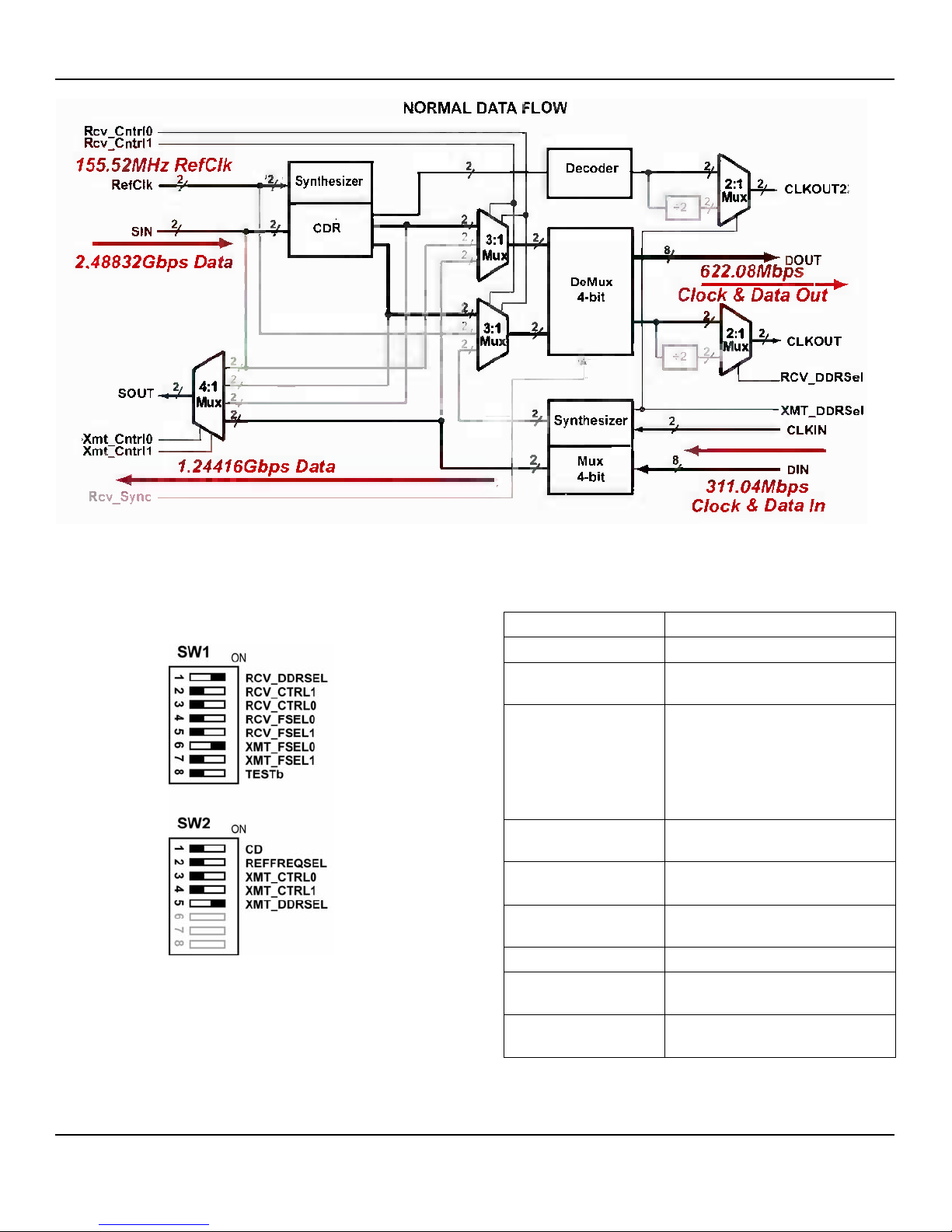
Normal Data Flow
This is the normal operating mode and verifies the receive
and transmit sections independently, which means any
combination of the allowed receive and transmit data
rates can be used. The switch settings below select the
frequencies and data rates specified in the block diagram.
Figure 6. Switch Settings for Normal Data Flow
Switch Settings
Function
RCV_DDRSEL = 0
Sets Clkout at parallel data rate
RCV_CTRL0/1 = 11
Selects the normal receive data
path
RCV_FSEL0/1 = 11
Sets receive CDR frequency to
2.48832Gbps (For other
frequencies, refer to Receive
Frequency Selection Table on
page 7 of SY87725L Data
sheet.)
XMT_FSEL0/1 = 01
Sets parallel data rate to be
1.24416Gbps/4
TESTb = 1
Disables factory test mode
(enables normal operation)
CD = 1
Enables clock and data
recovery
REFFREQSEL = 1
Selects RefClk of 155.52MHz
XMT_CTRL0/1 = 11
Selects the normal transmit
data path
XMT_DDRSEL = 1
Selects Clkin to be at parallel
data rate
Table 7. Required Switch Settings for
Normal Data Flow
Micrel, Inc.
SY87725L Evaluation Board
July 2008
11
M9999-071108-B
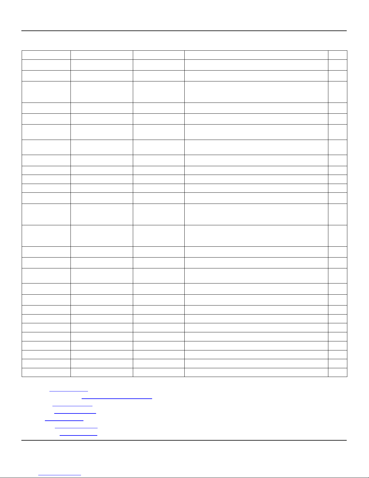
BiIl of Materials
Item
Part Number
Manufacturer
Description
Qty
C1-C3
VJ0603Y104JXJAT
Vishay
(1)
0.1mF, ceramic capacitor, size 0603
3
C4-C6
VJ1206Y106JXJAT
Vishay
(1)
10 mF, ceramic capacitor, size 1206
3
C7-C36, C38C42, C45-C51,
C56-C57
VJ0402Y104JXJAT
Vishay
(1)
0.1mF, ceramic capacitor, size 0402
43
C43-C45, C55
VJ0603Y105JXJAT
Vishay
(1)
1.0mF, ceramic capacitor, size 0603
4
C52-C54
VJ0402Y103JXJAT
Vishay
(1)
0.01mF, ceramic capacitor, size 0402
3
J3-J6, J32-J34
142-0711-821
Johnson
Components
(2)
SMA End Launch Receptacle connector
8
J7-J34
142-0711-201
Johnson
Components
(2
SMA Connector. Strait Jack Receptacle. Surface Mount.
28
L1-L4
IMC0805RK122J01
Vishay
(1)
1.2mH Ferrite bead inductor
4
D1
67-1640-1-ND
Digikey
(3)
Green LED
1
D2
67-1636-1-ND
Digikey
(3)
Red LED
1
Q1-Q3
MMBT3904WT1
ON Semi
(4)
General purpose NPN transistor
3
C37
CRCW040200R0F
Vishay
(1)
0W resistor, size 0402
1
R1-R2, R15,
R17, R19, R27,
R29, R72
CRCW04021270F
Vishay
(1)
127W, 1% resistor, size 0402
8
R3-R4, R16,
R18, R20, R28,
R30-R31
CRCW040282R5F
Vishay
(1)
82.5W resistor, size 0402
8
R9, R11
CRCW04021002F
Vishay
(1)
1.2kW, 5% resistor, size 0402
2
R10
CRCW04021002F
Vishay
(1)
390W, 5% resistor, size 0402
5
R12-R14, R32,
R47-R48
CRCW04021820F
Vishay
(1)
182W, 1% resistor, size 0402
6
R33-R46
CRCW04025111F
Vishay
(1)
5.11kW, 5% resistor, size 0402
14
R49-R53
CRCW04021002F
Vishay
(1)
10kW, 5% resistor, size 0402
5
SW1-SW2
TDA08H0SB1
C&K
(5)
DIP Switch, SMT
2
TP3
5010K-ND
Digikey
(3)
PC Test point Multi-purpose, Red
1
TP4
5011K-ND
Digikey
(3)
PC Test point Multi-purpose, Black
1
U1
SY87725L
Micrel
(7)
2.5Gbps GPON/APON ONU SERDES
1
U2
SY89322V
Micrel
(7)
Dual LVTTL-to-Differential LVPECL Translator
1
U3
SY89312V
Micrel
(7)
LVPECL ÷ 2 Clock Divider
1
U4
M210024BPN
MtronPTI
(6)
155.52MHz Clock Oscillator
1
PCB
SY87725_EB_R0
Micrel
(7)
Bare PCB
1
Notes:
1. Vishay: www.vishay.com
2. Johnson Components: www.johnsoncomponents.com.
3. Digi-key: www.digikey.com
4. On-Semi: www.on-semi.com
5. C&K: www.vishay.com
6. MtronPTI: www.mtronpti.com
7. Micrel, Inc.: www.micrel.com.

Micrel, Inc.
SY87725L Evaluation Board
July 2008
12
M9999-071108-B
APPENDIX
TEST FLOW DIAGRAM FOR SY87725L EVALUATION BOARD

Micrel, Inc.
SY87725L Evaluation Board
July 2008
13
M9999-071108-B
APPENDIX
TEST FLOW DIAGRAM FOR SY87725L CONTINUED

Micrel, Inc.
SY87725L Evaluation Board
July 2008
14
M9999-071108-B
HBW Support
Hotline: 408-955-1690
Email Support: HBWHelp@micrel.com
Application Hints and Notes
For application notes on high speed termination on
PECL and LVPECL products, clock synthesizer
products, SONET jitter measurement, and other High
Bandwidth products go to Micrel’s website at:
http://www.micrel.com/. Once in Micrel’s website, follow
the steps below:
1. Click on “Product Info”.
2. In the Applications Information Box, choose
“Application Hints and Application Notes.”
MICREL, INC. 2180 FORTUNE DRIVE SAN JOSE, CA 95131 USA
TEL +1 (408) 944-0800 FAX +1 (408) 474-1000 WEB http://www.micrel.com
The information furnished by Micrel in this data sheet is believed to be accurate and reliable. However, no responsibility is assumed
by Micrel for its use. Micrel reserves the right to change circuitry and specifications at any time without notification to the customer.
Micrel Products are not designed or authorized for use as components in life support appliances, devices or systems where
malfunction of a product can reasonably be expected to result in personal injury. Life support devices or systems are devices or
systems that (a) are intended for surgical implant into the body or (b) support or sustain life, and whose failure to perform can be
reasonably expected to result in a significant injury to the user. A Purchaser’s use or sale of Micrel Products for use in life support
appliances, devices or systems is a Purchaser’s own risk and Purchaser agrees to fully indemnify Micrel for any damages
resulting from such use or sale.
© 2007 Micrel, Incorporated.
 Loading...