

MICREL SY69952A Datasheet

OC-3/STS-3
C
CLOCK RECOVERING
TRANSCEIVER
SY69952A
FEATURES
■ A complete SONET/SDH/ATM compatible single chip
Transmitter and Receiver
■ Seamless operation with PMC-Sierra PM5345, VLSI
VNS67200, Ig
µPD98402 UNI Processors
■ Supports clock and data recovery from 51.84 Mbit/s
or 155.52 Mbit/s NRZ or NRZI data stream
■ 155.52MHz clock multiplication from 19.44MHz
source or 51.84MHz clock multiplication from
6.48MHz source
■ Line Receiver Inputs: No external buffering needed
■ Differential output buffering
■ Link Status Indication
■ Loop-back testing
■ 100K ECL compatible I/O
■ Single +5 volt power supply
■ Available in 28-pin SOIC package
T WAC-013-B/WAC-413-A and
NEC
DESCRIPTION
Micrel-Synergy's SY69952A contains fully integrated
transmitter and receiver functions designed to provide
clock recovery and generation for either 51.84Mbit/s OC/
STS-1 or 155.52Mbit/s OC/STS-3 SONET/SDH
(SY69952) and ATM applications.
On-chip clock generation is performed by a low-jitter
phase-locked loop (PLL) allowing use of 19.44MHz
reference for 155.52MHz generation or a 6.48MHz
reference for 51.84MHz generation. Clock recovery is
performed by synchronizing the on-chip VCO directly to
the incoming data stream.
Micrel-Synergy's circuit design techniques coupled with
ASSET™ bipolar technology result in ultra-fast
performance with low noise and low power dissipation.
FUNCTIONAL BLOCK DIAGRAM
PLL2+
PLL2-
PLL
PLL
x8
PLL1+
PLL1-
RECEIVE
TRANSMIT
ROUT+
ROUT-
RIN+
RIN-
CD
TOUT+
TOUT-
LOOP MODE
REFCLK+
REFCLK-
RCLK+
RCLK-
RSER+
RSER-
LFI
TSER+
TSER-
TCLK+
TCLK-
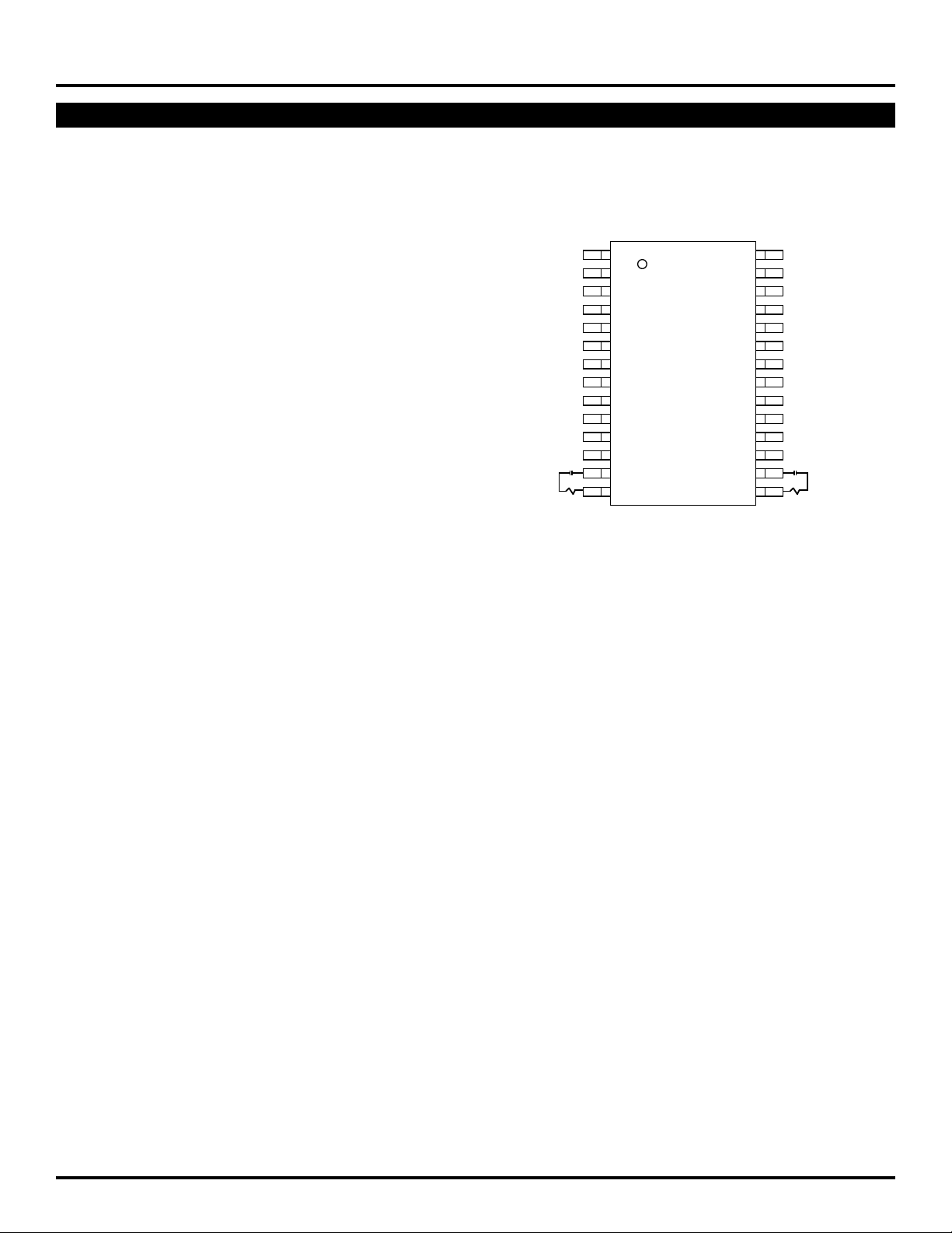
PIN CONFIGURATION
ROUT+
ROUT-
RIN+
RIN-
MODE
V
C
CD
LOOP
REFCLK-
REFCLK+
TOUT-
TOUT+
PLL1+
PLL1- PLL2-
1
2
3
4
5
6
7
8
9
10
11
12
13
14
TOP VIEW
SOIC
28
27
26
25
24
23
22
21
20
19
18
17
16
15
RCLKRCLK+
RSERRSER+
LFI
V
CC
V
EE
V
CC
TCLKTCLK+
TSER+
TSERPLL2+
Rev.: C Amendment: /0
1
Issue Date: May 2000

Micrel
PIN DESCRIPTIONS
SY69952A
INPUTS
± – Differential PECL Input
RIN
Receive Input. These built-in line receiver inputs are
connected to the differential Receive serial input data stream.
An internal Receive PLL recovers the embedded clock
(RCLK±) and data (RSER±) information. The incoming data
rate can be within one of two frequency ranges, mentioned
before depending on the state of the MODE pin.
CD – PECL/TTL Input
Carrier Detect. This input controls the recovery function
of the Receive PLL and can be driven by the carrier detect
output from optical modules or from external transition
detection circuitry. When this input is at an ECL HIGH, the
input data stream (RIN±) is recovered normally by the
Receive PLL. When this input is at an ECL LOW, the
Receive PLL no longer aligns to RIN±, but instead aligns
with the REFCLK × 8 frequency. Also, the Link Fault Indicator
(/LFI) will transition LOW, and the recovered data outputs
(RSER±) will remain LOW regardless of the signal level on
the Receive data stream inputs (RIN±). When the CD input
is at a TTL LOW (≤0.8V), the internal transition detection
circuitry is disabled. When in Loop-back testing mode,
regardless of the signal level on the CD input, the Receive
PLL is internally turned-on to allow data stream transmission
to the recovered serial data outputs (RSER±) from the
Transmit serial data inputs (TSER±).
TSER
± – Differential PECL Input
Transmit Serial Data. These built-in line receiver inputs
are connected to the differential Transmit serial input data
stream. These inputs can receive very low amplitude signals
and are compatible with PECL signal levels.
REFCLK± – Differential PECL/TTL Input
Reference Clock. This input is the clock frequency
reference for the clock and data recovery Receive PLL.
REFCLK is multiplied internally by eight and sets the
approximate center frequency for the internal Receive PLL
to track the incoming bit stream. This input is also multiplied
by eight by the frequency multiplier Transmit PLL to produce
the bit rate Transmit Clock (TCLK±). REFCLK can be
connected to either a differential PECL or single-ended TTL
frequency source. When either REFCLK+ or REFCLK- is at
a TTL LOW, the opposite REFCLK signal becomes a TTL
level input.
OUTPUTS
ROUT± – Differential PECL Output
Receive Output. These Positive ECL 100K outputs (+5V
referenced) represent the buffered version of the input data
stream (RIN±). This output pair can be used for Receiver
input data equalization in copper based systems, reducing
the system impact of data dependent jitter. All PECL outputs
can be powered down by connecting both outputs to VCC
or leaving them both unconnected.
± – Differential PECL Output
RSER
Recovered Serial Data. These Positive ECL 100K outputs
(+5V referenced) represent the recovered data from the
input data stream (RIN±). This recovered data is aligned
with the recovered clock (RCLK±) with a sampling window
compatible with most data processing devices.
RCLK± – Differential PECL Output
Recovered Clock. These Positive ECL 100K outputs (+5V
referenced) represent the recovered clock from the input
data stream (RIN±). This recovered clock is used to sample
the recovered data (RSER±) and has timing compatible
with most data processing devices.
/LFI – TTL Output
Link Fault Indicator. This output indicates the status of
the input data stream (RIN±). It is controlled by three
functions; the Carrier Detect (CD) input, the internal
Transition Detector, and the Out of Lock (OOL) detector.
The Transition Detector determines if RIN± contains enough
transitions to be accurately recovered by the Receive PLL.
The Out of Lock detector determines if RIN± is within the
frequency range of the Receive PLL. When CD is HIGH
and RIN± has sufficient transitions and is within the
frequency range of the Receive PLL, the /LFI output will be
high. If CD is at an ECL LOW or RIN± does not contain
sufficient transitions or RIN± is outside the frequency range
of the Receive PLL then the /LFI output will be LOW. If CD
is at a TTL LOW then the /LFI output will only transition
LOW when the frequency of RIN± is outside the range of
the Receive PLL.
TOUT
± – Differential PECL Output
Transmit Output. These Positive ECL 100K outputs (+5V
referenced) represent the buffered version of the Transmit
data stream (TSER±). This Transmit path is used to take
weak input signals and rebuffer them to drive low impedance
copper media.
TCLK± – Differential PECL Output
Transmit Clock. These Positive ECL 100K outputs (+5V
referenced) provide the bit rate frequency source for external
Transmit data processing devices. This output is synthesized
by the Transmit PLL and is derived by multiplying the
REFCLK frequency by eight.
2
Micrel
Transmit
Filter
PIN DESCRIPTIONS
SY69952A
/LOOP – TTL Input
Loop Back Select. This input is used to select the input
data stream source that the Receive PLL uses for clock
and data recovery. When the /LOOP input is HIGH, the
Receive input data stream (RIN±) is used for clock and
data recovery. When /LOOP is LOW, the Transmit input
data stream (TSER±) is used by the Receive PLL for clock
and data recovery. When in Loop-back testing mode, /LOOP
input asserted low, the Receive PLL is always turned-on
internally regardless of the CD input signal level status.
This allows the Recovered Serial Data outputs (RSER±) to
receive data stream from the Transmit serial data inputs
(TSER±).
MODE – 3 Level Input
Frequency Mode Select. This three-level input selects
the frequency range for the clock and data recovery receive
PLL and the frequency multiplier transmit PLL. When the
input is held PECL HIGH (VCC –0.9 typ.), the two PLLs
operate at the SONET (SDH) STS-3 (STM-1) line rate of
155.52MHz. When this input is held TTL LOW (connected
to GND), the two PLLs operate at one SONET STS-1 line
rate of 51.84MHz. The REFCLK± frequency in both operating
modes is 1⁄8 of the operating frequency. When the MODE
input is ECL LOW (VCC – 1.7 typ), the device enters into
test mode, the TSER± inputs substitue for the internal PLL
VCO for use in factory testing.
PLL1±, PLL2± – Loop Filter Inputs
These pins are used to connect the external loop filters
for the two on-board PLLs. See below:
TOP VIEW
0.1µf
500Ω
Figure 1. Suggested Loop Filter Values
PLL1+
PLL1- PLL2-
PLL2+
0.1µf
120Ω
Receiver
Filter
3
 Loading...