

MICREL SY10H641L, SY100H641L Datasheet
3.3V SINGLE SUPPLY
1:9 PECL-TO-TTL
ClockWorks™
PRELIMINARY
SY10H641L
SY100H641L
FEATURES
■ 3.3V power supply
■ PECL-to-TTL version of popular ECLinPS E111
■ Guaranteed low skew specification
■ Latched input
■ Differential ECL internal design
■ V
BB output for single-ended operation
■ Reset/enable
■ Extra TTL and ECL power/ground pins
■ Choice of ECL compatibility: MECL 10KH (10Hxxx)
or 100K (100Hxxx)
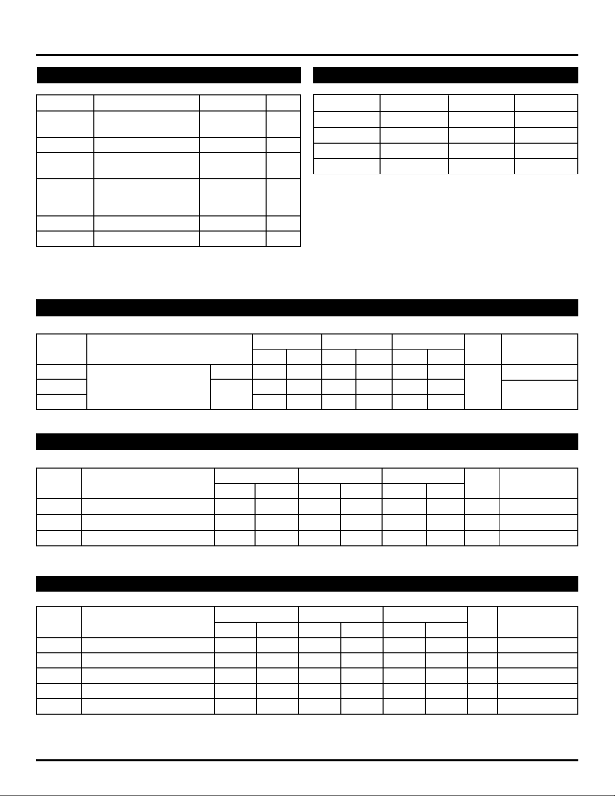
■ Available in 28-pin PLCC package
TTL Outputs
Q
0
Q
1
Q
2
DESCRIPTION
The SY10/100H641L are single supply, low skew
translating 1:9 clock drivers. Devices in the MicrelSynergy H600 translator series utilize the 28-lead PLCC
for optimal power pinning, signal flow-through and
electrical performance.
The devices feature a 24mA TTL output stage with
AC performance specified into a 20pF load capacitance.
A latch is provided on-chip. When LEN is LOW (or left
open, in which case it is pulled LOW by the internal pulldowns), the latch is transparent. A HIGH on the enable
pin (/EN) forces all outputs LOW.
The 10H version is compatible with MECL 10KH ECL
logic levels. The 100H version is compatible with 100K
levels.
PIN CONFIGURATIONBLOCK DIAGRAM
7
6
T
T
V
Q
G
25
24 23 22 21 20 19
G
Q
Q
Q
G
26
T
27
5
28
V
T
1
4
2
V
T
3
3
4
T
TOP VIEW
PLCC
567891011
8
T
T
V
Q
Q
G
18
V
BB
17
D
16
D
15
V
E
14
LEN
13
G
E
12
EN
PECL Input
D
D
V
BB
LEN
EN
DQ
Q
3
Q
4
PIN NAMES
2
1
0
T
T
T
V
Q
G
Q
T
V
Q
G
Pin Function
Q
5
GT TTL Ground (0V)
VT TTL VCC (+3.0V)
Q
6
VE ECL VCC (+3.0V)
GE ECL Ground (0V)
D, /D Signal Input (PECL)
Q
7
VBB VBB Reference Output (PECL)
Q0 – Q8 Signal Outputs (TTL)
/EN Enable Input (PECL)
Q
8
LEN Latch Enable Input (PECL)
1
Rev.: D Amendment: /0
Issue Date: May 2000
Micrel
ClockWorks™
PRELIMINARY
SY10H641L
SY100H641L
ABSOLUTE MAXIMUM RATINGS
(1)
Symbol Rating Value Unit
E (ECL) Power Supply –0.5 to +7.0 V
V
VT (TTL) Voltage –0.5 to +7.0
VI (ECL) Input Voltage 0.0 to VE V
V
OUT (TTL) Disabled 3-State 0.0 to VT V
Output
I
OUT (ECL) Output Current mA
TRUTH TABLE
D LEN /EN Q
LL LL
HL LH
XH LQ0
XX HL
- Continuous 50
- Surge 100
Tstore Storage Temperature –65 to +150 °C
T
A Operating Temperature 0 to +85 °C
NOTE:
1. Do not exceed.
DC ELECTRICAL CHARACTERISTICS
VT = VE = +3.0V to +3.6V
TA = 0°CTA = +25°CTA = +85°C
Symbol Parameter Min. Max. Min. Max. Min. Max. Unit Condition
EE Power Supply Current ECL — 30 — 30 — 30 mA VE Pin
I
CCH TTL — 30 — 30 — 30 Total all VT pins
I
CCL —35 —35 — 35
I
TTL DC ELECTRICAL CHARACTERISTICS
VT = VE = +3.0V to +3.6V
TA = 0°CTA = +25°CTA = +85°C
Symbol Parameter Min. Max. Min. Max. Min. Max. Unit Condition
VOH Output HIGH Voltage 2.0 — 2.0 — 2.0 — V IOH = –3.0mA
VOL Output LOW Voltage — 0.5 — 0.5 — 0.5 V IOL = 24mA
OS Output Short Circuit Current –100 — –100 — –100 — mA VOUT = 0V
I
10H ECL DC ELECTRICAL CHARACTERISTICS
VT = VE = +3.0V to +3.6V
TA = 0°CTA = +25°CTA = +85°C
Symbol Parameter Min. Max. Min. Max. Min. Max. Unit Condition
IIH Input HIGH Current — 225 — 175 — 175 µA—
IIL Input LOW Current 0.5 — 0.5 — 0.5 — µA—
(1)
(1)
(1)
2.130 2.460 2.170 2.490 2.240 2.580 V VE = 3.3V
1.350 1.820 1.350 1.820 1.350 1.855 V VE = 3.3V
1.920 2.030 1.950 2.050 1.990 2.110 V VE = 3.3V
VIH Input HIGH Voltage
VIL Input LOW Voltage
VBB Output Reference Voltage
NOTE:
1. VIH, VIL and VBB are referenced to VE and will vary 1:1 with the power supply. The levels shown are for VE = +3.3V.
2
 Loading...