

MICREL SY10H602, SY100H602 Datasheet
9-BIT LATCHED
0
L
2
3
4
5
6
7
8
TTL-TO-ECL
SY10H602
SY100H602
FEATURES
■ 9-bit ideal for byte-parity applications
■ Flow-through configuration
■ Extra TTL and ECL power/ground pins to minimize
switching noise
■ Dual supply
■ 3.5ns max. D to Q
■ PNP TTL inputs for low loading
■ Choice of ECL compatibility: MECL 10KH (10Hxxx)
or 100K (100Hxxx)
■ Fully compatible with Motorola MC10H/100H602
■ Available in 28-pin PLCC package
DESCRIPTION
The SY10/100H602 are 9-bit, dual supply TTL-to-ECL
translators with latches. Devices in the Micrel-Synergy
9-bit translator series utilize the 28-lead PLCC for optimal
power pinning, signal flow-through and electrical
performance.
The H602 features D-type latches. Latching is
controlled by Latch Enable (LEN), while the Master Reset
input resets the latches. A post-latch logic enable is also
provided (ENECL), allowing control of the output state
without destroying latch data. All control inputs are ECL
level.
The 10H version is compatible with MECL 10KH ECL
logic levels. The 100H version is compatible with 100K
levels.
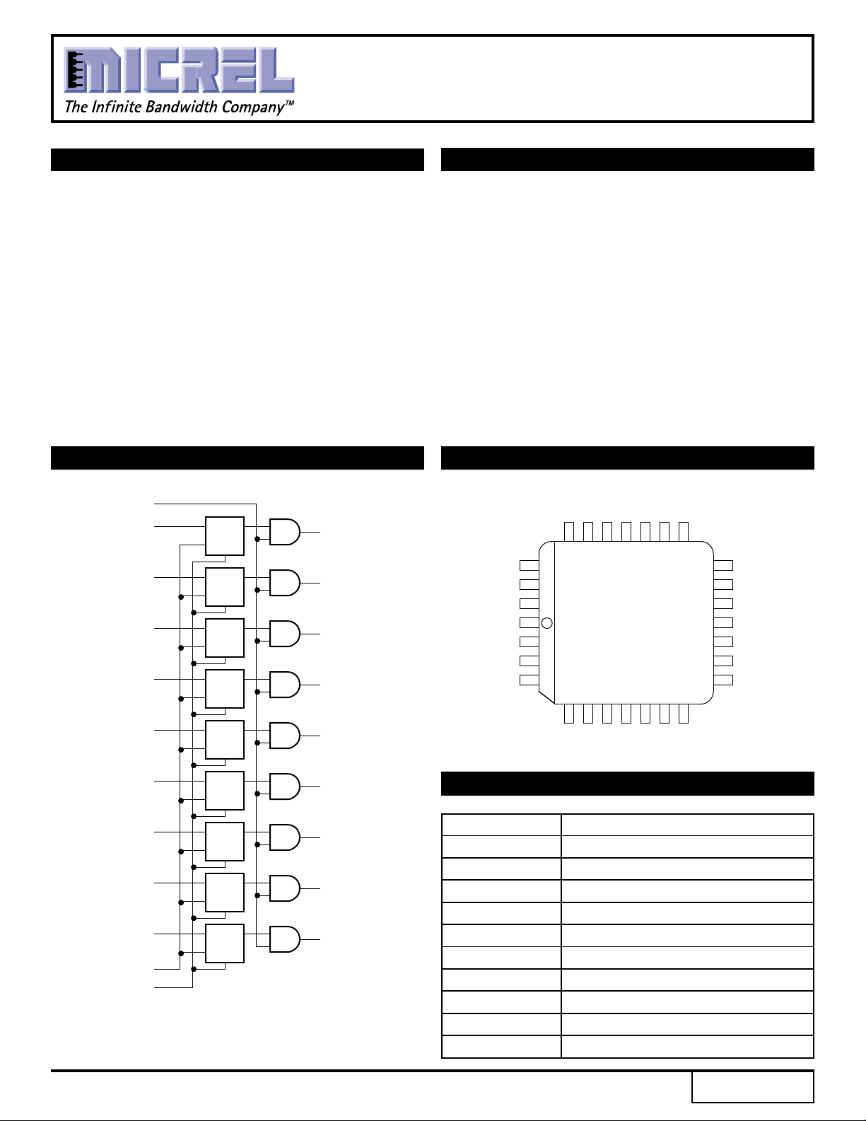
BLOCK DIAGRAM PIN CONFIGURATION
ENECL
D
D1 QD
D
D
EN
EN
EN
EN
QD
Q0
D6
Q1
D7
D8
QD
Q2
GND
MR
LEN
QD
Q3
ENECL
D5
25 24 23 22 21 20 19
26
27
28
1
2
3
4
567891011
D4
VCCTD3D2
TOP VIEW
PLCC
D1
D0
18
Q
0
17
Q1
16
VCCE
15
VCCO
14
Q2
13
VCCO
12
Q3
TT
D
D
D
EN
EN
EN
QD
QD
QD
Q4
Q5
Q6
ECL
Q7
Q6
Q8
VCCO
VEE
Q5
PIN NAMES
Pin Function
GND TTL Ground (0V)
Q4
VCCE ECL VCC (0V)
D
EN
QD
Q7
VCCO ECL VCC (0V) — Outputs
VCCT TTL Supply (+5.0V)
D
LEN
MR
EN
QD
Q8
VEE ECL Supply (–5.2/–4.5V)
D0–D8 Data Inputs (TTL)
Q0–Q8 Data Outputs (ECL)
ENECL Enable Control (ECL)
LEN Latch Enable (ECL)
MR Master Reset (ECL)
Rev.: D Amendment: /0
1
Issue Date: March, 1998

Micrel
SY100H602
LOGIC DIAGRAMTRUTH TABLE
D LEN MR ENECL Q
LLLHL
HLLHH
XHLHQ0
XXHHL
XXXLL
DC ELECTRICAL CHARACTERISTICS
VCCT = 5.0V ± 10%; VEE = –4.75V to –5.5V (10H Version); VEE = –4.2V to –5.5V (100H Version)
TA = 0°CTA = +25°CTA = +85°C
Symbol Parameter Min. Max. Min. Max. Min. Max. Unit Condition
EE Power Supply Current, ECL mA —
I
10H — 125 — 125 — 125
100H — 122 — 123 — 132
ICCH Power Supply Current, TTL — 48 — 48 — 48 mA —
ICCL — 50 — 50 — 50
SY10H602
AC ELECTRICAL CHARACTERISTICS
LOGIC DIAGRAM
VCCT = 5.0V ± 10%; VEE = –4.75V to –5.5V (10H Version); VEE = –4.2V to –5.5V (100H Version)
TA = 0°CTA = +25°CTA = +85°C
Symbol Parameter Min. Max. Min. Max. Min. Max. Unit Condition
tPLH Propagation Delay to Output ns —
tPHL D 1.4 3.0 1.5 3.2 1.7 3.5
LEN 2.0 3.4 2.1 3.5 2.4 3.7
MR 2.0 3.4 2.1 3.5 2.5 3.9
ENECL 1.6 3.2 1.7 3.3 1.8 3.7
tS Set-up Time, D to LEN 2.0 — 2.0 — 2.0 — ns —
tH Hold Time, D to LEN 1.0 — 1.0 — 1.0 — ns —
(L)
tw
t
r Output Rise/Fall Time 0.5 1.5 0.5 1.5 0.5 1.5 ns —
tf 20% to 80%, 80% to 20%
LEN Pulse Width, LOW 2.0 — 2.0 — 2.0 — ns —
PRODUCT ORDERING CODE
Ordering Package Operating
Code Type Range
SY10H602JC J28-1 Commercial
SY10H602JCTR J28-1 Commercial
SY100H602JC J28-1 Commercial
SY100H602JCTR J28-1 Commercial
2
 Loading...