

MICREL SY10EP58VZC, SY10EP58VKC, SY10EP58VKCTR Datasheet
5V/3.3V
2:1 MULTIPLEXER
PRELIMINARY
SY10EP58V
FEATURES
■ 3.3V and 5V power supply options
■ 275ps typical propagation delay
■ High bandwidth to XGHz min.
■ 75kΩ internal input pulldown resistors
■ Q output will default LOW with inputs open or at V
■ Available in 8-pin SOIC and 10-pin MSOP packages
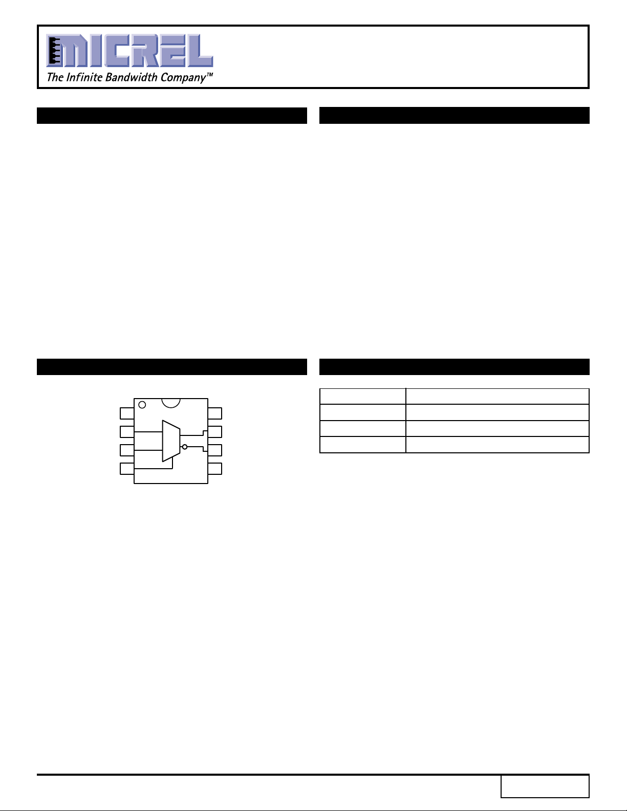
PIN CONFIGURATION/BLOCK DIAGRAM
Da
Db
1NC
2
3
1
MUX
0
8 VCC
Q
7
/Q
6
DESCRIPTION
The SY10EP58V is a 2:1 multiplexer. The device is
pin and functionally equivalent to the SY100EL58 device.
EE
PIN NAMES
Pin Function
Da, Db ECL Data Inputs
SEL ECL Select Inputs
Q, /Q ECL Data Outputs
SEL
4
Available in 8-Pin SOIC or MSOP package
VEE
5
1
Rev.: A Amendment: /1
Issue Date:
December 2000
Micrel
SY10EP58V
ABSOLUTE MAXIMUM RATINGS
(1)
Symbol Rating Value Unit
V
CC
V
EE
V
I
V
I
I
OUT
T
A
T
store
NOTE:
1. Permanent device damage may occur if ABSOLUTE MAXIMUM RATINGS are exceeded. This is a stress rating only and functional operation is not implied
at conditions other than those detailed in the operational sections of this data sheet. Exposure to ABSOLUTE MAXIMUM RATlNG conditions for extended
periods may affect device reliability.
DC ELECTRICAL CHARACTERISTICS
VCC = 0V; VEE = –5.5V to –3.0V or VCC = +3.3V ±10%; VEE = 0V or VCC = +5.0V ±10%, VEE = 0V
Power Supply Voltage (VEE = 0) –6.0 to 0 Vdc
Power Supply Voltage (VCC = 0) +6.0 to 0 Vdc
Input Voltage (VCC = 0V) –6.0 to 0 Vdc
Input Voltage (VEE = 0V) +6.0 to 0 Vdc
Output Current –Continuous 50 mA
–Surge 100
Operating Temperature Range –40 to +85 °C
Storage Temperature Range –65 to +150 °C
(1)
(4)
TA = –40°CT
= +25°CT
A
= +85°C
A
Symbol Parameter Min. Max. Min. Typ. Max. Min. Max. Unit
(3)
(2)
(3)
20 40 20 30 40 22 40 mA
VCC –1135 VCC –885 VCC –1070 VCC –945 VCC –820 VCC –1010 VCC –760 mV
VCC –1935 VCC –1685 VCC –1870 VCC –1745 VCC –1620 VCC –1810 VCC –1560 mV
I
EE
V
OH
V
OL
V
IH
V
IL
I
IH
I
IL
NOTES:
1. 10EP circuits are designed to meet the DC specifications shown in the above table after thermal equilibrium has been established. The circuit
is in a test socket or mounted on a printed circuit board and traverse airflow greater than 500lfpm is maintained.
2. VCC = 0V, VEE = –3.3V, all other pins floating.
3. All loading with 50Ω to VCC –3.0V.
4. Input and output parameters vary 1:1 with VCC.
Power Supply Current
Output HIGH Voltage
Outuput LOW Voltage
Input HIGH Voltage VCC –1210 VCC –885 VCC –1145 — VCC –820 VCC –1085 VCC –760 mV
Input LOW Voltage VCC –1935 VCC –1610 VCC –1870 — VCC –1545 VCC –1810 VCC –1485 mV
Input HIGH Current — 150 — — 150 — 150 µA
Input LOW Current D 0.5 — 0.5 — — 0.5 — µA
2
 Loading...