

MICREL SY10E431, SY100E431 Datasheet
3-BIT DIFFERENTIAL
FLIP-FLOP
SY10E431
SY100E431
FEATURES
■ Differential D, clock and Q
■ Extended 100E VEE range of –4.2V to –5.5V
■ VBB output for single-ended use
■ 1100MHz min. toggle frequency
■ Edge-triggered asynchronous set and reset
■ Fully compatible with Motorola MC10E/100E431
■ Available in 28-pin PLCC package
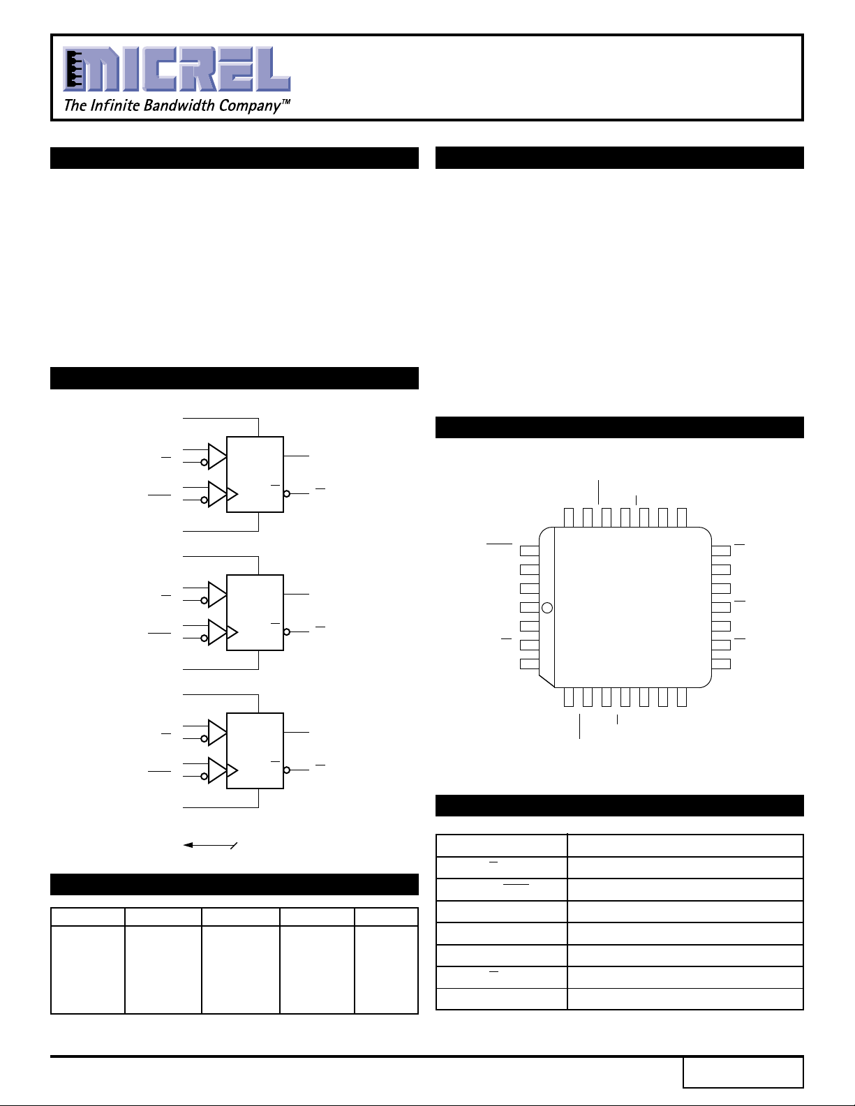
BLOCK DIAGRAM
S
0
S
DQ
Q
R
S
DQ
Q
R
Q
0
Q
0
Q
1
Q
1
CLK
CLK
CLK
CLK
D
0
D
0
0
0
R
0
S
1
D
1
D
1
1
1
R
1
S
2
DESCRIPTION
The SY10/100E431 are 3-bit flip-flops with differential
clock, data input and data output.
The asynchronous Set and Reset controls are edgetriggered rather than level controlled. This allows the user
to rapidly set or reset the flip-flop and then continue
clocking at the next clock edge without the necessity of
de-asserting the set/reset signal (as would be the case
with a level controlled set/reset).
The E431 is also designed with larger internal swings,
an approach intended to minimize the time spent crossing
the threshold region and thus reduces the metastability
susceptibility window.
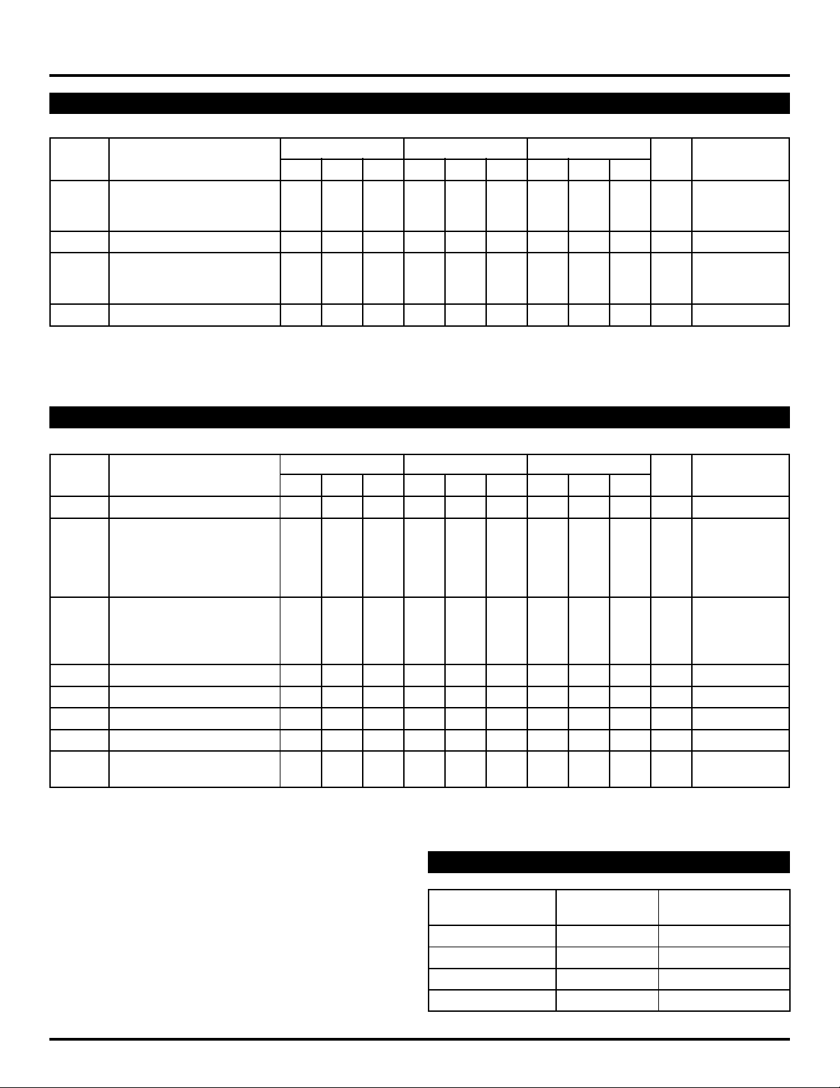
PIN CONFIGURATION
VBB
CLK2
D2
CLK1
CLK1
R1
VEE
S1
D1
D1
CLK2
25
24 23 22 21 20 19
26
27
28
1
2
3
4
TOP VIEW
PLCC
J28-1
567891011
R2
S2
D2
18
Q2
17
Q2
16
VCC
15
Q1
14
Q1
13
Q0
12
Q0
D
D
CLK
CLK
R
V
BB
TRUTH TABLE
2
2
2
2
2
(1)
S
DQ
Q
R
Q
2
Q
2
Dn CLKn Rn Sn Qn
LZ L L L
HZ L L H
XL Z L L
XL L Z H
NOTE:
1. Z = LOW-to-HIGH transition.
D0
D0
R0
CLK0
CLK0
S0
PIN NAMES
Pin Function
D[0:2], D[0:2] Differential Data Inputs
CLK[0:2], CLK[0:2] Differential Clock Inputs
S[0:2] Edge Triggered Set Inputs
R[0:2] Edge Triggered Reset Inputs
VBB VBB Reference Output
Q[0:2], Q[0:2] Differential Data Outputs
CCO VCC to Output
V
1
VCCO
Rev.: C Amendment: /1
Issue Date: February, 1998
SY10E431
Micrel
SY100E431
DC ELECTRICAL CHARACTERISTICS
VEE = VEE (Min.) to VEE (Max.); VCC = VCCO = GND
TA = 0°CTA = +25°CTA = +85°C
Symbol Parameter Min. Typ. Max. Min. Typ. Max. Min. Typ. Max. Unit Condition
BB Output Reference Voltage V—
V
10E –1.38 — –1.27 –1.35 — –1.25 –1.31 — –1.19
100E –1.38 — –1.26 –1.38 — –1.26 –1.38 — –1.26
IIH Input HIGH Current — — 150 — — 150 — — 150 µA—
EE Power Supply Current mA —
I
10E — 110 132 — 110 132 — 110 132
100E — 110 132 — 110 132 — 127 152
CMR Common Mode Range –1.5 — 0 –1.5 — 0 –1.5 — 0 V 1
V
NOTES:
CMR is referenced to the most positive side of the differential input signal. Normal operation is obtained when the input signals are within the VCMR range
1. V
and the input swing is greater than V
PP (min.) and <1V.
AC ELECTRICAL CHARACTERISTICS
VEE = VEE (Min.) to VEE (Max.); VCC = VCCO = GND
TA = 0°CTA = +25°CTA = +85°C
Symbol Parameter Min. Typ. Max. Min. Typ. Max. Min. Typ. Max. Unit Condition
fMAX Max. Toggle Frequency 1100 1400 — 1100 1400 — 1100 1400 — MHz —
PLH Propagation Delay to Output ps —
t
tPHL CLK (Diff) 450 600 750 450 600 750 450 600 750
CLK (SE) 400 600 800 400 600 800 400 600 800
R 550 725 925 550 725 925 550 725 925
S 550 725 925 550 725 925 550 725 925
t
S Set-up Time ps
D 200 0 — 200 0 — 200 0 —
R 1000 700 — 1000 700 — 1000 700 — 1
S 1000 700 — 1000 700 — 1000 700 — 1
tH Hold Time, D 200 0 — 200 0 — 200 0 — ps —
tPW Minimum Pulse Width, CLK 400 — — 400 — — 400 — — ps —
tskew Within-Device Skew — 50 — — 50 — — 50 — ps 2
VPP (AC) Minimum Input Swing 150 — — 150 — — 150 — — mV 3
r Rise/Fall Time 275 450 650 275 450 650 275 450 650 ps —
t
tf 20% to 80%
NOTES:
1. These set-up times define the minimum time the CLK or SET/RESET input
must wait after the assertion of the RESET/SET input to assure the proper
operation of the flip-flop.
2. Within-device skew is defined as identical transitions on similar paths
through a device.
3. Minimum input swing for which AC parameters are guaranteed.
PRODUCT ORDERING CODE
Ordering Package Operating
Code Type Range
SY10E431JC J28-1 Commercial
SY10E431JCTR J28-1 Commercial
SY100E431JC J28-1 Commercial
SY100E431JCTR J28-1 Commercial
2
 Loading...