

MICREL SY10E167, SY100E167 Datasheet
5-127
SY10E167
SY100E167
SY NERGY
SEMICONDUCTOR
© 1999 Micrel-Synergy
■ 1000MHz min. operating frequency
■ Extended 100E VEE range of –4.2V to –5.5V
■ 800ps max. clock to output
■ Single-ended outputs
■ Asynchronous Master Reset
■ Dual clocks
■ Fully compatible with industry standard 10KH,
100K ECL levels
■ Internal 75KΩ input pulldown resistors
■ ESD protection of 2000V
■ Fully compatible with Motorola MC10E/100E167
■ Available in 28-pin PLCC package
FEATURES
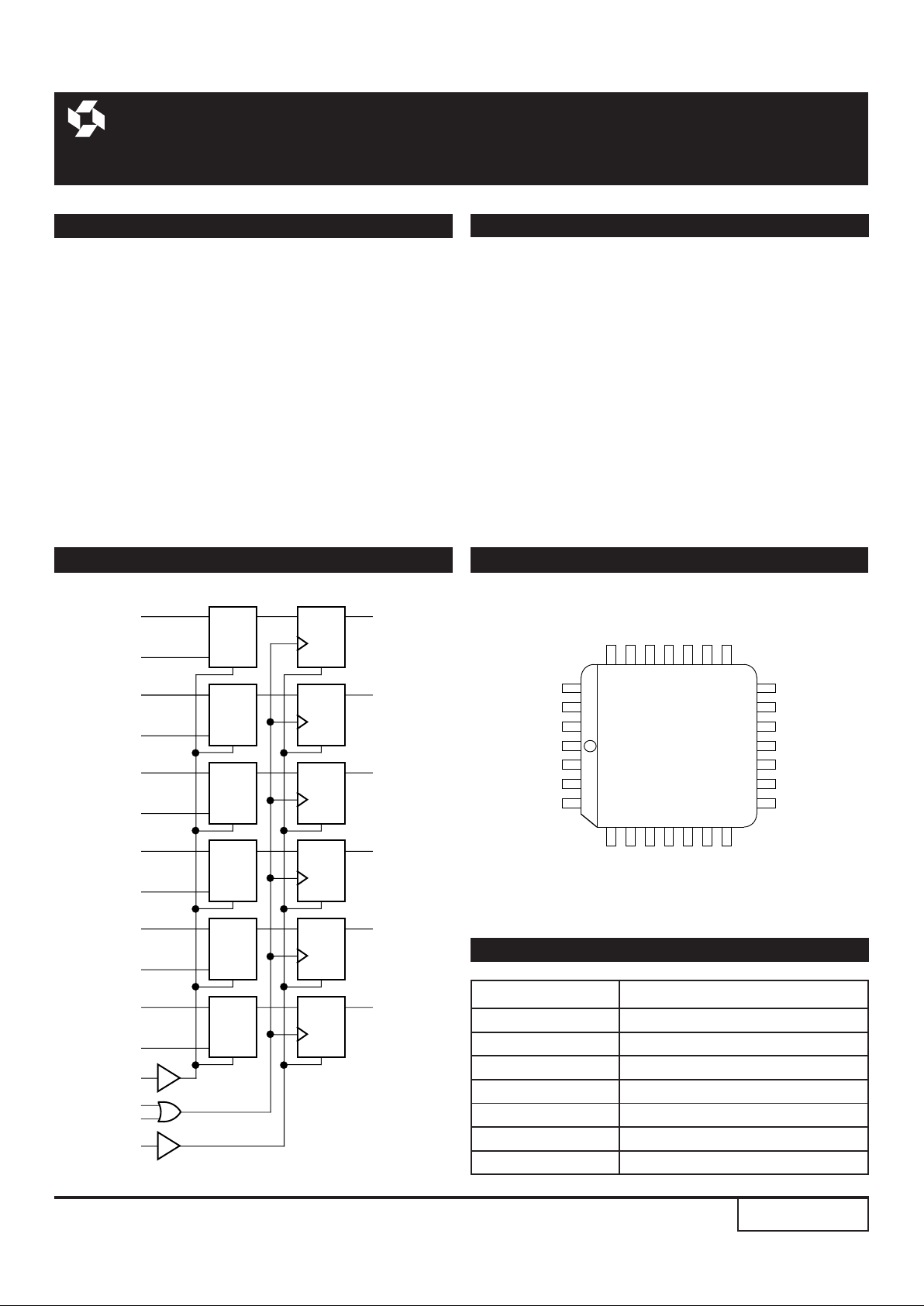
The SY10/100E167 offer six 2:1 multiplexers followed
by D flip-flops with single-ended outputs, designed for use
in new, high-performance ECL systems. The Select (SEL)
control allows one of the two data inputs to the multiplexer
to pass through. The two external clock signals (CLK1,
CLK2) are gated through a logical OR operation before use
as control for the six flip-flops. The selected data are
transferred to the flip-flops on the rising edge of CLK1 or
CLK2 (or both).
The multiplexer operation is controlled by the Select
(SEL) signal which selects one of the two bits of input data
at each mux to be passed through.
When a logic HIGH is applied to the Master Reset (MR)
signal, it operates asychronously to take all outputs Q to a
logic LOW.
DESCRIPTION
6-BIT 2:1 MUX-REGISTER
Rev.: C Amendment: /1
Issue Date: February, 1998
SY10E167
SY100E167
BLOCK DIAGRAM
PIN NAMES
Pin Function
D0a–D5a Input Data a
D0b–D5b Input Data b
SEL Select Input
CLK1, CLK2 Clock Inputs
MR Master Reset
Q0–Q5 Data Outputs
V
CCO VCC to Output
PIN CONFIGURATION
D
1b
V
CCO
Q
0
D
1a
D
0b
D
2a
D
2b
TOP VIEW
PLCC
J28-1
26
27
28
1
2
3
4
18
17
16
15
14
13
12
25 24 23 22 21 20 19
5 6 7 8 9 10 11
V
EE
D
5b
D
0a
MR
CLK
2
CLK
1
SEL
V
CC
Q
5
Q
4
Q
1
Q
3
Q
2
V
CCO
V
CCO
NC
D
3b
D
4a
D
4b
D
5a
D
3a
D
R
Q
MUX
SEL
D
R
Q
D
R
Q
D
R
Q
D
R
Q
D
R
Q
0
Q1
Q2
Q3
Q4
Q5
Q
MR
D
0a
CLK1
CLK2
SEL
D
0b
D1a
D1b
D2a
D2b
D3a
D3b
D4a
D4b
D5a
D5b
MUX
SEL
MUX
SEL
MUX
SEL
MUX
SEL
MUX
SEL
5-128
SY10E167
SY100E167
TRUTH TABLE
SEL Data
Ha
Lb
DC ELECTRICAL CHARACTERISTICS
AC ELECTRICAL CHARACTERISTICS
VEE = VEE (Min.) to VEE (Max.); VCC = VCCO = GND
TA = 0°CTA = +25°CTA = +85°C
Symbol Parameter Min. Typ. Max. Min. Typ. Max. Min. Typ. Max. Unit Condition
IIH Input HIGH Current — — 150 — — 150 — — 150 µA—
I
EE Power Supply Current mA —
10E — 94 113 — 94 113 — 94 113
100E — 94 113 — 94 113 — 108 130
VEE = VEE (Min.) to VEE (Max.); VCC = VCCO = GND
TA = 0°CTA = +25°CTA = +85°C
Symbol Parameter Min. Typ. Max. Min. Typ. Max. Min. Typ. Max. Unit Condition
fMAX Max. Toggle Frequency 1000 1400 — 1000 1400 — 1000 1400 — MHz —
t
PLH Propagation Delay to Output ps —
tPHL CLK 450 650 800 450 650 800 450 650 800
MR 450 650 850 450 650 850 450 650 850
t
S Set-up Time ps —
D 100 –50 — 100 –50 — 100 –50 —
SEL 275 125 — 275 125 — 275 125 —
t
H Hold Time ps —
D 300 50 — 300 50 — 300 50 —
SEL 75 –125 — 75 –125 — 75 –125 —
tRR Reset Recovery Time 750 550 — 750 550 — 750 550 — ps —
t
PW Minimum Pulse Width 400 — — 400 — — 400 — — ps —
CLK, MR
tskew Within-Device Skew — 75 — — 75 — — 75 — ps 1
t
r Rise/Fall Time 300 450 800 300 450 800 300 450 800 ps —
tf 20% to 80%
NOTE:
1. Within-device skew is defined as identical transitions on similar paths through a device.
PRODUCT ORDERING CODE
Ordering Package Operating
Code Type Range
SY10E167JC J28-1 Commercial
SY10E167JCTR J28-1 Commercial
SY100E167JC J28-1 Commercial
SY100E167JCTR J28-1 Commercial
SYNERGY
SEMICONDUCTOR
 Loading...