

MICREL SY10E141, SY100E141 Datasheet
8-BIT SHIFT
REGISTER
SY10E141
SY100E141
FEATURES
■ 700MHz min. shift frequency
■ Extended 100E VEE range of –4.2V to –5.5V
■ 8 bits wide
■ Bi-directional
■ Four selectable modes for full functionality
■ Asynchronous Master Reset
■ Fully compatible with industry standard 10KH,
100K ECL levels
■ Internal 75KΩ input pulldown resistors
■ Fully compatible with Motorola MC10E/100E141
■ Pin-compatible with E241
■ Available in 28-pin PLCC package
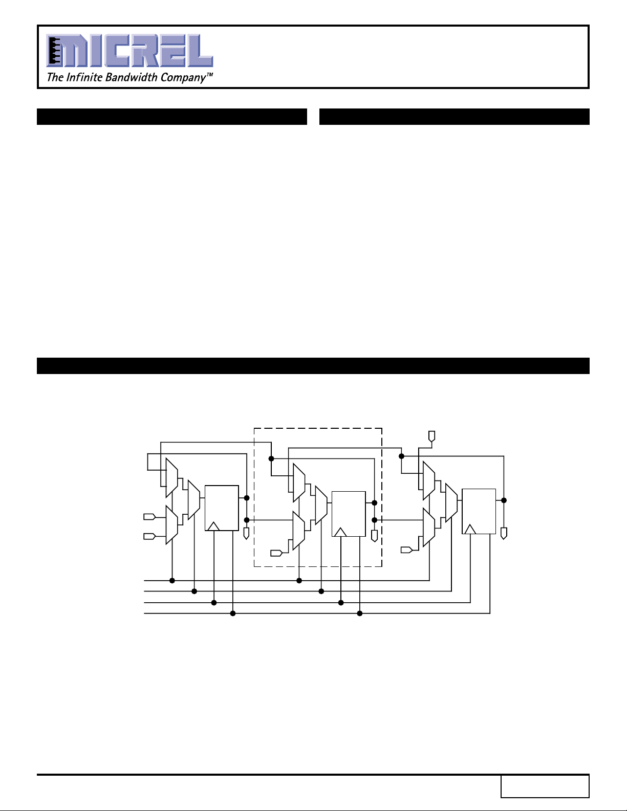
BLOCK DIAGRAM
DESCRIPTION
The SY10/100E141 are 8-bit, full-function shift registers
designed for use in new, high-performance ECL systems.
The E141 performs serial/parallel in and serial/parallel out,
shifting in either direction. The eight inputs D0–D7 accept
parallel input data, while DL/DR accept serial input data for
left/right shifting.
The two select pins, SEL0 and SEL1 permit four modes
of operation: Load, Hold, Shift Left and Shift Right, as
shown in the Truth Table. Input data is clocked into the
register on the rising clock edge after meeting the minimum
set-up time. A logic HIGH on the Master Reset (MR) pin
asynchronously resets all the registers to zero.
DR
D
0
SEL1
SEL0
CLK
MR
DQ
R
DL
BITS 1-6
Q
DQ
R
Q
0
D
Q
D
7
D
R
Q
7
Rev.: C Amendment: /1
1
Issue Date: February, 1998
Micrel
SY10E141
SY100E141
PIN CONFIGURATION
0
7
SEL
DL
25 24 23 22 21 20 19
SEL
1
26
CLK
MR
V
DR
EE
D
D
27
28
1
2
0
3
1
4
567891011
3
2
D
D
PLCC
TOP VIEW
J28-1
4
D
TRUTH TABLE
D6D
CCO
V
PIN NAMES
7
5
CCO
Q
V
D
18
Q
6
17
Q
5
16
V
CC
NC
15
14
13
12
1
0
2
Q
Q
Q
V
Q
Q
CCO
4
3
Pin Function
D0-D7 Parallel Data Inputs
DL, DR Serial Data Inputs
SEL0, SEL1 Mode Select Inputs
CLK Clock
Q0-Q7 Data Outputs
MR Master Reset
V
CCO VCC to Output
Function DL DR SEL0 SEL1 MR CLK Q0 Q1 Q2 Q3 Q4 Q5 Q6 Q7
Load X X L L L Z D0 D1 D2 D3 D4 D5 D6 D7
Shift Right X L L H L Z L Q0 Q1 Q2 Q3 Q4 Q5 Q6
XHLHLZ HLQ0 Q1 Q2 Q3 Q4 Q5
Shift Left L X H L L Z L Q0 Q1 Q2 Q3 Q4 Q5 L
HXHLLZQ0 Q1 Q2 Q3 Q4 Q5 LH
Hold X X H H L Z Q
0 Q1 Q2 Q3 Q4 Q5 LH
XXHHLZQ0 Q1 Q2 Q3 Q4 Q5 LH
Reset XXXXHX LLLLLLLL
DC ELECTRICAL CHARACTERISTICS
VEE = VEE (Min.) to VEE (Max.); VCC = VCCO = GND
TA = 0°CTA = +25°CTA = +85°C
Symbol Parameter Min. Typ. Max. Min. Typ. Max. Min. Typ. Max. Unit Condition
IIH Input HIGH Current ——150 ——150 ——150 µA —
EE Power Supply Current mA —
I
10E — 131 157 — 131 157 — 131 157
100E — 131 157 — 131 157 — 151 181
2
 Loading...