

MICREL SY10E111, SY100E111 Datasheet
1:9 DIFFERENTIAL CLOCK
DRIVER WITH ENABLE
ClockWorks™
SY10E111
SY100E111
FEATURES
■ Low skew
■ Extended 100E VEE range of –4.2V to –5.5V
■ Guaranteed skew limits
■ Differential design
■ VBB output
■ Enable input
■ Fully compatible with industry standard 10KH, 100K
I/O levels
■ 75KΩ input pulldown resistors
■ Fully compatible with Motorola MC10E/100E111
■ Available in 28-pin PLCC package
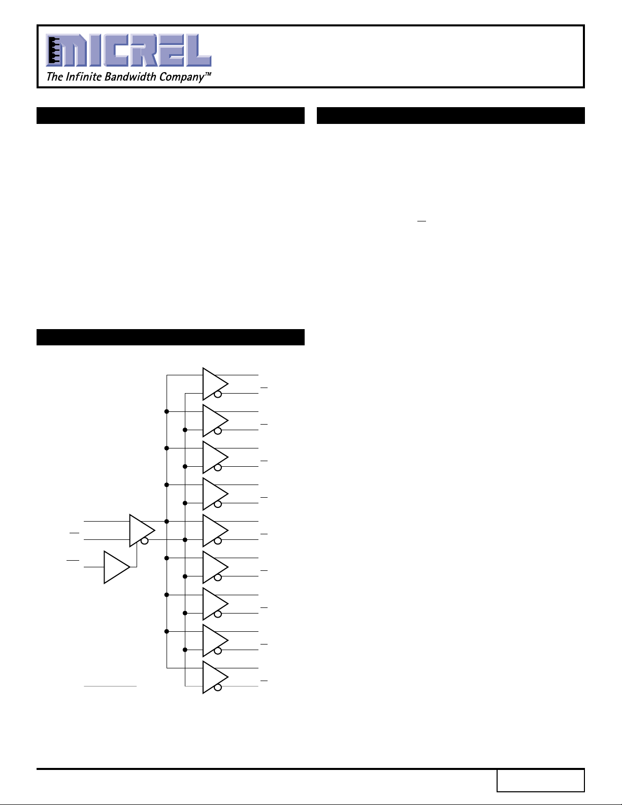
BLOCK DIAGRAM
Q0
Q0
Q1
Q1
Q2
Q2
Q3
Q3
IN
Q4
DESCRIPTION
The SY10/100E111 are low skew 1-to-9 differential
drivers designed for clock distribution in new, highperformance ECL systems. They accept one differential or
single-ended input, with VBB used for single-ended
operation. The signal is fanned out to nine identical
differential outputs. An enable input is also provided such
that a logic HIGH disables the device by forcing all Q
outputs LOW and all Q outputs HIGH.
The device is specifically designed and produced for low
skew. The interconnect scheme and metal layout are
carefully optimized for minimal gate-to-gate skew within
the device. Wafer characterization and process control
ensure consistent distribution of propagation delay from lot
to lot. Since the E111 shares a common set of “basic”
processing with the other members of the ECLinPS family,
wafer characterization at the point of device personalization
allows for tighter control of parameters, including
propagation delay.
To ensure that the skew specification is met, it is
necessary that both sides of the differential output are
terminated into 50Ω, even if only one side is being used. ln
most applications, all nine differential pairs will be used
and, therefore, terminated. In the case where fewer than
nine pairs are used, it is necessary to terminate at least the
output pairs on the same package side (i.e. sharing the
same VCCO as the pair(s) being used on that side) in order
to maintain minimum skew.
The VBB output is intended for use as a reference
voltage for single-ended reception of ECL signals to that
device only. When using VBB for this purpose, it is
recommended that VBB is decoupled to VCC via a 0.01µF
capacitor.
V
IN
EN
BB
Q4
Q5
Q5
Q6
Q6
Q7
Q7
Q8
Q8
Rev.: B Amendment: /2
1
Issue Date: February, 1998
Micrel
IN
t
r
IN
EN
Q
Q
50%
ClockWorks™
SY10E111
SY100E111
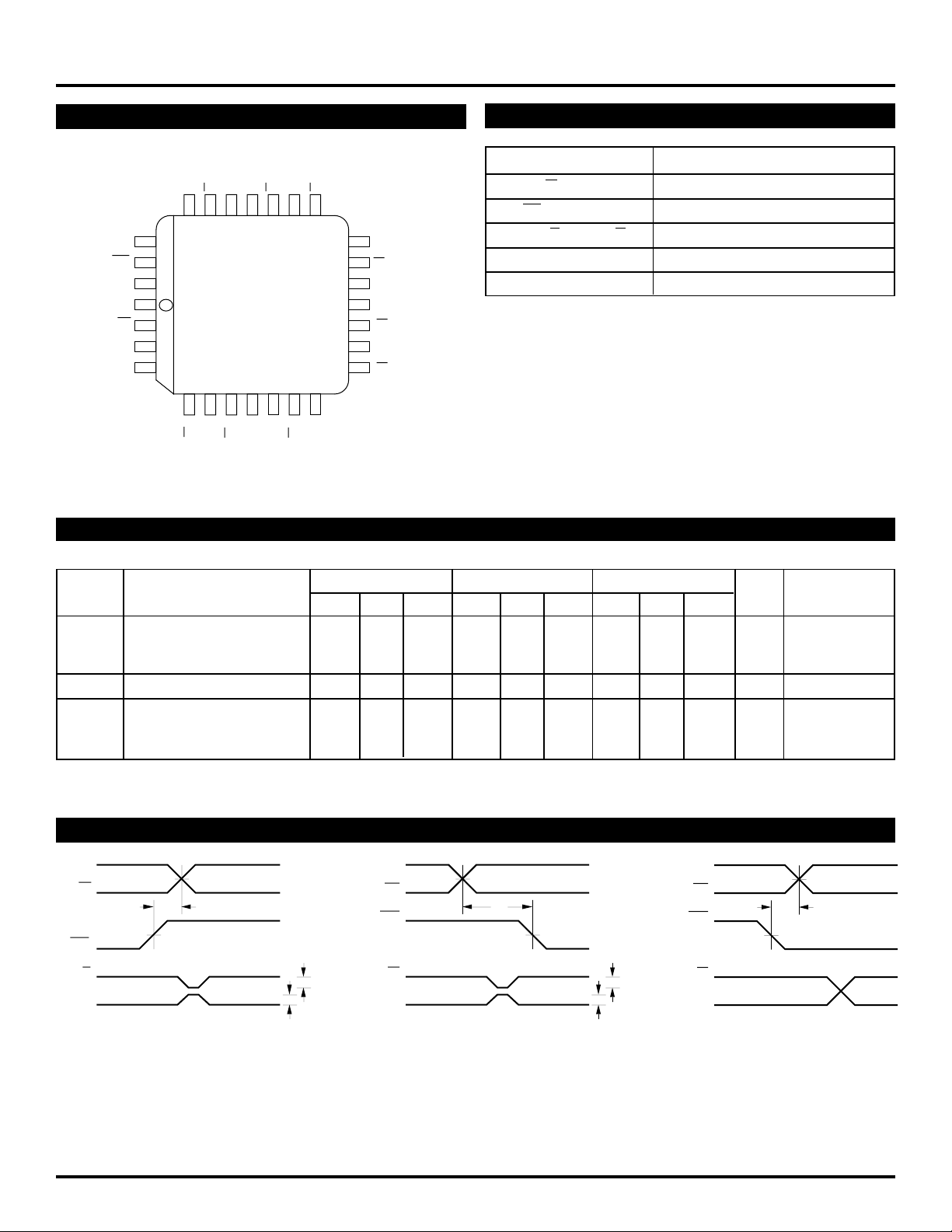
PIN CONFIGURATION
0
0
1
Q
Q
Q
24 23 22 21 20 19
25
V
EE
26
EN
V
V
NC
IN
CC
IN
BB
27
28
1
2
3
4
567891011
TOP VIEW
8
8
Q
Q
PLCC
J28-1
7
Q
CCO
V
CCO
V
2
2
1
Q
Q
Q
Q
18
17
16
15
14
13
12
6Q6
7
Q
Q
3
Q
3
Q
4
V
CCO
Q
4
Q
5
Q
5
PIN NAMES
Pin Function
IN, IN Differential Input Pair
EN Enable Input
Q0, Q0 — Q8, Q8 Differential Outputs
VBB VBB Output
CCO VCC to Output
V
DC ELECTRICAL CHARACTERISTICS
VEE = VEE (Min.) to VEE (Max.); VCC = VCCO = GND
TA = 0°CTA = +25°CTA = +85°C
Symbol Parameter Min. Typ. Max. Min. Typ. Max. Min. Typ. Max. Unit Condition
V
BB Output Reference V —
Voltage 10E –1.38 —–1.27 –1.35 —–1.25 –1.31 —–1.19
100E –1.38 —–1.26 –1.38 —–1.26 –1.38 —–1.26
IIH Input HIGH Current ——150 ——150 ——150 µA —
EE Power Supply mA —
I
Current 10E — 48 60 — 48 60 — 48 60
100E — 48 60 — 48 60 — 55 69
TIMING DIAGRAMS
IN
IN
t
s
50%
EN
75 mV
Q
Q
75 mV
Figure 1. Set-up Time
IN
IN
EN
Q
Q
Figure 2. Hold Time
t
h
50%
75 mV
75 mV
Figure 3. Release Time
2
 Loading...