

MICREL SY10E016, SY100E016 Datasheet
8-BIT SYNCHRONOUS
BINARY UP COUNTER
SY10E016
SY100E016
FEATURES
■ 700MHz min. count frequency
■ Extended 100E VEE range of –4.2V to –5.5V
■ 1000ps CLK to Q, TC
■ Internal, gated TC feedback
■ 8 bits wide
■ Fully synchronous counting and TC generation
■ Asynchronous Master Reset
■ Fully compatible with industry standard 10KH,
100K I/O levels
■ Internal 75KΩ input pulldown resistors
■ Fully compatible with Motorola MC10E/100E016
■ Available in 28-pin PLCC package
PIN CONFIGURATION
6
VCCO
TC
P5
18
Q7
17
Q6
16
VCC
Q5
15
14
VCCO
13
Q4
12
Q3
MR
CLK
TCLD
VEE
NC
P
P1
CE
PE
P7
P
25 24 23 22 21 20 19
26
27
28
1
2
0
3
4
567891011
PLCC
TOP VIEW
J28-1
DESCRIPTION
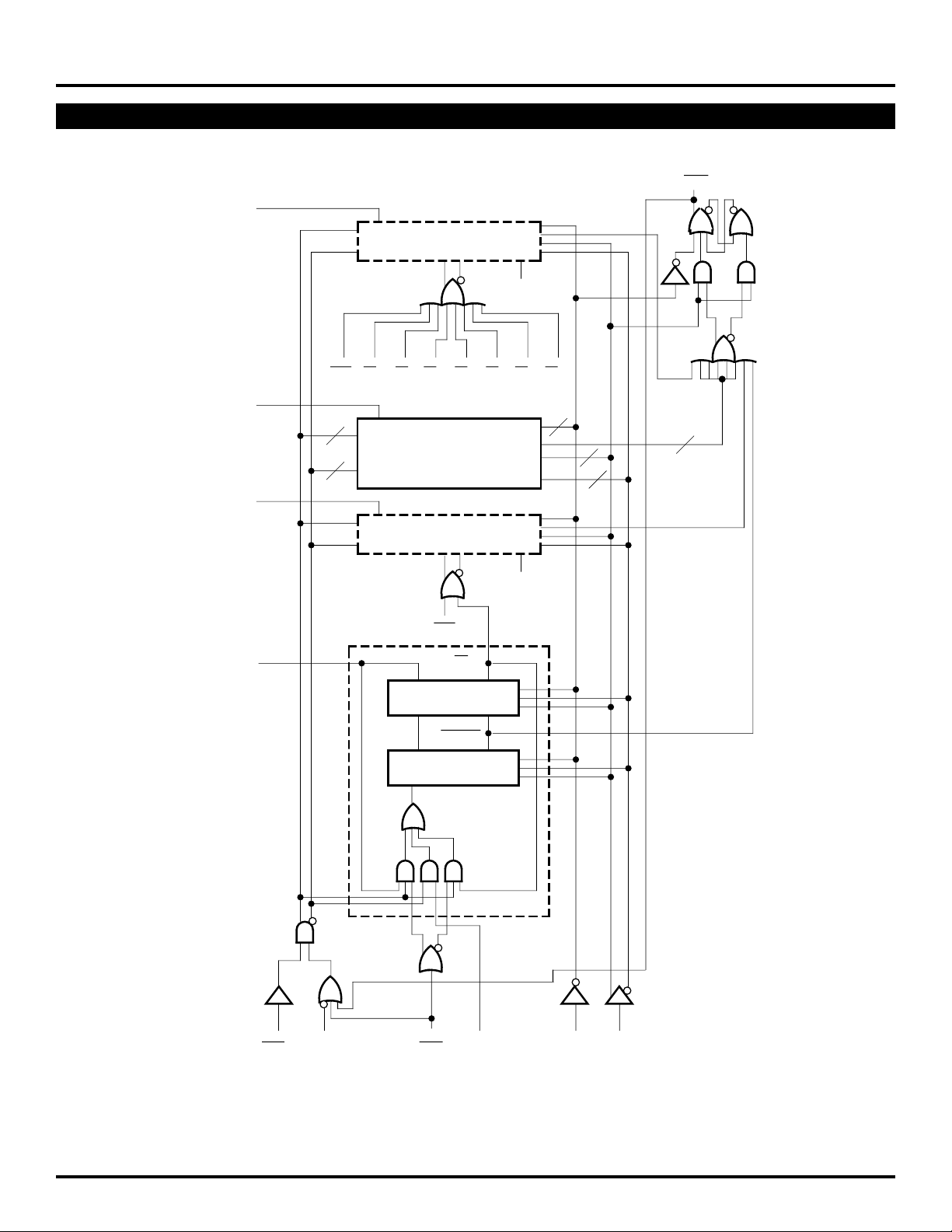
The SY10/100E016 are high-speed synchronous,
presettable and cascadable 8-bit binary counters designed
for use in new, high-performance ECL systems. Architecture
and operation are the same as the Motorola MC10H016 in
the MECL 10KH family, extended to 8 bits, as shown in the
logic diagram.
The counters feature internal feedback of TC, gated by
the TCLD (terminal count load) pin. When TCLD is LOW,
the TC feedback is disabled and counting proceeds
continuously, with TC going LOW to indicate an all-HlGH
state. When TCLD is HIGH, the TC feedback causes the
counter to automatically reload upon TC = LOW, thus
functioning as a programmable counter.
PIN NAMES
Pin Function
P0-P7 Parallel Data (Preset) Inputs
Q0-Q7 Data outputs
CE Count Enable Control Input
PE Parallel Load Enable Control Input
MR Master Reset
CLK Clock
TC Terminal Count Output
TCLD TC-Load Control Input
V
CCO VCC to Output
P4
P2
P3
VCCO
Q2
Q1
Q0
Rev.: D Amendment: /2
1
Issue Date: May, 1998
Micrel
BLOCK DIAGRAM
Q
SY10E016
SY100E016
TC
7
BIT 7
P
7
CE
Q
0Q1Q2Q3Q4Q5Q6
Q2 – Q
Q
Q
6
5
5
BIT 2 – BIT 6
5
5
5
1
5
BIT 1
P
1
CE
0
Q
0
SLAVE
Q0M
Q0M
MASTER
BIT 0
PE
TCLD MR CLK
CE
P
0
2
Micrel
SY10E016
SY100E016
TRUTH TABLE
(1)
CE PE TCLD MR CLK Function
X L X L Z Load Parallel (Pn to Qn)
L H L L Z Continuous Count
L H H L Z Count; Load Parallel on TC = LOW
H H X L Z Hold
X X X L ZZ Master respond, Slaves Hold
X X X H Z Reset (Q
NOTE:
1. Z = Clock Pulse (LOW-to-HIGH), ZZ = Clock Pulse (HIGH-to-LOW)
n : = LOW, TC : = HIGH)
DC ELECTRICAL CHARACTERISTICS
VEE = VEE (Min.) to VEE (Max.); VCC = VCCO = GND
TA = –40°CTA = 0°CTA = +25°CTA = +85°C
Symbol Parameter Min. Typ. Max. Min. Typ. Max. Min. Typ. Max. Min. Typ. Max. Unit
IIH Input HIGH Current — — 150 — — 150 — — 150 — — 150 µA
I
EE Power Supply Current mA
10E — 151 181 — 151 181 — 151 181 — 151 181
100E — 151 181 — 151 181 — 151 181 — 174 208
AC ELECTRICAL CHARACTERISTICS
VEE = VEE (Min.) to VEE (Max.); VCC = VCCO = GND
TA = –40°CTA = 0°CTA = 25°CTA = +85°C
Symbol Parameter Min. Typ. Max. Min. Typ. Max. Min. Typ. Max. Min. Typ. Max. Unit
fCOUNT Max. Count Frequency 700 900 — 700 900 — 700 900 — 700 900 — MHz
PLH Propagation Delay to Output ps
t
tPHL CLK to Q 600 725 1000 600 725 1000 600 725 1000 600 725 1000
MR to Q 600 775 1000 600 775 1000 600 775 1000 600 775 1000
CLK to TC (Qs loaded)
CLK to TC (Qs unloaded)
MR to TC 625 775 1000 625 775 1000 625 775 1000 625 775 1000
t
S Set-up Time ps
Pn 150 –30 — 150 –30 — 150 –30 — 150 –30 —
CE 600 400 — 600 400 — 600 400 — 600 400 —
PE 600 400 — 600 400 — 600 400 — 600 400 —
TCLD 500 300 — 500 300 — 500 300 — 500 300 —
H Hold Time ps
t
Pn 250 30 — 250 30 — 250 30 — 250 30 —
CE 0 –400 — 0 –400 — 0 –400 — 0 –400 —
PE 0 –400 — 0 –400 — 0 –400 — 0 –400 —
TCLD 100 –300 — 100 –300 — 100 –300 — 100 –300 —
tRR Reset Recovery Time 900 700 — 900 700 — 900 700 — 900 700 — ps
WP Minimum Pulse Width 400 — — 400 — — 400 — — 400 — — ps
t
CLK, MR
r Rise/Fall Times 300 510 800 300 510 800 300 510 800 300 510 800 ps
t
tf 20% to 80%
NOTE:
1. CLK to TC propagation delay is dependent on the loading of the Q outputs. With all of the Q outputs loaded, the noise generated in going from a IIII IIII
state to a 0000 0000 state causes the CLk to TC+ delay to increase.
(1)
550 775 1050 550 775 1050 550 775 1050 550 775 1050
(1)
550 700 900 550 700 900 550 700 900 550 700 900
3
 Loading...