

MICREL SY100S371 Datasheet
TRIPLE 4-INPUT
MULTIPLEXER
WITH ENABLE
FEATURES
■ Max. propagation delay of 1000ps
■ I
EE min. of –68mA
■ Industry standard 100K ECL levels
■ Extended supply voltage option:
VEE = –4.2V to –5.5V
■ Voltage and temperature compensation for improved
noise immunity
■ Internal 75KΩ input pull-down resistors
■ 40% faster than Fairchild
■ 40% lower power than Fairchild
■ Function and pinout compatible with Fairchild F100K
■ Available in 24-pin CERPACK and 28-pin PLCC
packages
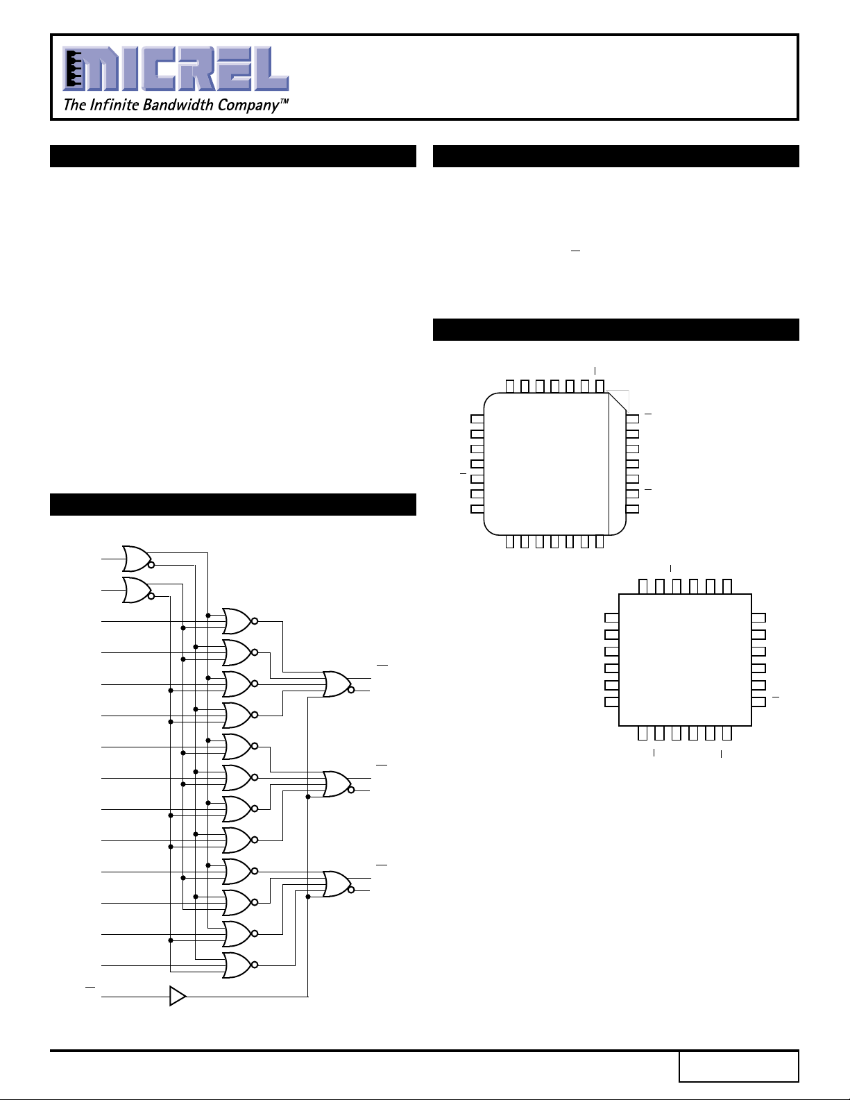
BLOCK DIAGRAM
SY100S371
DESCRIPTION
The SY100S371 is an ultra-fast triple 4-input multiplexer
with true and complementary outputs designed for use in
high-performance ECL systems. The multiplexer is
controlled by common select inputs S0 and S1. A logic
HIGH on the Enable (E) control input takes the outputs to
a logic LOW. The inputs on the device have 75KΩ pulldown resistors.
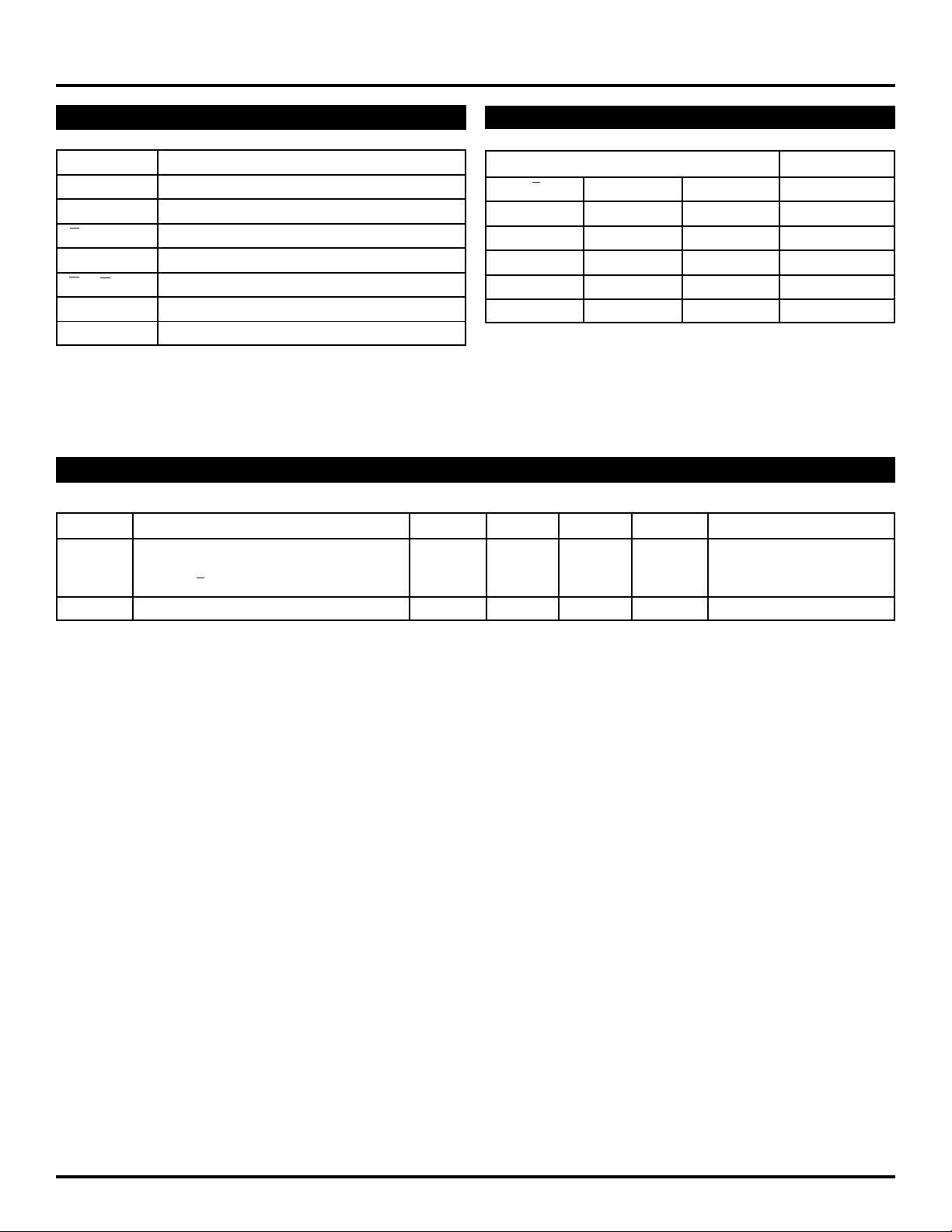
PIN CONFIGURATIONS
I3a
S0
S1
VEE
VEES
I0b
I1b
I2a
12
13
14
15
E
16
17
1911201021922823724
I1a
VEES
Top View
PLCC
J28-1
I0a
Za
Za
5
6
Zb
4
3
Zb
VCCA
2
1
VCC
VCC
28
27
Zc
2618
c
Z
25
S
0
S
1
I0c
I3b
I2b
VEES
I1c
I2c
I3c
I1bI0bE
EE
V
S1S
0
19
CCA
V
18
I
3a
17
I
2a
16
I
1a
15
I
0a
14
Z
a
13
Z
a
b
b
Z
Z
1
I
I
0a
I
1a
Z
I
2a
I
3a
I
0b
I
1b
I
2b
I
3b
I
0c
I
1c
I
2c
a
Z
a
Z
b
Z
b
Z
c
Z
c
2b
I
3b
2
3
I
0c
I
1c
I
2c
I
3c
Top View
Flatpack
4
F24-1
5
6
7248239221021112012
c
c
Z
Z
CC
V
I
3c
E
Rev.: G Amendment: /0
1
Issue Date: July, 1999
Micrel
SY100S371
PIN NAMES
Pin Function
I0X – I3X Data Inputs (x = a, b or c)
S0, S1 Select Inputs
E Enable Input (Active LOW)
Za – Zc Data Outputs
Za – Zc Complementary Data Outputs
VEES VEE Substrate
CCA VCCO for ECL Outputs
V
TRUTH TABLE
ES0 S1 Zn
LLLI0X
LHLI1X
LLHI2X
LHHI3X
HXXL
NOTE:
1. H = HIGH Voltage Level
L = LOW Voltage Level
X = Don't Care
(1)
Inputs Outputs
DC ELECTRICAL CHARACTERISTICS
VEE = –4.2V to –5.5V unless otherwise specified; VCC = VCCA = GND
Symbol Parameter Min. Typ. Max. Unit Condition
IH Input HIGH Current µAVIN = VIH (Max.)
I
I0X – I3X ——250
S0, S1, E — — 300
EE Power Supply Current –68 –48 –34 mA Inputs Open
I
2
 Loading...