


MICREL SY100S355 Datasheet
QUAD
R
MULTIPLEXER/LATCH
SY100S355
FEATURES
■ Max. propagation delay of 1100ps
■ Max. enable to output delay of 1400ps
■ IEE min. of –80mA
■ Industry standard 100K ECL levels
■ Extended supply voltage option:
VEE = –4.2V to –5.5V
■ Voltage and temperature compensation for improved
noise immunity
■ Internal 75KΩ input pull-down resistors
■ 50% faster than Fairchild
■ Function and pinout compatible with Fairchild F100K
■ Available in 24-pin CERPACK and 28-pin PLCC
packages
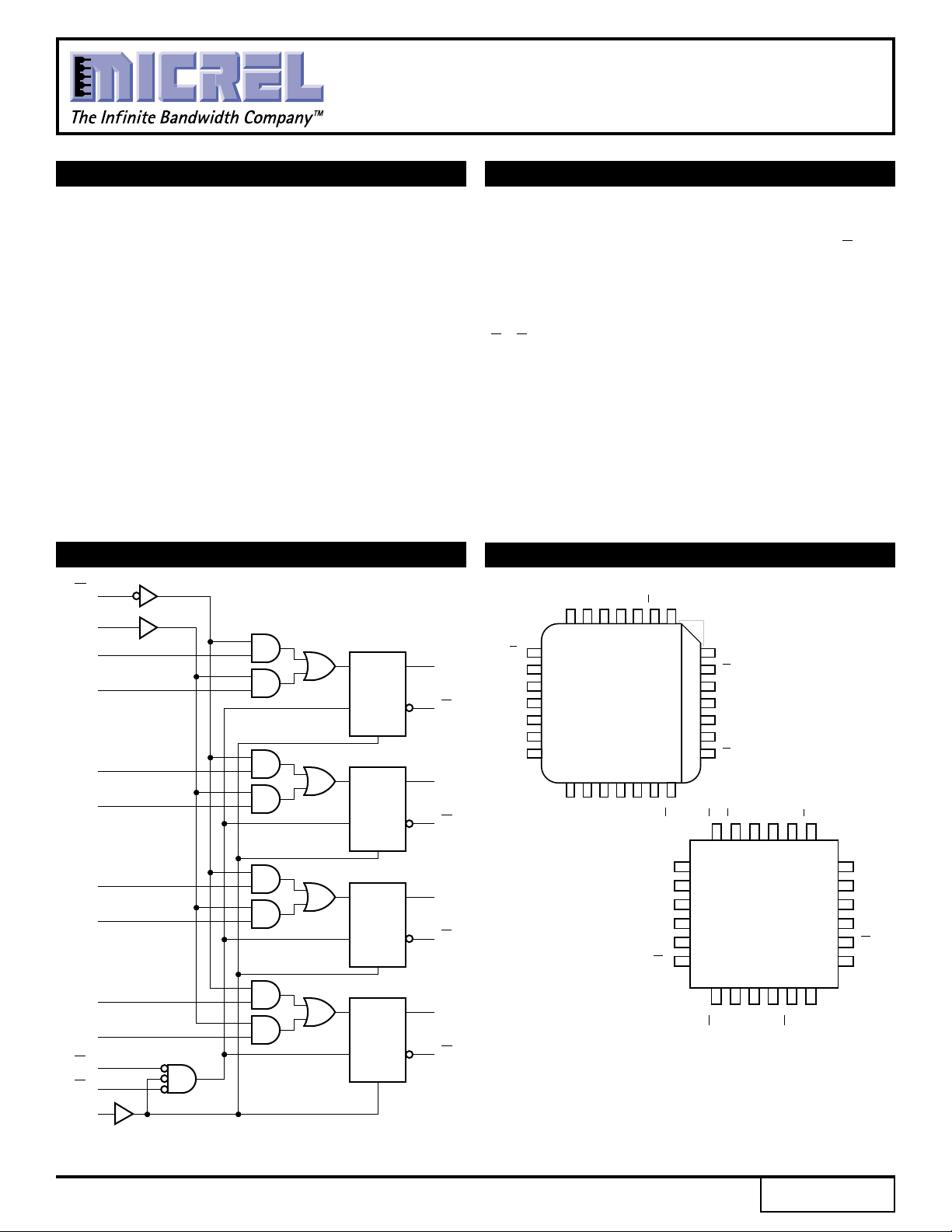
BLOCK DIAGRAM
S
0
S
1
D
D
D
D
D
D
D
D
E
E
MR
0a
1a
0b
1b
0c
1c
0d
1d
1
2
D
Q
E
CD
D
Q
E
CD
D
Q
E
CD
D
Q
E
CD
Q
a
Q
a
Q
b
Q
b
Q
c
Q
c
Q
d
Q
d
DESCRIPTION
The SY100S355 offers four transparent latches with
differential outputs and is designed for use in highperformance ECL systems. The Select inputs (S0, S1)
select one of the two sources of input data (D0 or D1) to the
latch. The Select inputs can also force the outputs to a logic
LOW when the latch is in the transparent mode. The
latches are in the transparent mode when both Enables
(E1, E2) are at a logic LOW state. In the transparent mode,
the Select inputs can pass an input logic HIGH from D0 or
D1 to the output.
If the Select inputs are tied together, then input data from
either D0 or D1 is always passed through. A rising edge on
either Enable input will latch the outputs with the most
recent data at the latch inputs being stored. The Master
Reset (MR) input overrides all other inputs and takes the Q
outputs to a logic LOW. The inputs on this device have
75KΩ pull-down resistors.
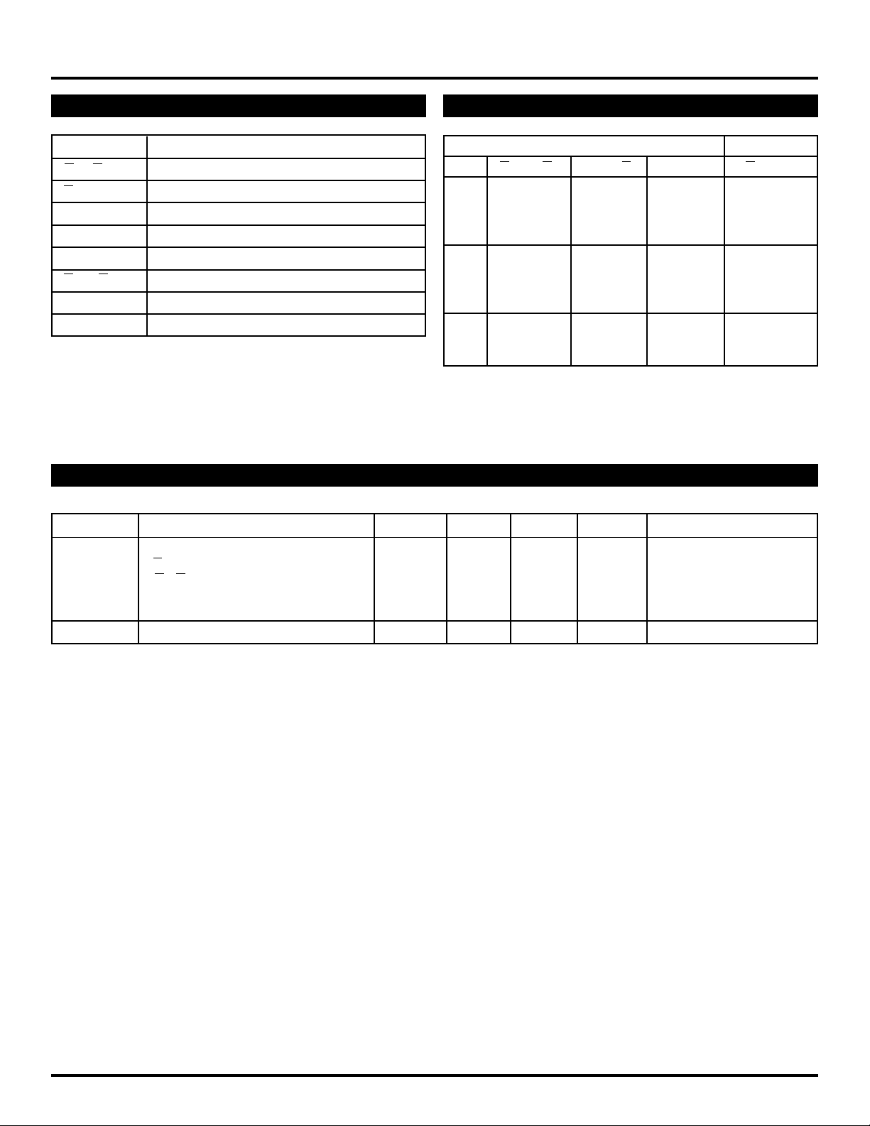
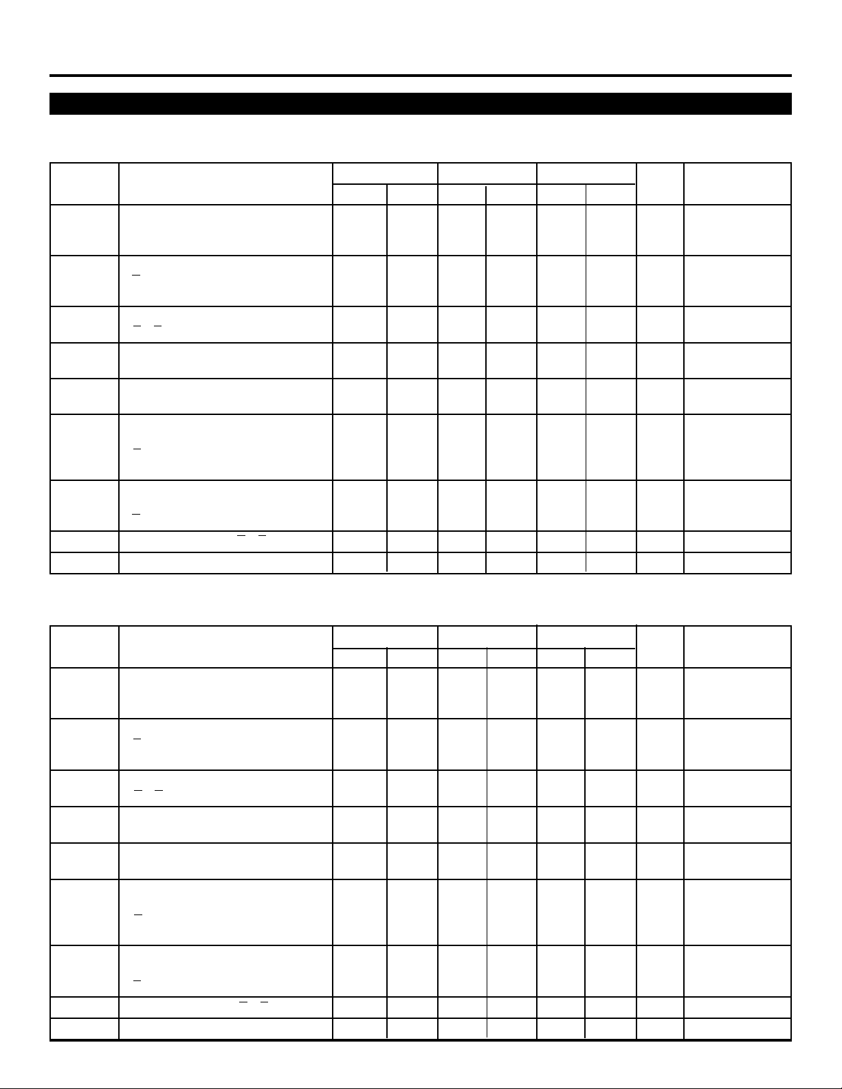
PIN CONFIGURATIONS
D1b
S0
S
VEE
VEES
MR
D0b
12
1
13
14
Top View
15
16
17
E1
E2
1911201021922823724
D1c
D0c
D1a
PLCC
J28-1
D0d
VEES
VEES
D0a
Qa
Qa
5
6
Qb
4
3
Qb
VCCA
2
1
VCC
VCC
28
27
Qc
2618
25
Qd
Qd
D1d
D
0c
D
1c
D
0d
D
1d
Q
d
Q
d
c
Q
E2E1M
1
2
3
Top View
Flatpack
4
5
6
F24-1
7248239221021112012
c
c
Q
CC
Q
V
EE
V
CCA
V
S1S
19
b
Q
0
b
Q
18
17
16
15
14
13
D
1b
D
0b
D
1a
D
0a
Q
a
Q
a
Rev.: G Amendment: /0
1
Issue Date: July, 1999
Micrel
SY100S355
PIN NAMES
TRUTH TABLE
Pin Function
E1 – E2 Enable Inputs (Active LOW)
S0, S1 Select Inputs
MR Master Reset
Dna – Dnd Data Inputs
Qa – Qd Data Outputs
Qa — Qd Complementary Data Outputs
VEES VEE Substrate
CCA VCCO for ECL Outputs
V
MR E1 E2 S1 S0 D1X D0X QX QX
H X X XXXX HL
L L L HHHX LH
LLLHHLX HL
LLLLLXH LH
LLLLLXL HL
LLLLHXX HL
LLLHLHX LH
LLLHLXH LH
LLLHLLL HL
L H X X X X X Latched
L X H X X X X Latched
NOTE:
1. H = High Voltage Level
L = Low Voltage Level
X = Don't Care
DC ELECTRICAL CHARACTERISTICS
VEE = –4.2V to –5.5V unless otherwise specified; VCC = VCCA = GND
(1)
Inputs Outputs
Symbol Parameter Min. Typ. Max. Unit Condition
IH Input HIGH Current µAVIN = VIH (Max.)
I
S0, S1 ——220
E1, E2 ——350
Dna, Dnd ——340
MR — — 430
EE Power Supply Current –80 –57 –40 mA Inputs Open
I
2
Micrel
SY100S355
AC ELECTRICAL CHARACTERISTICS
CERPACK
VEE = –4.2V to –5.5V unless otherwise specified; VCC = VCCA = GND
T
A = 0°CTA = +25°CTA = +85°C
Symbol Parameter Min. Max. Min. Max. Min. Max. Unit Condition
t
PLH Propagation Delay 300 1200 300 1200 300 1200 ps
PHL Dna – Dnd to Output
t
(Transparent Mode)
t
PLH Propagation Delay 300 1500 300 1500 300 1500 ps
tPHL S0, S1 to Output
(Transparent Mode)
PLH Propagation Delay 300 1500 300 1500 300 1500 ps
t
tPHL E1, E2 to Output
PLH Propagation Delay 300 1200 300 1200 300 1200 ps
t
tPHL MR to Output
tTLH Transition Time 300 900 300 900 300 900 ps
tTHL 20% to 80%, 80% to 20%
S Set-up Time ps
t
Dna – Dnd 700 — 700 — 700 —
S0, S1 1200 — 1200 — 1200 —
MR (Release Time) 1000 — 1000 — 1000 —
H Hold Time ps
t
Dna – Dnd 400 — 400 — 400 —
S0, S1 400 — 400 — 400 —
tPW (L) Pulse Width LOW, E1, E2 1000 — 1000 — 1000 — ps
PW (H) Pulse Width HIGH, MR 1000 — 1000 — 1000 — ps
t
PLCC
VEE = –4.2V to –5.5V unless otherwise specified; VCC = VCCA = GND
TA = 0°CTA = +25°CTA = +85°C
Symbol Parameter Min. Max. Min. Max. Min. Max. Unit Condition
PLH Propagation Delay 300 1100 300 1100 300 1100 ps
t
tPHL Dna – Dnd to Output
(Transparent Mode)
PLH Propagation Delay 300 1400 300 1400 300 1400 ps
t
tPHL S0, S1 to Output
(Transparent Mode)
PLH Propagation Delay 300 1400 300 1400 300 1400 ps
t
tPHL E1, E2 to Output
PLH Propagation Delay 300 1100 300 1100 300 1100 ps
t
tPHL MR to Output
t
TLH Transition Time 300 900 300 900 300 900 ps
tTHL 20% to 80%, 80% to 20%
S Set-up Time ps
t
Dna – Dnd 700 — 700 — 700 —
S0, S1 1200 — 1200 — 1200 —
MR (Release Time) 1000 — 1000 — 1000 —
H Hold Time ps
t
Dna – Dnd 300 — 300 — 300 —
S0, S1 300 — 300 — 300 —
tPW (L) Pulse Width LOW, E1, E2 1000 — 1000 — 1000 — ps
PW (H) Pulse Width HIGH, MR 1000 — 1000 — 1000 — ps
t
3