

MICREL SY100S350 Datasheet
HEX D-LATCH
R
SY100S350
FEATURES
■ Max. transparent propagation delay of 900ps
■ Min. Master Reset and Enable pulse widths of 100ps
■ IEE min. of –98mA
■ Industry standard 100K ECL levels
■ Extended supply voltage option:
VEE = –4.2V to –5.5V
■ Voltage and temperature compensation for improved
noise immunity
■ Internal 75KΩ input pull-down resistors
■ More than 40% faster than Fairchild
■ Approximately 30% lower power than Fairchild
■ Function and pinout compatible with Fairchild F100K
■ Available in 24-pin CERPACK and 28-pin PLCC
packages
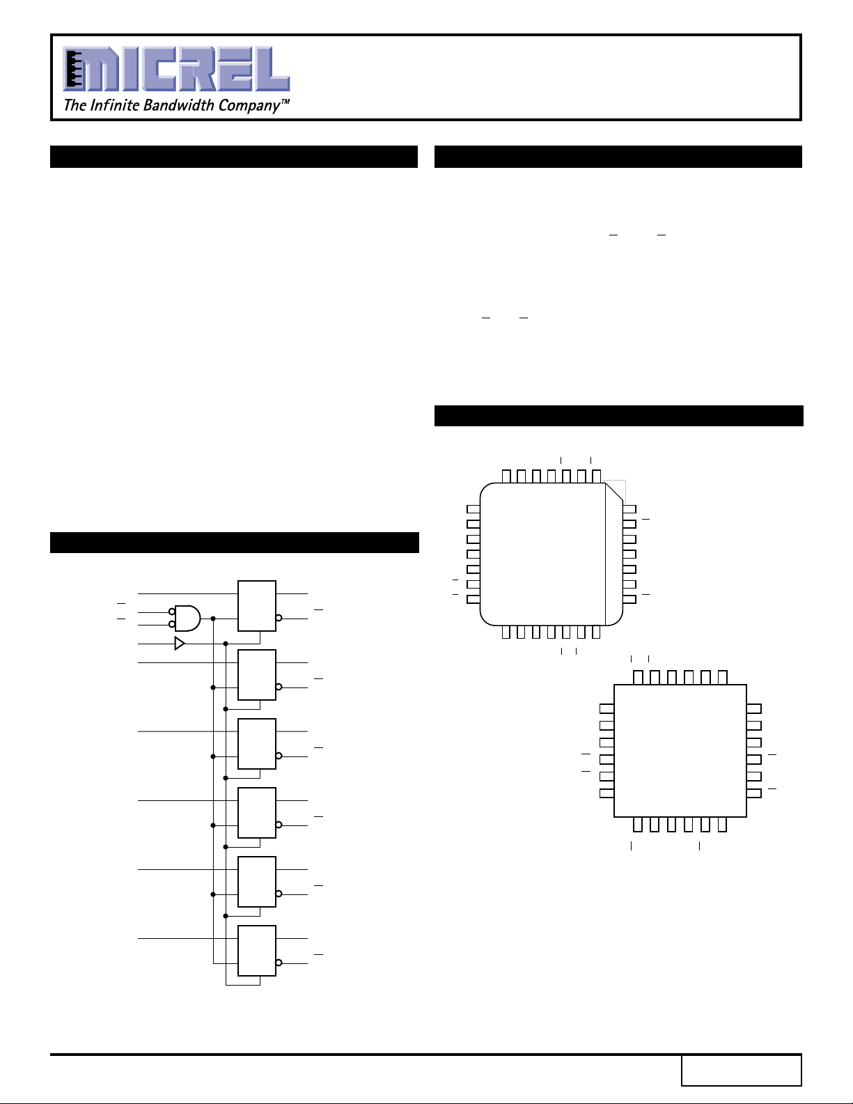
BLOCK DIAGRAM
D
E
E
MR
D
5
b
a
4
D
E Q
R
D
Q
5
5
Q
4
DESCRIPTION
The SY100S350 offers six high-speed D-Latches with
both true and complement outputs, and is performance
compatible for use with high-performance ECL systems.
When both enable signals (E
a and Eb) are at a logic LOW,
the latches are transparent and the input signals( D0–D5)
appear at the outputs (Q0–Q5) after a propagation delay. If
either or both of the enable signals are at a logic HIGH, then
the latches store the last valid data present on its inputs
before Ea or Eb went to a logic HIGH. The Master Reset
(MR) overrides all other input signals and takes the outputs
to a logic LOW state. All inputs have 75KΩ pull-down
resistors.
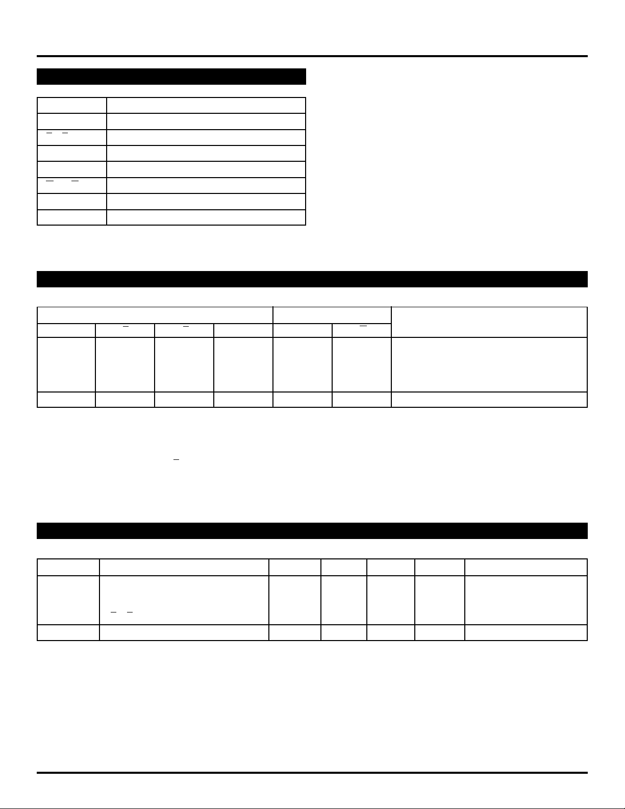
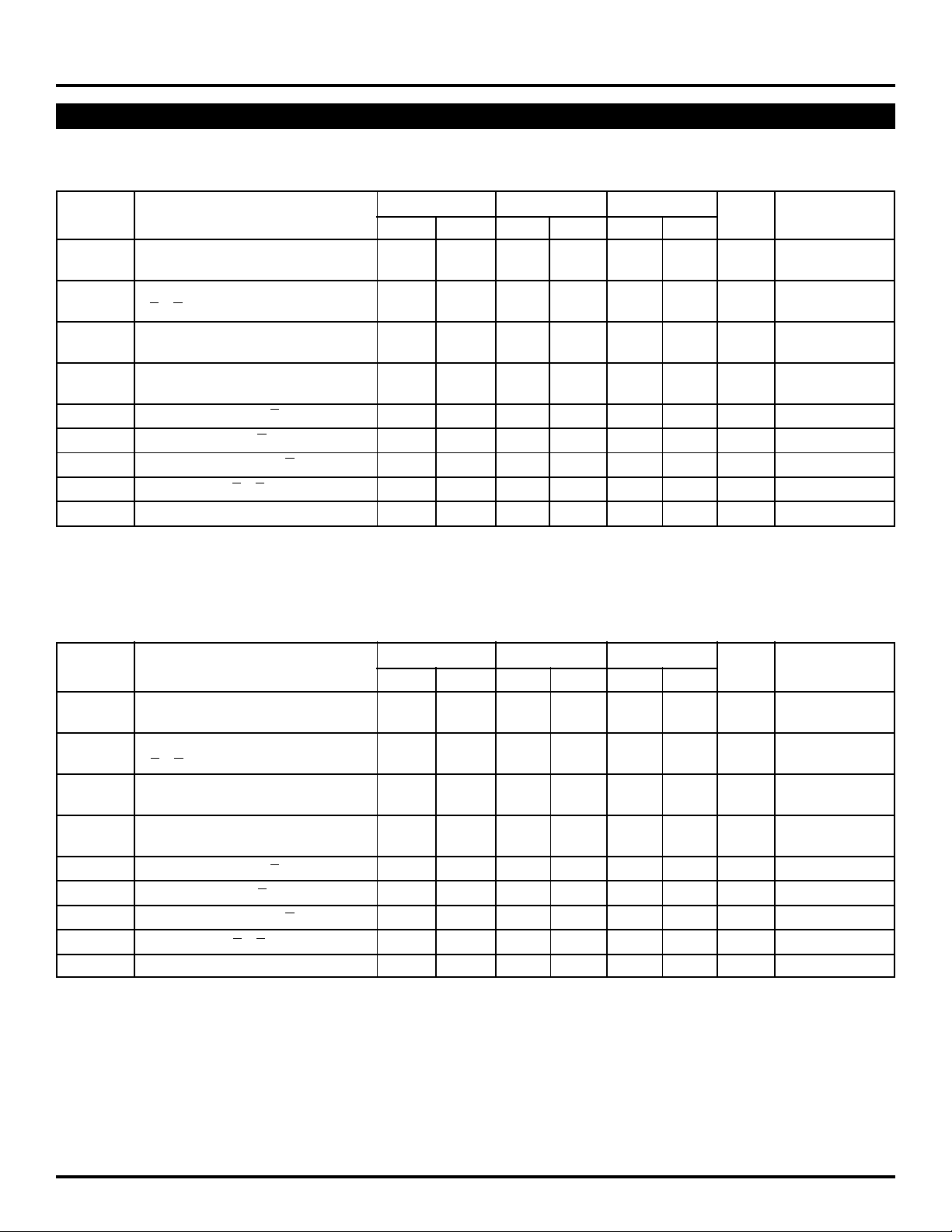
PIN CONFIGURATIONS
D1
D0
Q0
Q0Q1Q1
VEES
6
5
D2
D
VEE
VEES
MR
Ea
12
13
3
14
Top View
15
16
17
PLCC
J28-1
1911201021922823724
D5
Q5
D4
Q5
VEES
25
Q4
Q2
4
3
Q2
2
VCCA
1
VCC
28
VCC
27
Q3
2618
Q
3Eb
Q4
EbEaM
VEED3D
2
E Q
R
D
3
D
2
D
1
0
D
D
E Q
R
D
E Q
R
D
E Q
R
D
E Q
R
4
1
D
4
D
5
Q
3
3
Q
2
2
Q
1
1
Q
0
0
2
3
Q
5
Q
5
Q
4
Q
4
Top View
Flatpack
4
F24-1
5
6
7248239221021112012
3
3
Q
Q
1
19
18
17
16
15
14
13
2
CC
V
2
Q
Q
CCA
V
Rev.: G Amendment: /0
Issue Date: July, 1999
D
1
D
0
Q
0
Q
0
Q
1
Q
1
Micrel
PIN NAMES
Pin Function
D0 — D5 Data Inputs
Ea, Eb Common Enable Inputs (Active LOW)
MR Asynchronous Master Reset Input
Q0 — Q5 Data Outputs
Q0 — Q5 Complementary Data Outputs
VEES VEE Substrate
CCA VCCO for ECL Outputs
V
SY100S350
TRUTH TABLE
(1)
Each Latch
Inputs Outputs
Dn Ea Eb MR Qn Qn Operating Mode
H L L L H L Latch
LLLLLH
X X H L Latched
X H X L Latched
(2)
Latched
(2)
Latched
(2)
(2)
X X X H L H Asynchronous
NOTES:
1. H = HIGH State
L = LOW State
X = Don't Care
2. Retains data that is present before E positive transition.
DC ELECTRICAL CHARACTERISTICS
VEE = –4.2V to –5.5V unless otherwise specified; VCC = VCCA = GND
Symbol Parameter Min. Typ. Max. Unit Condition
I
IH Input HIGH Current µAVIN = VIH (Max.)
MR ——250
Dn ——250
Ea, Eb ——250
EE Power Supply Current –98 –78 –49 mA Inputs Open
I
2
Micrel
SY100S350
AC ELECTRICAL CHARACTERISTICS
CERPACK
VEE = –4.2V to –5.5V unless otherwise specified; VCC = VCCA = GND
TA = 0°CTA = +25°CTA = +85°C
Symbol Parameter Min. Max. Min. Max. Min. Max. Unit Condition
t
PLH Propagation Delay 300 1000 300 1000 300 1000 ps
tPHL Dn to Output
PLH Propagation Delay 300 1100 300 1100 300 1100 ps
t
tPHL Ea, Eb to Output
PLH Propagation Delay 300 1250 300 1250 300 1250 ps
t
tPHL MR to Output
TLH Transition Time 300 900 300 900 300 900 ps
t
tTHL 20% to 80%, 80% to 20%
tS Set-up Time, Dn to En 500 — 500 — 500 — ps
tH Hold Time, Dn to En 500 — 500 — 500 — ps
tr Release Time, MR to En 1000 — 1000 — 1000 — ps
tPW (L) Pulse Width, Ea, Eb 1000 — 1000 — 1000 — ps
PW (H) Pulse Width, MR 1000 — 1000 — 1000 — ps
t
PLCC
VEE = –4.2V to –5.5V unless otherwise specified; VCC = VCCA = GND
A = 0°CTA = +25°CTA = +85°C
T
Symbol Parameter Min. Max. Min. Max. Min. Max. Unit Condition
PLH Propagation Delay 300 900 300 900 300 900 ps
t
tPHL Dn to Output
t
PLH Propagation Delay 300 1000 300 1000 300 1000 ps
tPHL Ea, Eb to Output
PLH Propagation Delay 300 1200 300 1200 300 1200 ps
t
tPHL MR to Output
TLH Transition Time 300 900 300 900 300 900 ps
t
tTHL 20% to 80%, 80% to 20%
tS Set-up Time, Dn to En 500 — 500 — 500 — ps
tH Hold Time, Dn to En 500 — 500 — 500 — ps
tr Release Time, MR to En 1000 — 1000 — 1000 — ps
tPW (L) Pulse Width, Ea, Eb 1000 — 1000 — 1000 — ps
PW (H) Pulse Width, MR 1000 — 1000 — 1000 — ps
t
3
 Loading...