

MICREL SY100S341 Datasheet
8-BIT SHIFT
REGISTER
SY100S341
FEATURES
■ Max. shift frequency of 600MHz
■ Max. Clock to Q delay of 1200ps
■ IEE min. of –150mA
■ Industry standard 100K ECL levels
■ Extended supply voltage option:
VEE = –4.2V to –5.5V
■ Voltage and temperature compensation for improved
noise immunity
■ Internal 75KΩ input pull-down resistors
■ 70% faster than Fairchild 300K at lower power
■ Function and pinout compatible with Fairchild F100K
■ Available in 24-pin CERPACK and 28-pin PLCC
packages
PIN NAMES
Label Function
CP Clock Pulse Input
S0 — S1 Select Inputs
D0 — D7 Serial Inputs
P0 — P7 Parallel Inputs
Q0 — Q7 Data Outputs
VEES VEE Substrate
V
CCA VCCO for ECL Outputs
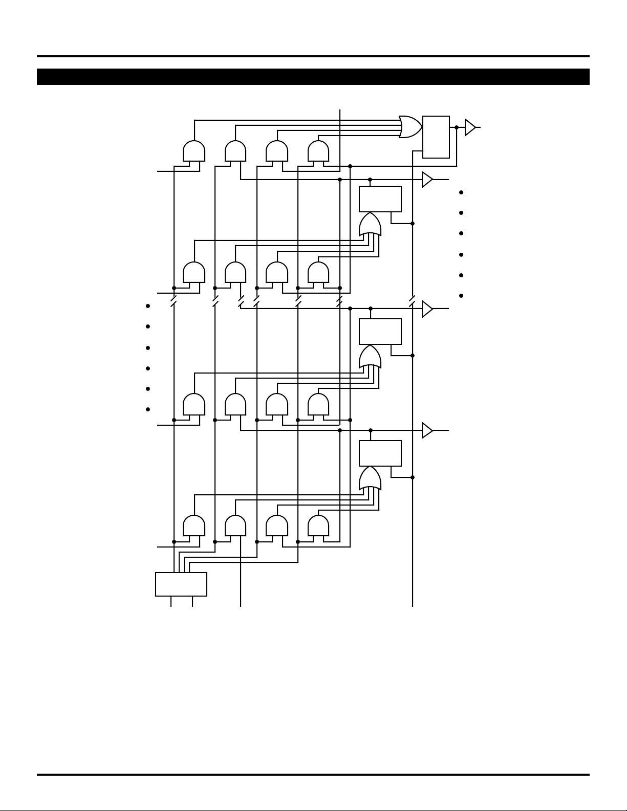
DESCRIPTION
The SY100S341 offer eight D-type, edge-triggered flipflops with both individual inputs for parallel operation as
well as serial inputs for bidirectional shifting, and are
designed for use in high-performance ECL systems. Data
is clocked into the flip-flops on the rising edge of the clock.
The mode of operation is selected by two Select inputs
(S0, S1) which determine if the device performs a shift, hold
or parallel entry function, as described in the Truth Table.
The inputs on these devices have 75KΩ pull-down resistors.
PIN CONFIGURATIONS
P4
CP
VEE
VEES
S0
S
12
13
14
15
16
17
1
18
P5P6P7
1911201021922823724
P1D0P2
VEES
Top View
PLCC
J28-1
P0
VEES
D7
Q7
Q6
5
6
4
Q5
3
Q4
2
VCCA
1
VCC
28
VCC
27
Q3
26
25
Q1
Q0
2P3
Q
P3S1S
0
EE
V
CP
4
P
19
1
P
2
P
1
2
3
P
0
D
0
Q
0
Q
1
Top View
Flatpack
4
F24-1
5
6
18
17
16
15
14
13
P
5
P
6
P
7
D
7
Q
7
Q
8
7248239221021112012
3
2
Q
Q
1
4
CC
V
5
Q
Q
CCA
V
Rev.: G Amendment: /0
Issue Date: July, 1999
Micrel
BLOCK DIAGRAM
D
SY100S341
7
P
P
DCQ
7
Q
DC
6
Q
Q
Q
DC
Q
7
6
1
P
1
PARALLEL
LOAD
P
0
SHIFT
LEFT
DECODE
S0S
1
SHIFT
RIGHT
D
0
HOLD
Q
DC
CP
Q
0
2
Micrel
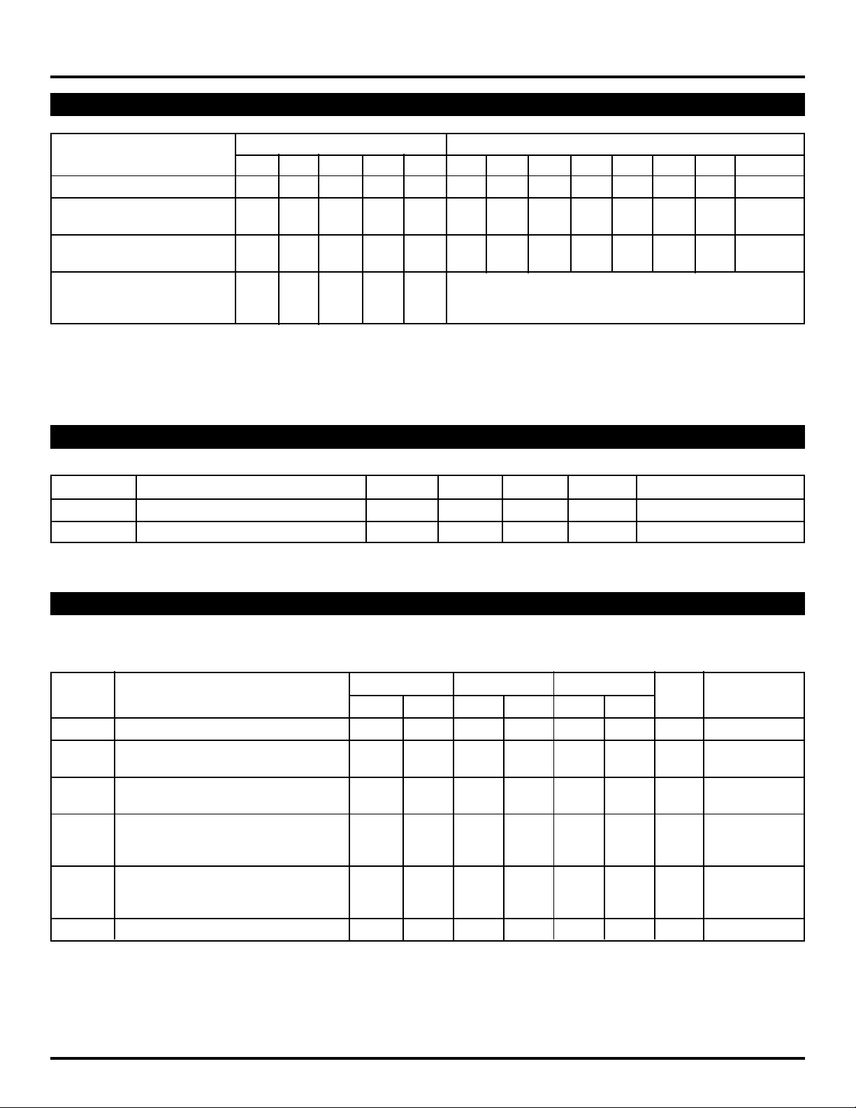
TRUTH TABLE
Inputs Outputs
Function D7 D0 S1 S0 CP Q7 Q6 Q5 Q4 Q3 Q2 Q1 Q0
Load Register X X L L u P7 P6 P5 P4 P3 P2 P1 P0
Shift Left X L L H u Q6 Q5 Q4 Q3 Q2 Q1 Q0 L
Shift Left X H L H u Q6 Q5 Q4 Q3 Q2 Q1 Q0 H
Shift Right L X H L u L Q
7 Q6 Q5 Q4 Q3 Q2 Q1
Shift Right H X H L u H Q7 Q6 Q5 Q4 Q3 Q2 Q1
Hold X X H H X No Change
Hold XXXXH
Hold XXXXL
NOTE:
1. H = HIGH Voltage Level
L = LOW Voltage Level
X = Don't Care
u = LOW-to-HIGH Transition
DC ELECTRICAL CHARACTERISTICS
VEE = –4.2V to –5.5V unless otherwise specified; VCC = VCCA = GND
SY100S341
Symbol Parameter Min. Typ. Max. Unit Condition
IIH Input HIGH Current, All Inputs ——200 µAVIN = VIH (Max.)
EE Power Supply Current –150 –102 –71 mA Inputs Open
I
AC ELECTRICAL CHARACTERISTICS
CERPACK
VEE = –4.2V to –5.5V unless otherwise specified; VCC = VCCA = GND
TA = 0°CTA = +25°CTA = +85°C
Symbol Parameter Min. Max. Min. Max. Min. Max. Unit Condition
fshift Shift Frequency 600 — 600 — 600 — MHz
PLH Propagation Delay 450 1200 450 1200 450 1200 ps
t
tPHL CP to Output
TLH Transition Time 300 900 300 900 300 900 ps
t
tTHL 20% to 80%, 80% to 20%
S Set-up Time ps
t
Dn, Pn 300 — 300 — 300 —
Sn 600 — 600 — 600 —
H Hold Time ps
t
Dn, Pn 300 — 300 — 300 —
Sn 0 — 0 — 0 —
t
pw (H) Pulse Width HIGH, CP — 600 — 600 — 600 ps
3
 Loading...