

MICREL SY100S324 Datasheet
LOW POWER HEX
L
TTL-to-ECL
TRANSLATOR
SY100S324
FEATURES
■ Max. propagation delay of 1.4ns
■ IEE min. of –70mA
■ Industry standard 100K ECL levels
■ Extended supply voltage option:
VEE = –4.2V to –5.5V
■ Differential outputs
■ Voltage and temperature compensation for improved
noise immunity
■ Internal 75KΩ input pull-down resistors
■ Twice as fast as Fairchild’s 324
■ Function and pinout compatible with Fairchild F100K
■ Available in 24-pin CERPACK and 28-pin PLCC
packages
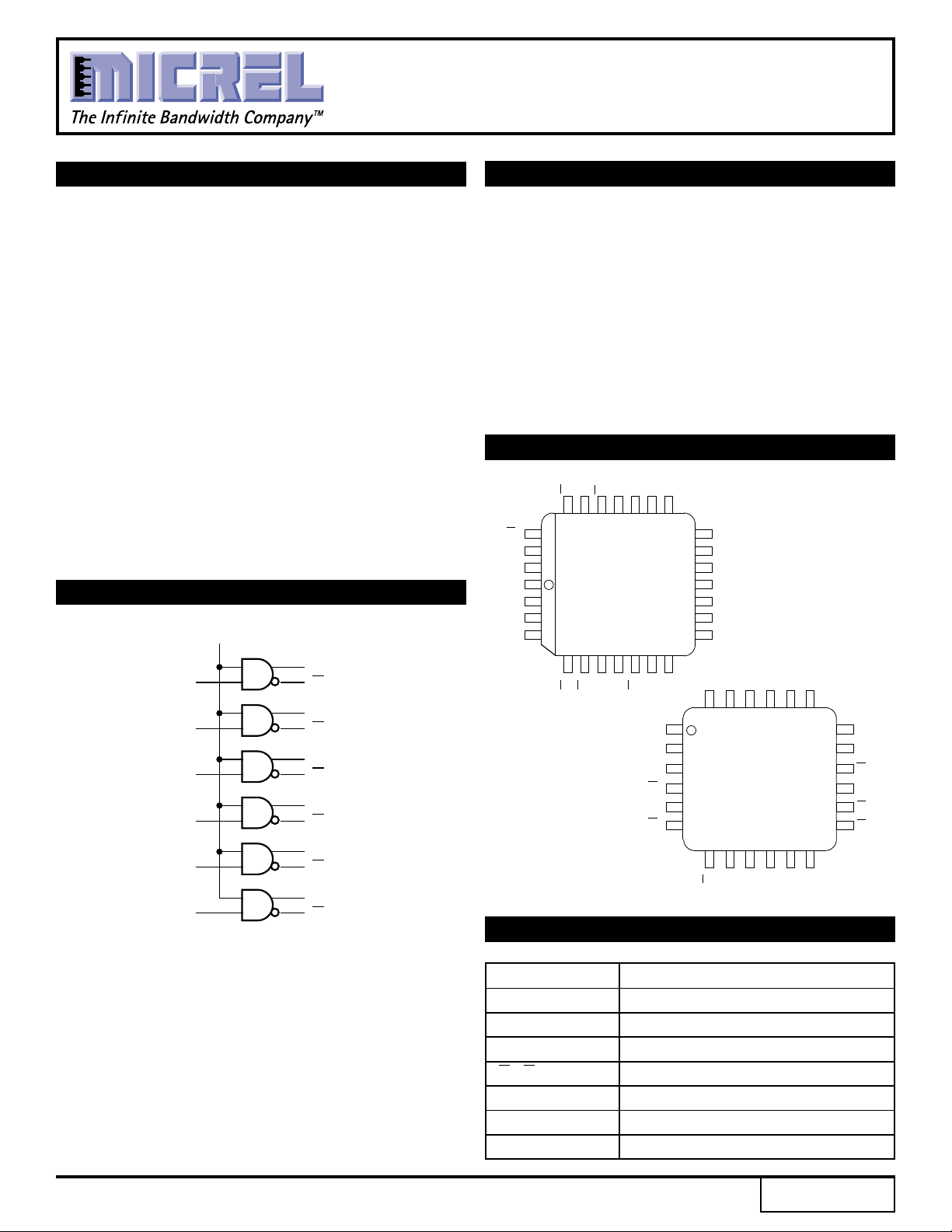
BLOCK DIAGRAM
E
Q
D
0
D
1
D
2
D
3
D
4
D
5
0
Q
0
Q
1
Q
1
Q
2
Q
2
Q
3
Q
3
Q
4
Q
4
Q
5
Q
5
DESCRIPTION
The SY100S324 is a hex translator designed to convert
TTL logic levels to 100K ECL levels. The inputs are TTL
compatible with differential outputs that can either be
used as an inverting/non-inverting translator or as
differential line drivers. A common Enable (E), when LOW,
holds all inverting outputs HIGH and holds all noninverting outputs LOW.
When used in the differential mode, due to its high
common mode rejection, it overcomes voltage gradients
between the TTL and ECL ground systems. The VEE and
VTTL power may be applied in either order.
PIN CONFIGURATIONS
1
0
EES
V
Q
Q1Q
25
24 23 22 21 20 19
26
Q
2
27
Q
2
28
V
CC
1
V
CC
CCA
CCA
Q
2
3
4
3
V
V
Top View
PLCC
J28-1
567891011
4
4
Q
Q3Q
EES
V
Q0D
5
Q
D
D
Q
Q
Q
Q
1
2
D
18
D
0
17
V
TTL
16
E
15
V
EES
14
V
EE
13
D
3
12
D
4
0
5
5
D
Q
1
2
0
0
1
1
TT
D
E
V
24 23 22 21 20 19
1
2
3
4
5
6
Top View
Flatpack
F24-1
7891011
2
2
CC
Q
Q
V
EE
V
CCA
V
3
D
CCA
V
4
D
18
D
5
17
Q
5
16
Q
5
15
Q
4
14
Q
4
13
Q
3
12
3
Q
PIN NAMES
Pin Function
D0–D5 Data Inputs
E Enable Inputs
Q0–Q5 Data Outputs
Q0–Q5 Complementary Data Outputs
VEES VEE Substrate
VTTL TTL VCC Power Supply
CCA VCCO for ECL Outputs
V
Rev.: F Amendment: /0
1
Issue Date: July, 1999
Micrel
SY100S324
DC ELECTRICAL CHARACTERISTICS
VEE = –4.2V to –5.5V unless otherwise specified, VCC = VCCA = GND, VTTL = +4.5V to +5.5V
Symbol Parameter Min. Sim. Max. Unit Condition
OH Output HIGH Voltage –1025 –986 –880 mV VIN = VIH (Max.) Loading with 50Ω
V
VOL Output LOW Voltage –1810 –1674 –1620 mV VIN = VIL (Min.)
OHC Output HIGH Voltage –1035 ——mV VIN = VIH (Min.) Loading with 50Ω to –2V
V
VOLC Output LOW Voltage ——–1610 mV VIN = VIL (Max.)
VIH Input HIGH Voltage 2.0 — 5.0 V Guaranteed HIGH Signal for All Inputs
VIL Input LOW Voltage 0 — 0.8 V Guaranteed LOW Signal for All Inputs
VCD Input Clamp Diode Voltage ——–1.5 V IIN = –10mA
IH Input HIGH Current
I
Data ——20 µAVIN = +2.4V
Enable ——120 All Other Inputs VIN = GND
IH Input HIGH Current ——1.0 mA VIN = +5.5V, VTTL = Max.,
I
Breakdown Test, All Inputs All Other Inputs VIN = GND
IL Input LOW Current
I
Data –1.2 ——mA VIN = +0.4V
Enable –6.7 —— All Other Inputs VIN = VIH
IEE VEE Power Supply Current –70 –45 –28 mA All Inputs VIN = +4.0V
I
TTL VTTL Power Supply Current — 25 35 mA All Inputs VIN = GND
AC ELECTRICAL CHARACTERISTICS
PLCC /FLATPACK
VEE = –4.2V to –5.5V unless otherwise specified, VCC = VCCA = GND, VTTL = +4.5V to +5.5V
Symbol Parameter Min. Typ. Max. Unit Condition
PLH Propagation Delay 400 850 1400 ps See Switching Wave Form Figures
t
tPHL Data and Enable to Output
TLH Transition Time 350 — 1700 ps
t
tTHL 20% to 80%, 80% to 20%
2
 Loading...