

MICREL SY100S313 Datasheet
QUAD DRIVER
4
3
2
8
7
6
SY100S313
FEATURES
■ Max. propagation delay of 800ps
■ Enable to Output max. of 950ps
■ IEE min. of –60mA
■ Extended supply voltage option:
VEE = –4.2V to –5.5V
■ Voltage and temperature compensation for
improved noise immunity
■ Internal 75KΩ input pull-down resistors
■ 50% faster than Fairchild 300K
■ Function and pinout compatible with Fairchild F100K
■ Available in 24-pin CERPACK and 28-pin PLCC
packages
BLOCK DIAGRAM
O
1a
D
a
D
b
D
c
D
d
E
O
2a
O
1a
O
2a
O
1b
O
2b
O
1b
O
2b
O
1c
O
2c
O
1c
O
2c
O
1d
O
2d
O
1d
O
2d
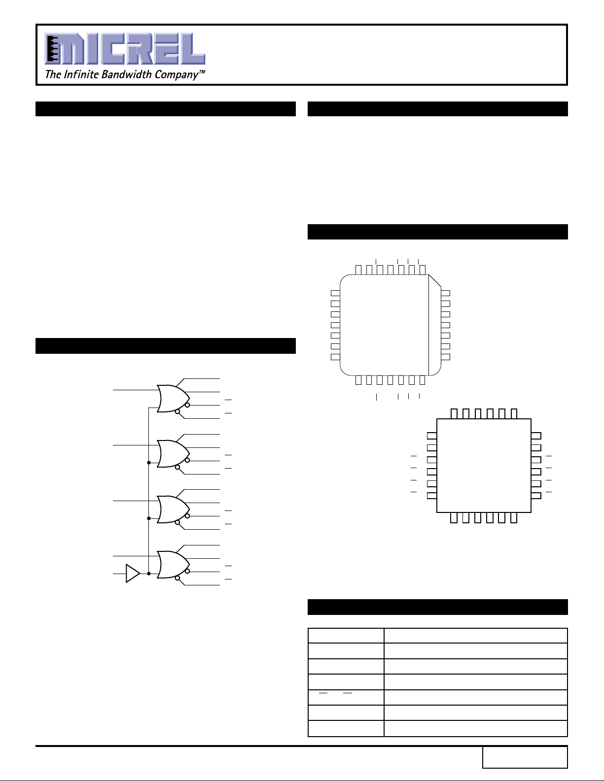
DESCRIPTION
The SY100S313 offers four drivers with two OR and two
NOR outputs, designed for use in high-performance ECL
systems. The four drivers are controlled by a common
Enable signal which is buffered to minimize input loading.
If the D inputs are not used, the Enable signal can be used
to drive sixteen 50Ω lines. All inputs have 75KΩ pulldown
resistors and all outputs are buffered.
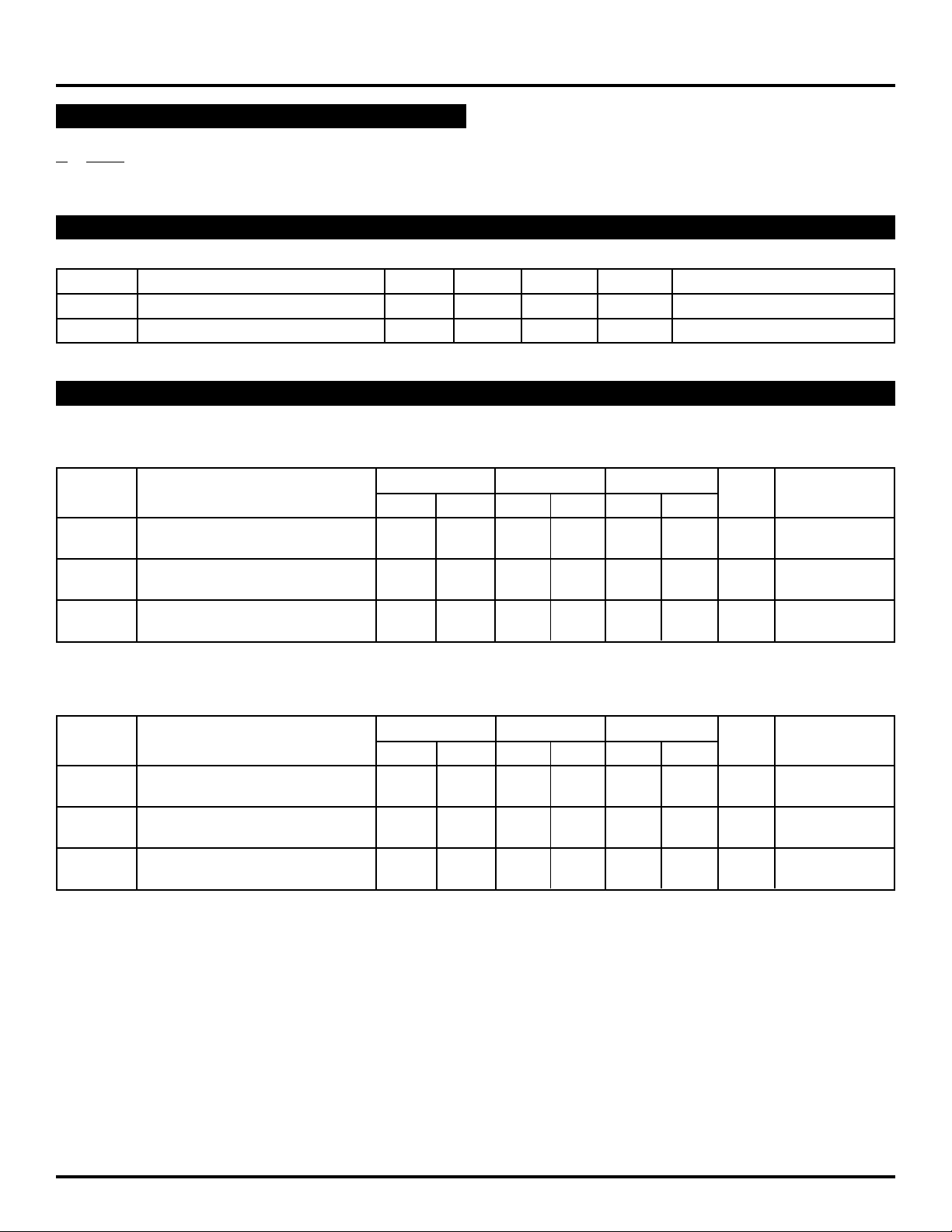
PIN CONFIGURATIONS
1a
O
O2aOaV
D
a
12
D
b
13
V
EE
14
Top View
V
EES
15
E
16
D
c
17
D
d
18
1911201021922823724
2d
1d
o
O
PLCC
J28-1
1d
O
EES
EES
V
2a
1b
O
O2bO
5
6
O
2b
O
1b
V
CCA
1
V
CC
V
CC
2
2
O
1c
2
2c
O
25
1c
2c
2d
O
O
O
DdDcE
EE
V
DbD
a
19
O
O
O
O
O
O
1
1d
2d
2
3
1d
2d
2c
1c
Top View
Flatpack
4
F24-1
5
6
18
17
16
15
14
13
O
1a
O
2a
O
1a
O
2a
O
2b
O
1b
7248239221021112012
1c
2c
O
O
CC
V
CCA
V
1b
2b
O
O
PIN NAMES
Pin Function
Da – Dd Data Inputs (n-1...5)
E Enable Input
Ona – Ond Data Outputs
Ona – Ond Complementary Data Outputs
VEES VEE Substrate
CCA VCCO for ECL Outputs
V
Rev.: G Amendment: /0
1
Issue Date: July, 1999
Micrel
SY100S313
LOGIC EQUATION
O = D + E
O = D + E
DC ELECTRICAL CHARACTERISTICS
VEE = –4.2V to –5.5V unless otherwise specified, VCC = VCCA = GND
Symbol Parameter Min. Typ. Max. Unit Condition
IIH Input HIGH Current, All Inputs ——200 µAVIN = VIH (Max.)
EE Power Supply Current –60 –43 –20 mA Inputs Open
I
AC ELECTRICAL CHARACTERISTICS
CERPACK
VEE = –4.2V to –5.5V unless otherwise specified, VCC = VCCA = GND
TA = 0°CTA = +25°CTA = +85°C
Symbol Parameter Min. Max. Min. Max. Min. Max. Unit Condition
PLH Propagation Delay 200 850 200 850 200 850 ps
t
tPHL Data to Output
PLH Propagation Delay 300 1000 300 1000 300 1000 ps
t
tPHL Enable to Output
TLH Transition Time 300 900 300 900 300 900 ps
t
tTHL 20% to 80%, 80% to 20%
PLCC
VEE = –4.2V to –5.5V unless otherwise specified, VCC = VCCA = GND
TA = 0°CTA = +25°CTA = +85°C
Symbol Parameter Min. Max. Min. Max. Min. Max. Unit Condition
PLH Propagation Delay 200 800 200 800 200 800 ps
t
tPHL Data to Output
PLH Propagation Delay 300 950 300 950 300 950 ps
t
tPHL Enable to Output
TLH Transition Time 300 900 300 900 300 900 ps
t
tTHL 20% to 80%, 80% to 20%
2
 Loading...