

MICREL SY100S302 Datasheet
QUINT 2-INPUT
D2cD1cE
V
EE
D2bD
1b
D
1a
O
a
O
a
O
b
O
b
D
2d
O
e
D
2e
17
16
15
14
13
1
2
3
4
5
6
7248239221021112012
19
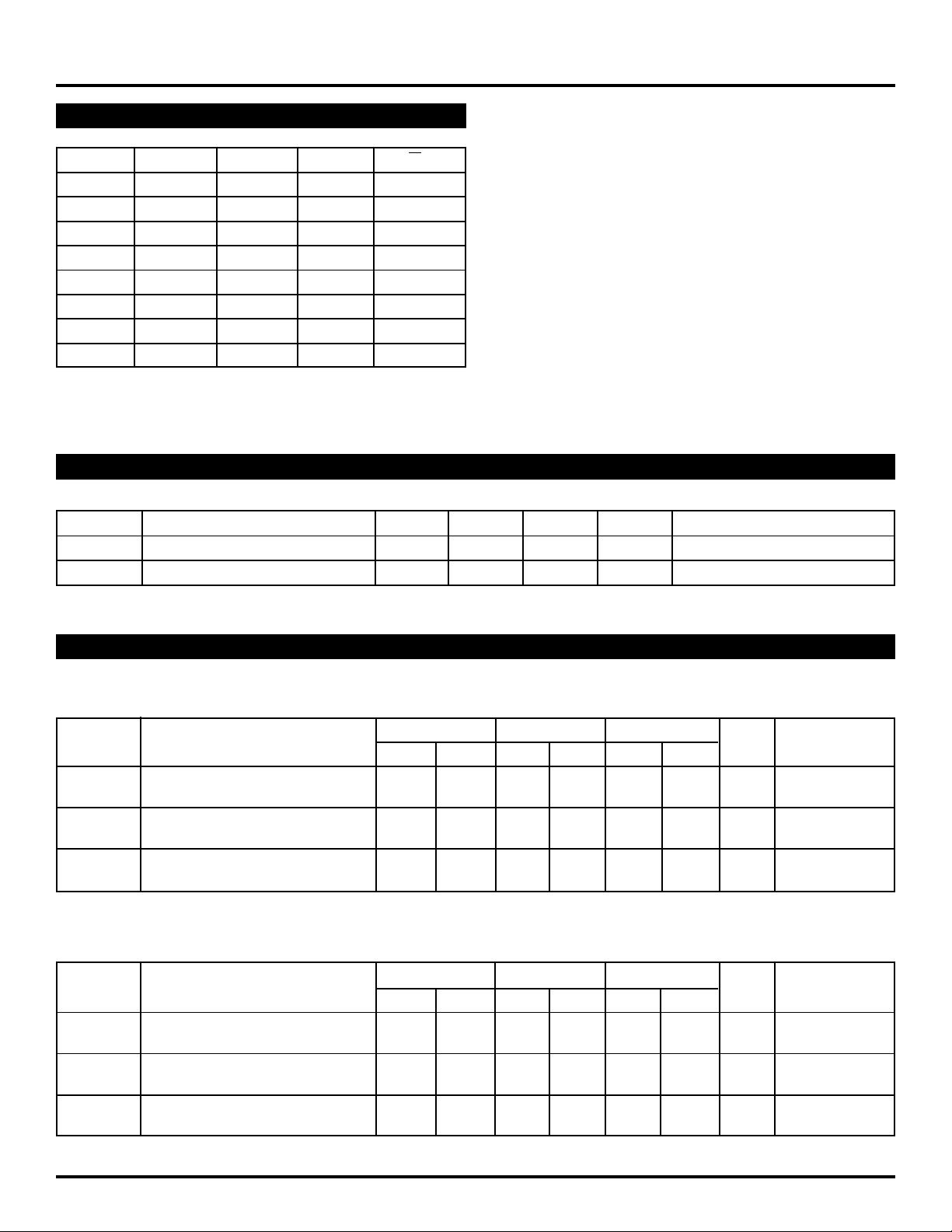
Top View
Flatpack
F24-1
V
CC
V
CCA
O
d
O
c
O
d
O
c
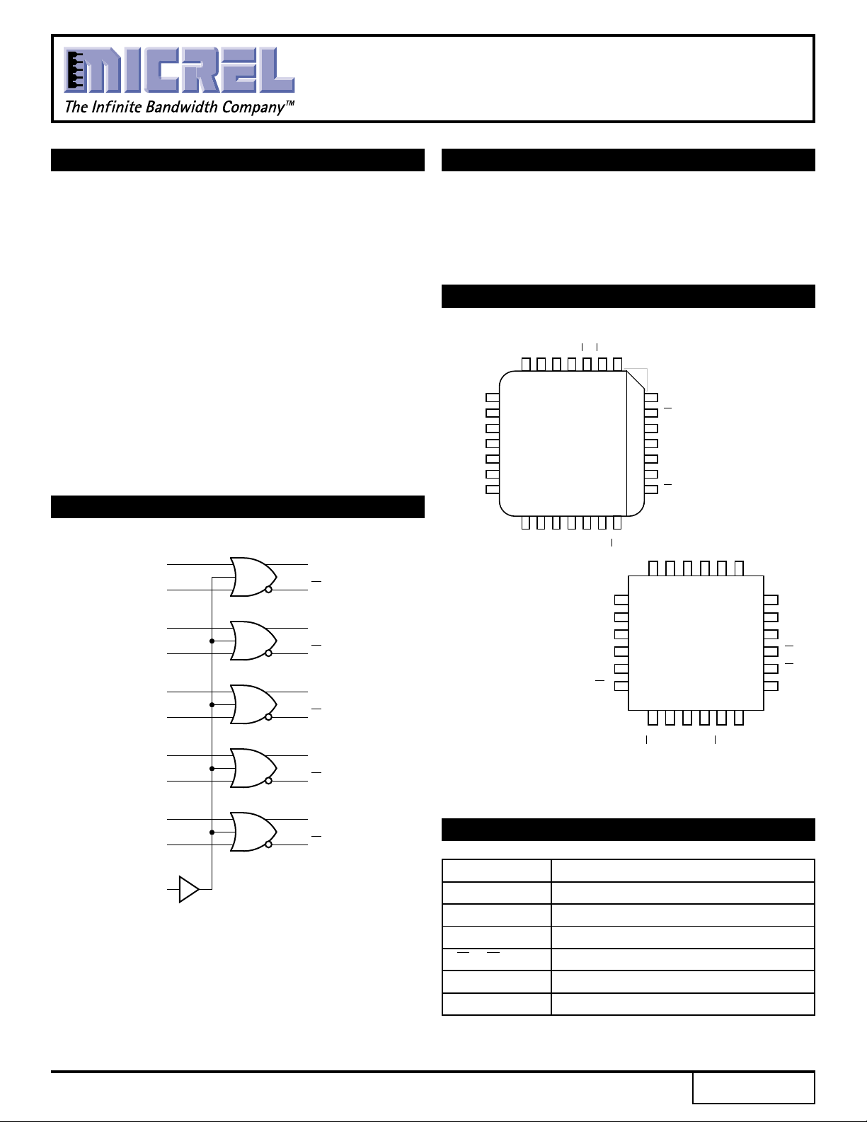
OR/NOR GATE
SY100S302
FEATURES
■ Max. propagation delay of 700ps
■ IEE min. of –45mA
■ Industry standard 100K ECL levels
■ Extended supply voltage option:
VEE = –4.2V to –5.5V
■ Voltage and temperature compensation for
improved noise immunity
■ Internal 75KΩ input pull-down resistors
■ 50% faster than Fairchild 300K
■ Function and pinout compatible with Fairchild F100K
■ Available in 24-pin CERPACK and 28-pin PLCC
packages
BLOCK DIAGRAM
O
D
1a
a
DESCRIPTION
The SY100S302 offers five 2-input OR/NOR gates
designed for use in high-performance ECL systems. The
five gates are controlled by a common Enable signal. All
inputs have 75KΩ pull-down resistors and all outputs are
buffered.
PIN CONFIGURATIONS
D2a
D1a
Oa
OaObOb
VEES
5
6
D1b
D
VEE
VEES
D1c
12
2b
13
14
15
E
16
17
Top View
PLCC
J28-1
1911201021922823724
D1e
D2d
D1d
VEES
D2e
25
Oe
Oc
4
3
Oc
VCCA
2
1
VCC
VCC
28
27
Od
2618
Oe
dD2c
O
D
D
D
D
D
D
D
D
D
2a
1b
2b
1c
2c
1d
2d
1e
O
a
O
b
O
b
O
c
O
c
O
d
O
d
O
e
D
1d
D
1e
O
e
18
D
2a
PIN NAMES
2e
E
O
e
Pin Function
Dna – Dne Data Inputs (n-1...5)
E Enable Input
Oa – Oe Data Outputs
Oa – Oe Complementary Data Outputs
VEES VEE Substrate
V
CCA VCCO for ECL Outputs
1
Rev.: G Amendment: /0
Issue Date: July, 1999
Micrel
SY100S302
TRUTH TABLE
D1X D2X E OX OX
L LLL H
LLHHL
LHLHL
L HHH L
HLLHL
HLHHL
HHLHL
H HHH L
NOTE:
1. H = High Voltage Level
L = Low Voltage Level
(1)
DC ELECTRICAL CHARACTERISTICS
VEE = –4.2V to –5.5V unless otherwise specified, VCC = VCCA = GND
Symbol Parameter Min. Typ. Max. Unit Condition
IIH Input HIGH Current, All Inputs — — 200 µAVIN = VIH (Max.)
EE Power Supply Current –45 –28 –21 mA Inputs Open
I
AC ELECTRICAL CHARACTERISTICS
CERPACK
VEE = –4.2V to –5.5V unless otherwise specified, VCC = VCCA = GND
TA = 0°CTA = +25°CTA = +85°C
Symbol Parameter Min. Max. Min. Max. Min. Max. Unit Condition
t
PLH Propagation Delay 300 750 300 750 300 750 ps
tPHL Data to Output
PLH Propogation Delay 250 950 250 950 250 950 ps
t
tPHL Enable to Output
TLH Transition Time 300 900 300 900 300 900 ps
t
tTHL 20% to 80%, 80% to 20%
PLCC
VEE = –4.2V to –5.5V unless otherwise specified, VCC = VCCA = GND
TA = 0°CTA = +25°CTA = +85°C
Symbol Parameter Min. Max. Min. Max. Min. Max. Unit Condition
PLH Propagation Delay 250 700 250 700 250 700 ps
t
tPHL Data to Output
PLH Propogation Delay 250 900 250 900 250 900 ps
t
tPHL Enable to Output
t
TLH Transition Time 300 900 300 900 300 900 ps
tTHL 20% to 80%, 80% to 20%
2
 Loading...