

MICREL SY100S301 Datasheet
TRIPLE 5-INPUT
D4bD3bD
2b
V
EE
D1bD
5a
D
3a
D
2a
D
1a
O
a
D
1c
D
5c
D
3c
17
16
15
14
13
1
2
3
4
5
6
7248239221021112012
19
Top View
Flatpack
F24-1
O
a
V
CC
V
CCA
O
b
OcO
c
O
b
OR/NOR GATE
SY100S301
FEATURES
■ Max. propagation delay of 750ps
■ I
EE min. of –25mA
■ Industry standard 100K ECL levels
■ Extended supply voltage option:
VEE = –4.2V to –5.5V
■ Voltage and temperature compensation for
improved noise immunity
■ 20% faster than Fairchild 300K at lower power
■ Internal 75KΩ input pull-down resistors
■ Function and pinout compatible with Fairchild F100K
■ Available in 24-pin CERPACK and 28-pin PLCC
packages
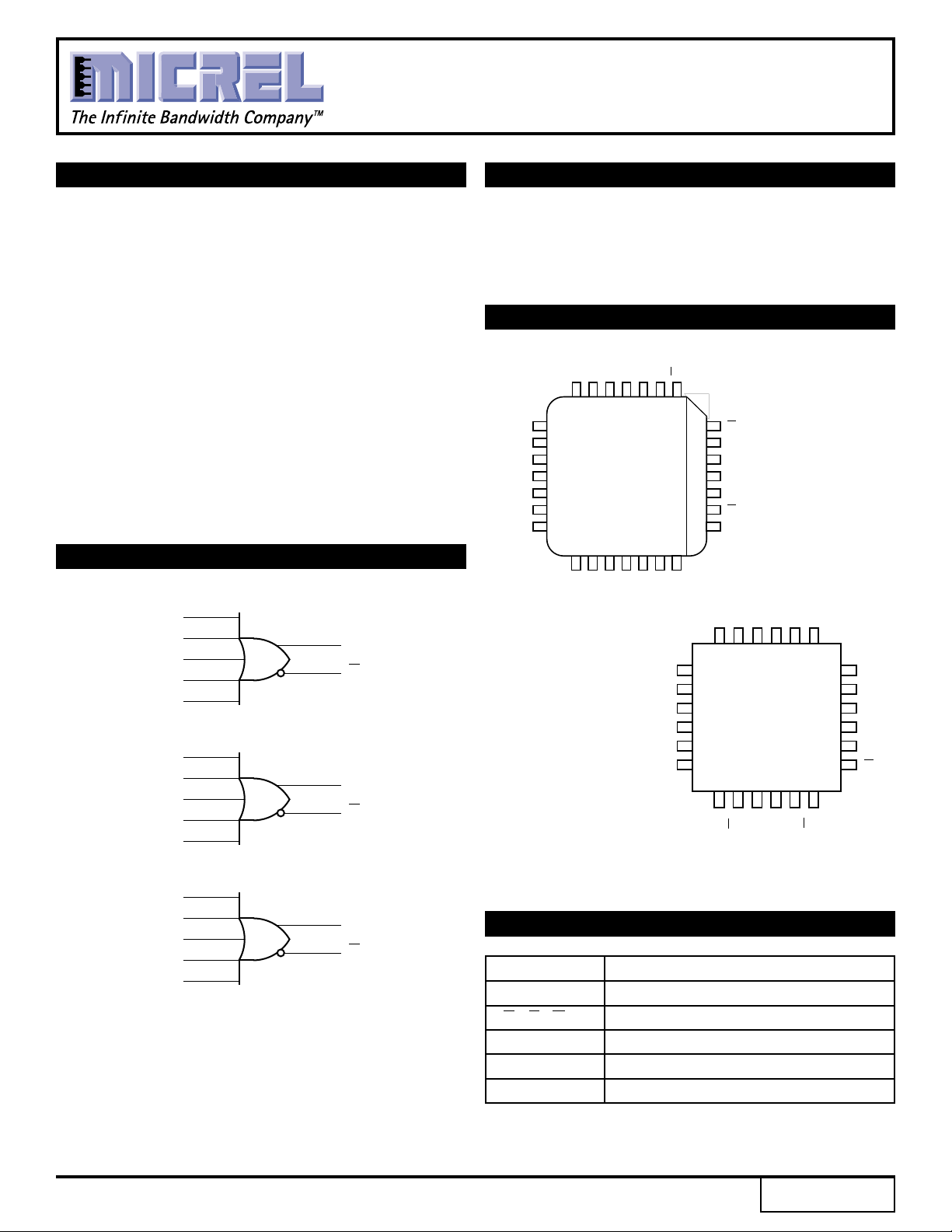
BLOCK DIAGRAM
D
1a
D
2a
D
3a
D
4a
D
5a
O
a
O
a
DESCRIPTION
The SY100S301 is an ultra-fast triple 5-input OR/NOR
gate designed for use in high-performance ECL systems.
The inputs on this device have 75KΩ pull-down resistors.
PIN CONFIGURATIONS
D4a
D3a
D2a
VEESD1a
Oa
Oa
6
5
D5a
D1b
VEE
VEES
D2b
D3b
12
13
14
15
16
17
Top View
PLCC
J28-1
1911201021922823724
D2c
D1c
D5b
VEES
25
D3c
D4c
D
5b
D
2c
Ob
4
3
Ob
2
VCCA
1
VCC
28
VCC
27
Oc
2618
O
cD4b
D5c
18
D
4a
D
D
D
D
D
D
D
D
D
D
D
1b
2b
3b
4b
5b
1c
2c
3c
4c
5c
O
b
O
b
O
c
O
c
PIN NAMES
Pin Function
Dna, Dnb, Dnc Data Inputs (n-1...5)
4c
Oa, Ob, Oc Data Outputs
Oa, Ob, Oc Complementary Data Outputs
VEES VEE Substrate
V
CCA VCCO for ECL Outputs
Rev.: F Amendment: /0
1
Issue Date: July, 1999
Micrel
SY100S301
LOGIC EQUATION
Oa = D1a + D2a + D3a + D4a + D5a
Ob = D1b + D2b + D3b + D4a + D5b
Oc = D1c + D2c + D3c + D4c + D5c
GUARANTEED OPERATING CONDITIONS
Symbol Parameter Min. Typ. Max. Unit
VEE Input HIGH Current –5.5 –4.5 –4.2 V
A Power Supply Current 0 25 85 ˚C
T
ABSOLUTE MAXIMUM RATINGS
Symbol Rating Value Unit
VEE Power Supply –0.5 to +7.0 V
VIN Input Voltage –0.5 to VEE V
IOUT DC Output Current –50 mA
TC Temperature Under Bias –55 to +125 ˚C
TJ Junction Temperature +150 ˚C
store Storage Temperature –65 to +150 ˚C
T
NOTE:
1. Permanent device damage may occur if ABSOLUTE MAXIMUM RATINGS
are exceeded. This is a stress rating only and functional operation is not
implied at conditions other than those detailed in the operational sections
of this data book. Exposure to ABSOLUTE MAXIMUM RATING conditions
for extended periods may affect device reliability.
(1)
DC ELECTRICAL CHARACTERISTICS
VEE = –4.2V to –5.5V unless otherwise specified, VCC = VCCA = GND
Symbol Parameter Min. Typ. Max. Unit Condition
IIH Input HIGH Current — — 200 µA—
EE Power Supply Current –25 –17 –11 mA Inputs Open
I
AC ELECTRICAL CHARACTERISTICS
CERPACK
VEE = –4.2V to –5.5V unless otherwise specified, VCC = VCCA = GND
TA = 0°CTA = +25°CTA = +85°C
Symbol Parameter Min. Max. Min. Max. Min. Max. Unit Condition
PLH Propagation Delay 300 800 300 800 300 800 ps
t
tPHL Data to Output
TLH Transition Time 300 900 300 900 300 900 ps
t
tTHL 20% to 80%, 80% to 20%
PLCC
VEE = –4.2V to –5.5V unless otherwise specified, VCC = VCCA = GND
TA = 0°CTA = +25°CTA = +85°C
Symbol Parameter Min. Max. Min. Max. Min. Max. Unit Condition
PLH Propagation Delay 300 750 300 750 300 750 ps
t
tPHL Data to Output
t
TLH Transition Time 300 900 300 900 300 900 ps
tTHL 20% to 80%, 80% to 20%
2
 Loading...