

MICREL SY10H646L, SY100H646L Datasheet
3.3V SINGLE SUPPLY
OCTAL PECL/TTL-TO-TTL
ClockWorks™
SY10H646L
SY100H646L
FEATURES
■ 3.3V power supply
■ PECL/TTL-to-TTL version of popular ECLinPS
E111AE/LE
■ Guaranteed low skew specification
■ Three-state enable
■ Differential internal design
■ VBB output for single-ended operation
■ Extra TTL and ECL power/ground pins
■ Choice of ECL compatibility: 10K or 100K
■ Matched high and low output impedance
■ Available in 28-pin PLCC package
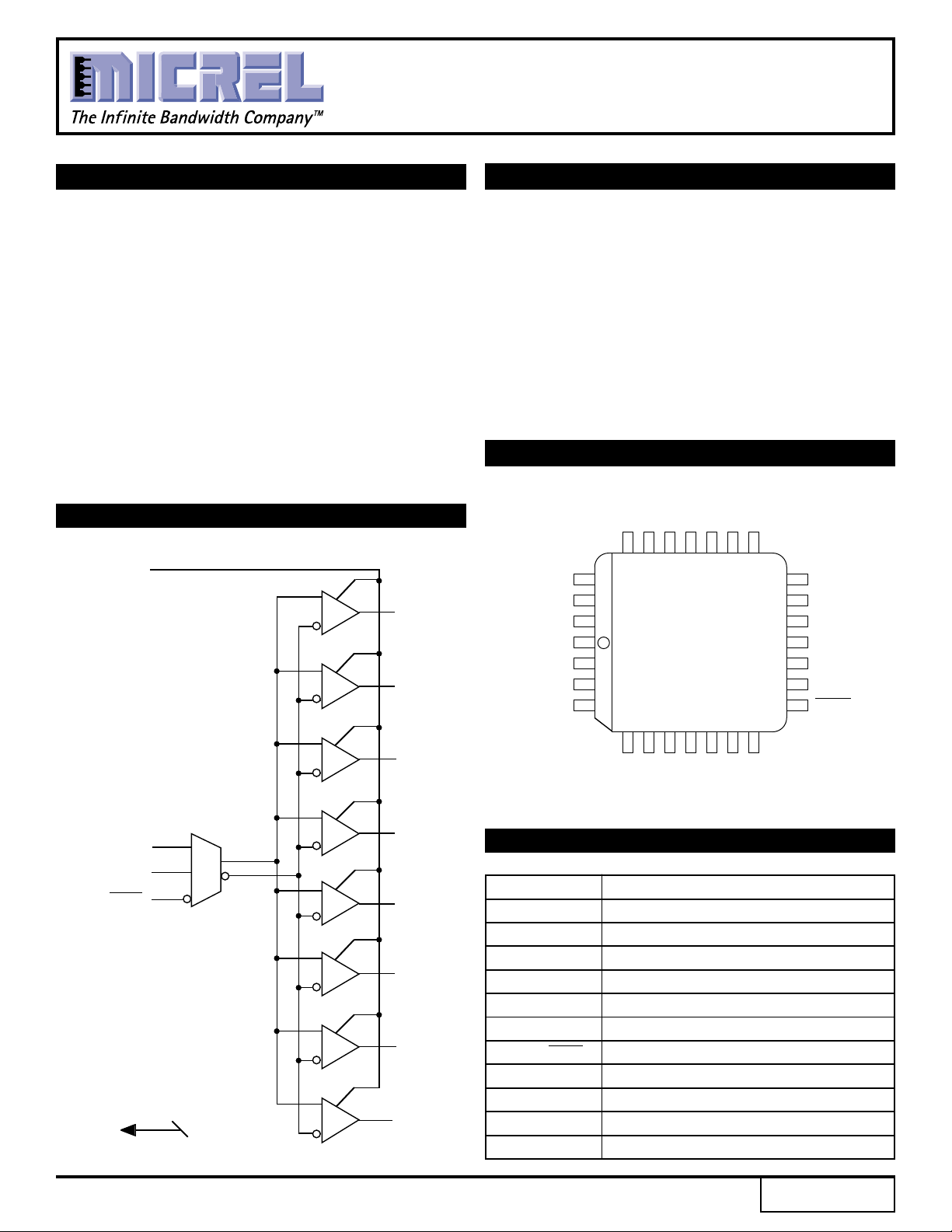
BLOCK DIAGRAM
EN
Q
Q
DESCRIPTION
The SY10/100H646L are single supply, low skew
translating 1:8 clock drivers. Devices in the MicrelSynergy H600 translator series utilize the 28-lead PLCC
for optimal power pinning, signal flow-through and
electrical performance. The single supply H646L is similar
to the HA643 which is a dual supply 1:8 version of the
same function.
These devices feature a 24mA TTL output stage, with
AC performance specified into a 20pF load capacitance.
The 10H version is compatible with 10K ECL logic
levels. The 100H version is compatible with 100K levels.
PIN CONFIGURATION
Q5
Q4OGND
25
24 23 22 21 20 19
Q3
0
OGND
Q
OVT
Q
1
OGND
Q
26
27
2
28
1
1
2
3
0
4
567891011
OVT
TOP VIEW
PLCC
7
Q6OGND
Q
18
EN
17
IVT
16
IGND
15
VCCE
14
VCCE
13
VBB
12
ECLK
TCLK
ECLK
ECLK
V
BB
Q
2
TCLK
Q
3
PIN NAMES
IVT
EE
V
IGND
VEE
VEE
ECLK
Pin Function
Q
4
OGND TTL Output Ground (0V)
OVT TTL Output VCC (+3.0V)
IGND Internal TTL GND (0V)
Q
5
IVT Internal TTL VCC (+3.0V)
VEE ECL VEE (0V)
VCCE ECL Ground (+3.0V)
Q
6
ECLK, ECLK Differential Signal Input (PECL)
VBB VBB Reference Output
Q0–Q7 Signal Outputs (TTL)
Q
7
EN Three-State Enable Input (TTL)
TCLK Signal Input (TTL)
1
Rev.: E Amendment: /0
Issue Date: May, 1999
ClockWorks™
SY10H646L
SY100H646LMicrel
ABSOLUTE MAXIMUM RATINGS
(1)
Symbol Rating Value Unit
E (ECL) Power Supply –0.5 to +7.0 V
V
VT (TTL) Voltage –0.5 to +7.0
VI (ECL) Input Voltage 0.0 to VEE V
VI (TTL) –0.5 to VCC
VOUT (TTL) Disabled 3-State 0.0 to VCCT V
Output
I
OUT (ECL) Output Current mA
- Continuous 50
- Surge 100
Tstore Storage Temperature –65 to +150 ˚C
T
A Operating Temperature 0 to +85 ˚C
NOTE:
1. Do not exceed.
TRUTH TABLE
TCLK ECLK ECLK EN Q
GND L H H L
GND H L H H
H GND GND H H
L GND GND H L
XX XL Z
NOTE:
X = Don't Care
L = Low Voltage Level
H = High Voltage Level
Z = Three-State
DC ELECTRICAL CHARACTERISTICS
OVT = IVT = VCCE = 3.0V to 3.6V
TA = 0°CTA = +25°CTA = +85°C
Symbol Parameter Min. Max. Min. Max. Min. Max. Unit Condition
CCL Power Supply Current — 120 — 120 — 120 mA Total all OVT,
I
ICCH — 120 — 120 — 120 IVT, and VCCE pins
TTL DC ELECTRICAL CHARACTERISTICS
OVT = IVT = VCCE = 3.0V to 3.6V
TA = 0°CTA = +25°CTA = +85°C
Symbol Parameter Min. Max. Min. Max. Min. Max. Unit Condition
VIH Input HIGH Voltage 2.0 — 2.0 — 2.0 — V
VIL Input LOW Voltage — 0.8 — 0.8 — 0.8 V
I
IH Input HIGH Current — 20 — 20 — 20 µAVIN = 2.7 V
— 100 — 100 — 100 VIN = VCC
IIL Input LOW Current —–0.4 —–0.4 —–0.4 mA VIN = 0.5 V
VOH Output HIGH Voltage 2.0 — 2.0 — 2.0 — VIOH = –3.0 mA
VOL Output LOW Voltage — 0.5 — 0.5 — 0.5 V IOL = 24 mA
VIK Input Clamp Voltage —–1.2 —–1.2 —–1.2 V IIN = –18mA
OS Output Short Circuit Current –100 —–100 —–100 — mA VOH = 0V
I
2
 Loading...