

MICREL SY10H641, SY100H641 Datasheet
SINGLE SUPPLY 1:9
PECL-TO-TTL
ClockWorks™
SY10H641
SY100H641
FEATURES
■ Input frequencies up to 135MHz
■ PECL-to-TTL version of popular ECLinPS E111
■ Guaranteed low skew specification
■ Latched input
■ Differential internal design
■ V
BB output VECL for single-ended operation
■ Single +5V supply
■ Reset/enable
■ Extra TTL and ECL power/ground pins
■ Choice of ECL compatibility: MECL 10KH (10Hxxx)
or 100K (100Hxxx)
■ Available in 28-pin PLCC package
TTL Outputs
Q0
Q1
Q2
DESCRIPTION
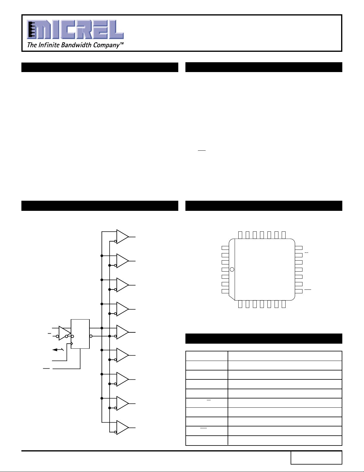
The SY10/100H641 are single supply, low skew
translating 1:9 clock drivers. Devices in the MicrelSynergy H600 translator series utilize the 28-lead PLCC
for optimal power pinning, signal flow-through and
electrical performance.
The devices feature a 24mA TTL output stage with
AC performance specified into a 50pF load capacitance.
A latch is provided on-chip. When LEN is LOW (or left
open, in which case it is pulled LOW by the internal pulldowns), the latch is transparent. A HIGH on the enable
pin (EN) forces all outputs LOW.
The 10H version is compatible with MECL 10KH ECL
logic levels. The 100H version is compatible with 100K
levels.
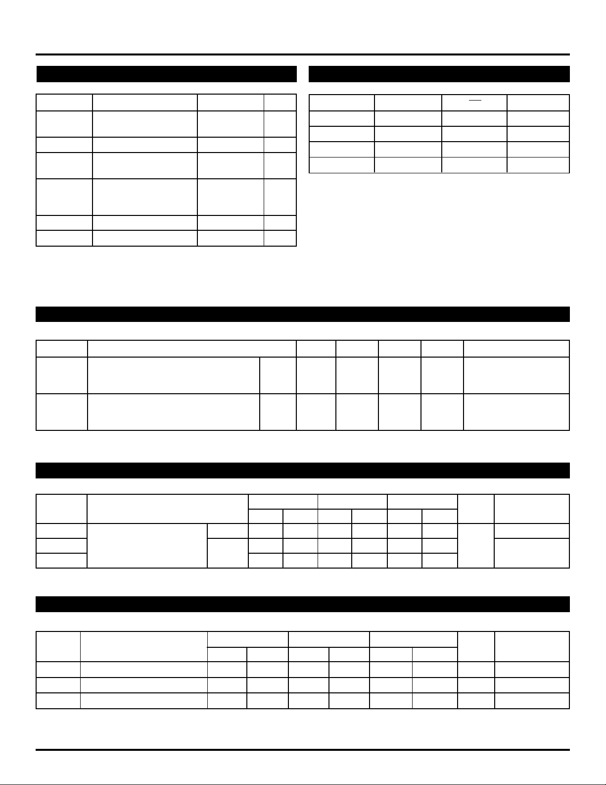
PIN CONFIGURATIONBLOCK DIAGRAM
7
6
T
T
Q
G
V
25 24 23 22 21 20 19
26
G
T
27
Q
5
28
V
T
1
Q
4
2
V
T
3
Q
3
4
G
T
TOP VIEW
PLCC
567891011
8
T
T
Q
Q
G
V
18
V
BB
17
D
16
D
15
V
E
14
LEN
13
12
G
EN
E
PECL Input
D
D
VBB
LEN
EN
Q3
Q
D
Q4
2
T
Q
G
T
T
1
V
Q
T
0
V
G
Q
PIN NAMES
Q5
Q6
Q7
Q8
1
Pin Function
GT TTL Ground (0V)
VT TTL VCC (+5.0V)
VE ECL VCC (+5.0V)
GE ECL Ground (0V)
D, D Signal Input (PECL)
VBB VBB Reference Output (PECL)
Q0 - Q8 Signal Outputs (TTL)
EN Enable Input (PECL)
LEN Latch Enable Input (PECL)
Rev.: D Amendment: /0
Issue Date: March, 1999
Micrel
ClockWorks™
SY10H641
SY100H641
ABSOLUTE MAXIMUM RATINGS
(1)
Symbol Rating Value Unit
E (ECL) Power Supply –0.5 to +7.0 V
V
VT (TTL) Voltage –0.5 to +7.0
VI (ECL) Input Voltage 0.0 to VEE V
OUT (TTL) Disabled 3-State 0.0 to VCCT V
V
Output
I
OUT (ECL) Output Current mA
TRUTH TABLE
D LEN EN Q
LL LL
HL LH
XH LQ0
XX HL
- Continuous 50
- Surge 100
Tstore Storage Temperature –65 to +150 ˚C
T
A Operating Temperature 0 to +85 ˚C
NOTE:
1. Do not exceed.
VCC AND CLOAD
Ranges to meet duty cycle requirement: 0°C ≤ TA ≤ 85°C. Output duty cycle measured relative to 1.5V.
Symbol Parameter Min. Typ. Max. Unit Condition
W1 Ranges of VCC and CL to meet min. VCC 4.75 5.0 5.25 V All Outputs
P
pulse width (HIGH or LOW) at CL 10 — 50 pF
fOUT ≤ 40MHz PW 11 — — ns
W2 Ranges of VCC and CL to meet min. VCC 4.875 5.0 5.125 V All Outputs
P
pulse width (HIGH or LOW) at CL 15 — 27 pF
fOUT ≤ 50MHz PW 9.0 — — ns
DC ELECTRICAL CHARACTERISTICS
VT = VE = 5.0V ± 5%
TA = 0°CTA = +25°CTA = +85°C
Symbol Parameter Min. Max. Min. Max. Min. Max. Unit Condition
EE Power Supply Current ECL — 30 — 30 — 30 mA VE Pin
I
CCH TTL — 30 — 30 — 30 Total all VT pins
I
CCL —35—35—35
I
TTL DC ELECTRICAL CHARACTERISTICS
VT = VE = 5.0V ± 5%
TA = 0°CTA = +25°CTA = +85°C
Symbol Parameter Min. Max. Min. Max. Min. Max. Unit Condition
VOH Output HIGH Voltage 2.0 — 2.0 — 2.0 — V IOH = –15mA
VOL Output LOW Voltage — 0.5 — 0.5 — 0.5 V IOL = 24mA
OS Output Short Circuit Current –100 –225 –100 –225 –100 –225 mA VOUT = 0V
I
2
 Loading...