

MICREL SY10H603, SY100H603 Datasheet
9-BIT LATCHED
5
ECL-TO-TTL
SY10H603
SY100H603
FEATURES
■ 9-bit ideal for byte-parity applications
■ 3-state TTL outputs
■ Flow-through configuration
■ Extra TTL and ECL power/ground pins to minimize
switching noise
■ Dual supply
■ 6.0ns max. delay into 50pF, 12ns into 200pF (all
outputs switching)
■ PNP TTL inputs for low loading
■ Choice of ECL compatibility: MECL 10KH (10Hxxx)
or 100K (100Hxxx)
■ Fully compatible with Motorola MC10H/100H603
■ Available in 28-pin PLCC package
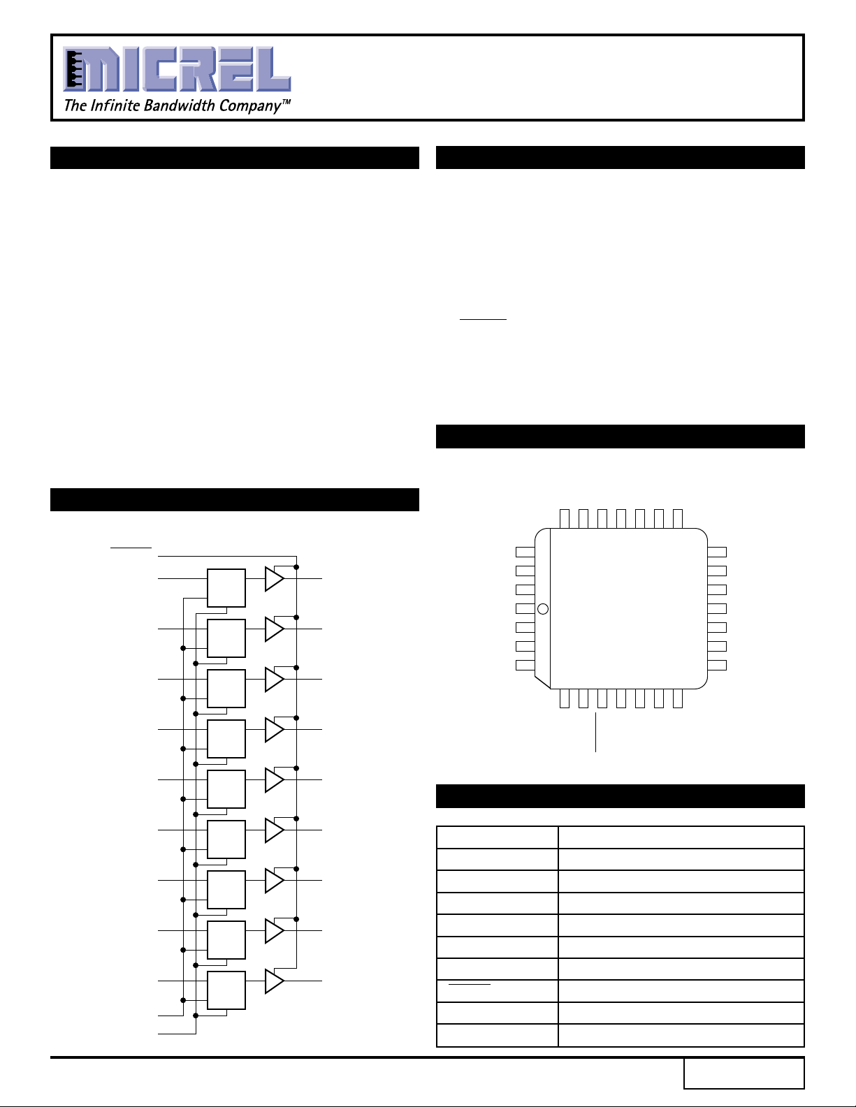
BLOCK DIAGRAM
OEECL
Q
D
0
QD
EN
D
1
QD
EN
D
2
QD
EN
D
3
QD
EN
0
Q
1
Q
2
Q
3
DESCRIPTION
The SY10/100H603 are 9-bit, dual supply ECL-to-TTL
translators. Devices in the Micrel-Synergy 9-bit translator
series utilize the 28-lead PLCC for optimal power pinning,
signal flow-through and electrical performance.
The devices feature a 48mA TTL output stage and AC
performance is specified into both a 50pF and 200pF
load capacitance. Latching is controlled by Latch Enable
(LEN) and Master Reset (MR) resets the latches. A HIGH
on OEECL sends the outputs into the high impedance
state. All control inputs are ECL level.
The 10H version is compatible with MECL 10KH ECL
logic levels. The 100H version is compatible with 100K
levels.
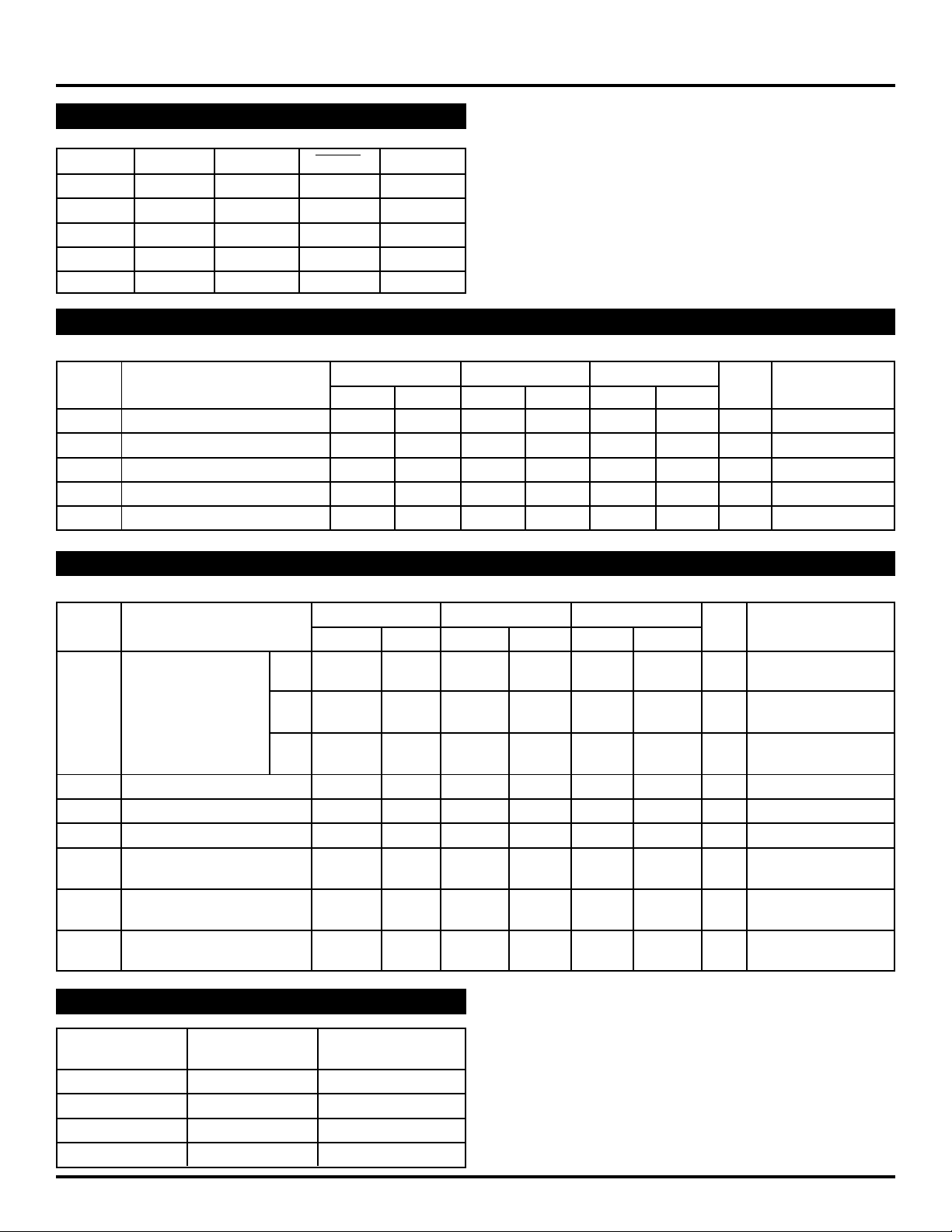
PIN CONFIGURATION
7
GND
D0
8
Q
Q
18
D8
17
D7
16
VCCE
15
D6
14
D5
13
D4
12
D3
D2
D1
Q4
Q3
VCCT
Q2
GND
Q
Q0
VCCT
GND
Q5
25 24 23 22 21 20 19
26
27
28
1
2
3
1
4
567891011
MR
Q6
TOP VIEW
PLCC
EE
V
LEN
OEECL
ECL
D
4
QD
EN
D
QD
EN
D
6
QD
EN
D
7
QD
EN
Q
4
TTL
PIN NAMES
Q
5
Q
6
Q
7
Pin Function
GND TTL Ground (0V)
VCCE ECL VCC (0V)
VCCT TTL Supply (+5.0V)
VEE ECL Supply (–5.2/–4.5V)
D0–D8 Data Inputs (ECL)
Q0–Q8 Data Outputs (TTL)
Q
D
8
QD
EN
LEN
MR
8
OEECL 3-state Control (ECL)
LEN Latch Enable (ECL)
MR Master Reset (ECL)
Rev.: D Amendment: /0
1
Issue Date: April, 1998
SY10H603
Micrel
SY100H603
LOGIC DIAGRAMTRUTH TABLE
D LEN MR OEECL Q
LLLLL
HLLLH
XHLLQ0
XXHLL
XXXHZ
DC ELECTRICAL CHARACTERISTICS
VCCT = 5.0V ± 10%; VEE = –4.75V to –5.5V (10H Version); VEE = –4.2V to –5.5V (100H Version)
TA = 0°CTA = +25°CTA = +85°C
Symbol Parameter Min. Max. Min. Max. Min. Max. Unit Condition
IEE Power Supply Current, ECL 45 63 45 64 45 68 mA —
ICC Power Supply Current, TTL 80 110 80 110 80 110 mA —
IOS Output Short Circuit Current –100 –225 –100 –225 –100 –225 mA VOUT = 0V
IOZH Output Disable Current, HIGH — 50 — 50 — 50 µAVOUT = 2.7V
OZL Output Disable Current, LOW —–50 —–50 —–50 µAVOUT = 0.5V
I
LOGIC DIAGRAMAC ELECTRICAL CHARACTERISTICS
VCCT = 5.0V ± 10%; VEE = –4.75V to –5.5V (10H Version); VEE = –4.2V to –5.5V (100H Version)
TA = 0°CTA = +25°CTA = +85°C
Symbol Parameter Min. Max. Min. Max. Min. Max. Unit Condition
PLH Propagation Delay D 3.2 6.0 3.2 6.0 3.2 6.0 ns CL = 50pF
t
tPHL to Output 6.4 12 6.4 12 6.4 12 CL = 200pF
LEN 3.5 6.5 3.5 6.5 3.5 6.5 ns C
7.0 13 7.0 13 7.0 13 CL = 200pF
MR 3.0 6.0 3.0 6.0 3.0 6.0 ns C
6.0 12 6.0 12 6.0 12 CL = 200pF
tS Set-up Time, D to LEN 1.5 — 1.5 — 1.5 — ns —
tH Hold Time, D to LEN 0.8 — 0.8 — 0.8 — ns —
(L)
tw
PLZ Output Disable Time 2.5 6.5 2.5 6.5 2.5 6.5 ns CL = 50pF
t
LEN Pulse Width, LOW 2.0 — 2.0 — 2.0 — ns —
tPHZ 4.2 13 4.2 13 4.2 13 CL = 200pF
PZL Output Enable Time 2.0 5.0 2.0 5.0 2.0 5.0 ns CL = 50pF
t
tPZH 4.0 10 4.0 10 4.0 10 CL = 200pF
r Output Rise/Fall Time 0.2 1.2 0.2 1.2 0.2 1.2 ns CL = 50pF
t
tf 1.0V – 2.0V 0.2 3.0 0.2 3.0 0.2 3.0 CL = 200pF
L = 50pF
L = 50pF
PRODUCT ORDERING CODE
Ordering Package Operating
Code Type Range
SY10H603JC J28-1 Commercial
SY10H603JCTR J28-1 Commercial
SY100H603JC J28-1 Commercial
SY100H603JCTR J28-1 Commercial
2
 Loading...