

MICREL SY10ELT21, SY100ELT21 Datasheet
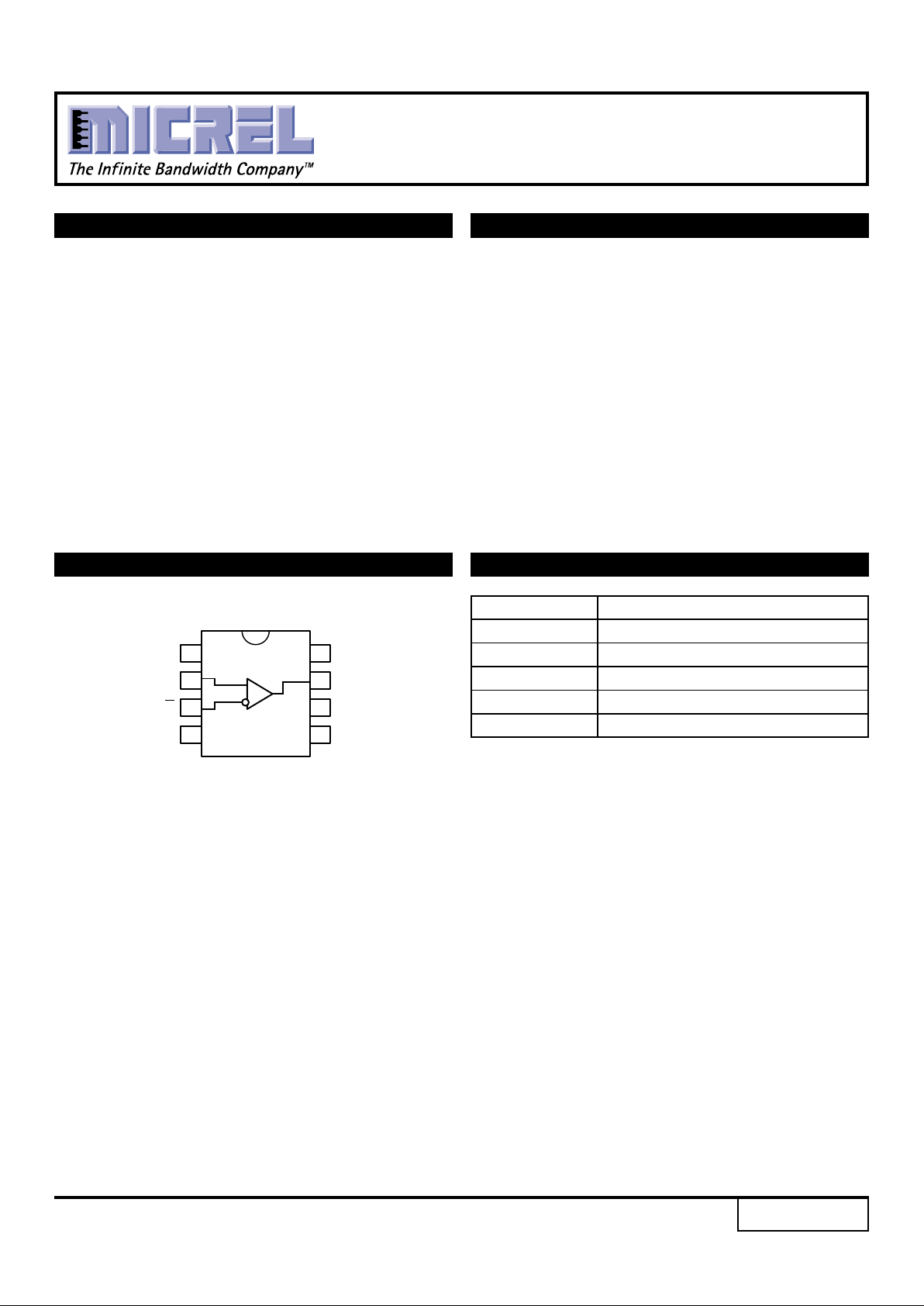
Pin Function
Q TTL Output
D, /D Differential PECL Inputs
V
CC
+5.0V Supply
V
BB
Reference Output
GND Ground
DESCRIPTION
■ 2.5ns typical propagation delay
■ Low power
■ Differential PECL inputs
■ 24mA TTL outputs
■ Flow-through pinouts
■ Available in 8-pin SOIC package
The SY10/100ELT21 are single differential PECL-toTTL translators. Because PECL (Positive ECL) levels are
used, only +5V and ground are required. The small outline
8-lead SOIC package and low skew single gate design
make the ELT21 ideal for applications that require the
translation of a clock or data signal where minimal space,
low power, and low cost are critical.
The V
BB
output allow differential single-ended, or ACcoupled interface to the device. If used, the VBB output
should be bypassed to VCC with a 0.01µF capacitor.
The ELT21 is available in both ECL standards: the
10ELT is compatible with positive ECL 10H logic levels,
while the 100ELT is compatible with positive ECL 100K
logic levels.
FEATURES
DIFFERENTIAL
PECL-to-TTL
TRANSLATOR
PIN NAMES
PIN CONFIGURATION/BLOCK DIAGRAM
SOIC
TOP VIEW
ClockWorks™
SY10ELT21
SY100ELT21
1NC
D
D
V
BB
8V
CC
Q
NC
GND
7
6
5
2
3
4
PECL
TTL
1
Rev.: B Amendment: /0
Issue Date:
April 2000
2
ClockWorks™
SY10ELT21
SY100ELT21
Micrel
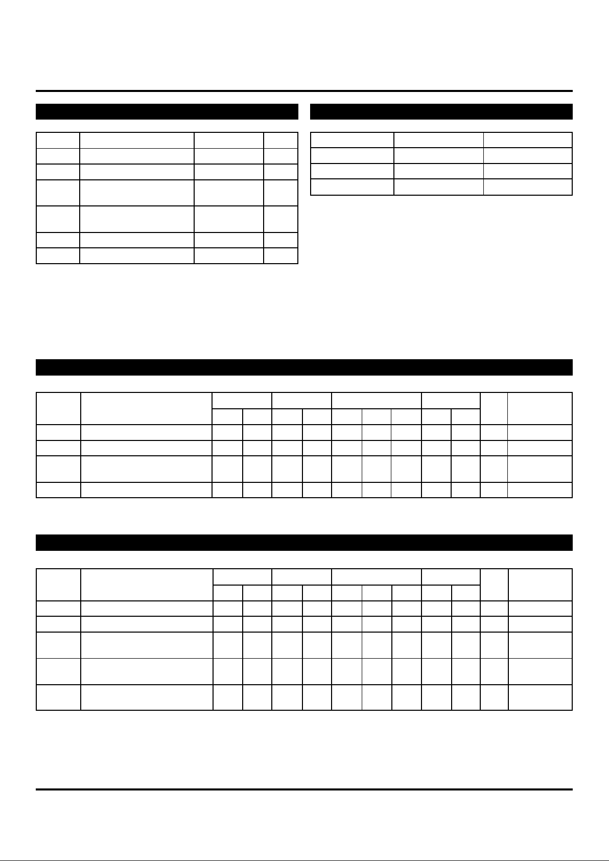
Symbol Parameter Value Unit
V
CC
Power Supply Voltage –0.5 to +7.0 V
V
I
PECL Input Voltage 0V to VCC+0.5 V
V
O
Voltage Applied to –0.5 to +5.5 V
Output at HIGH State
I
O
Current Applied to Twice the mA
Output at LOW State Rated I
OL
T
store
Storage Temperature –65 to +150 °C
T
A
Operating Temperature –40 to +85 °C
NOTE:
1. Permanent device damage may occur if ABSOLUTE MAXIMUM RATINGS
are exceeded. This is a stress rating only and functional operation is not
implied at conditions other than those detailed in the operational sections
of this data sheet. Exposure to ABSOLUTE MAXIMUM RATlNG conditions
for extended periods may affect device reliability.
ABSOLUTE MAXIMUM RATINGS
(1)
TRUTH TABLE
D/D Q
LH L
HL H
Open Open L
TA = –40°CTA = 0°CTA = +25°CTA = +85°C
Symbol Parameter Min. Max. Min. Max. Min. Typ. Max. Min. Max. Unit Condition
I
OS
Output Short Circuit Current –80 –200 –80 –200 –80 — –200 –80 –200 mA V
OUT
= 0V
I
CC
Power Supply Current — 20 — 20 — 14 20 — 20 mA —
V
OH
Output HIGH Voltage 2.5 — 2.5 — 2.5 — — 2.5 — V IOH = –3.0mA
2.0 — 2.0 — 2.0 — — 2.0 — V IOH = –15mA
V
OL
Output LOW Voltage — 0.5 — 0.5 — — 0.5 — 0.5 V IOL = 24mA
TTL DC ELECTRICAL CHARACTERISTICS
VCC = 4.75V to 5.25V
TA = –40°CTA = 0°CTA = +25°CTA = +85°C
Symbol Parameter Min. Max. Min. Max. Min. Typ. Max. Min. Max. Unit Condition
I
IH
Input HIGH Current — 150 — 150 — — 150 — 150 µA
I
IL
Input LOW Current 0.5 — 0.5 — 0.5 — — 0.5 — µA
V
IH
Input HIGH Voltage
(2)
10ELT 3770 4110 3830 4160 3870 — 4190 3940 4280 mV
100ELT 3835 4120 3835 4120 3835 4120 3835 4120
V
IL
Input LOW Voltage
(2)
10ELT 3050 3500 3050 3520 3050 — 3520 3050 3555 mV
100ELT 3190 3525 3190 3525 3190 — 3525 3190 3525
V
BB
Reference Output
(2)
10ELT 3570 3700 3620 3730 3650 — 3750 3690 3810 mV
100ELT 3620 3740 3620 3740 3620 — 3740 3620 3740
PECL DC ELECTRICAL CHARACTERISTICS
VCC = 4.75V to 5.25V
NOTES:
1. These values are for VCC = 5.0V. Level Specifications will vary 1:1 VCC.
 Loading...