

MICREL SY10ELT20V, SY100ELT20V Datasheet

5V/3.3V
TTL-to-DIFFERENTIAL
PECL TRANSLA TOR
ClockWorks™
SY10ELT20V
SY100ELT20V
FEATURES
■ 3.3V and 5V power supply options
■ 300ps typical propagation delay
■ Low power
■ Differential PECL output
■ PNP TTL input for minimal loading
■ Flow-through pinouts
■ Available in 8-pin SOIC package
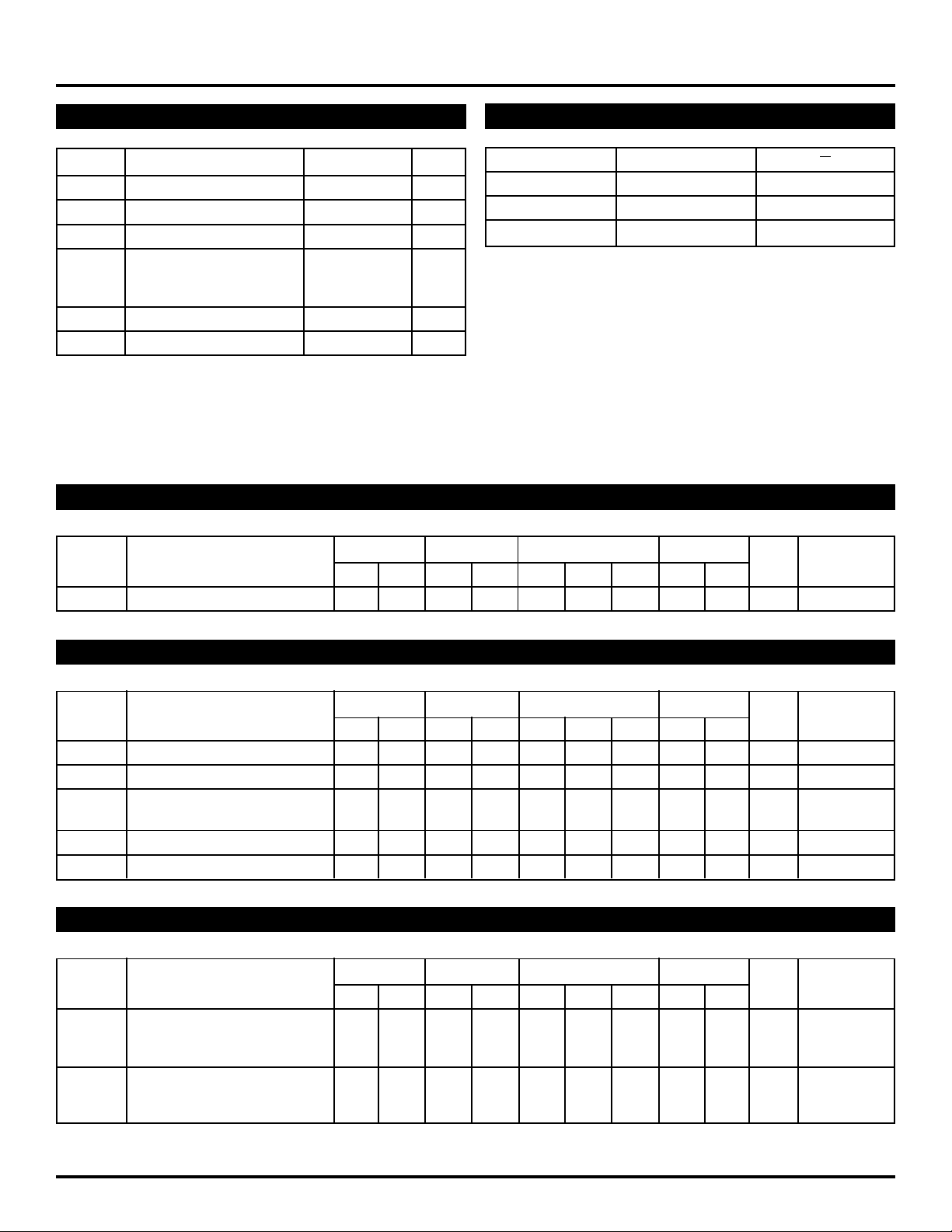
PIN CONFIGURATION/BLOCK DIAGRAM
NC
1NC
2
Q
PECL
3
Q
4
TTL
8V
CC
D
7
NC
6
GND
5
DESCRIPTION
The SY10/100ELT20V is a single TTL-to-differential
PECL translators. Because PECL (Positive ECL) levels
are used, either +5V or +3.3V and ground are required.
The small outline 8-lead SOIC package and low skew
single gate design make the ELT20V ideal for applications
that require the translation of a clock or data signal where
minimal space, low power, and low cost are critical.
The ELT20V is available in both ECL standards: the
10ELT is compatible with positive ECL 10H logic levels,
while the 100ELT is compatible with positive ECL 100K
logic levels.
PIN NAMES
Pin Function
Q Differential PECL Output
D TTL Input
VCC +5V/+3.3V Supply
GND Ground
SOIC
TOP VIEW
Rev.: A Amendment: /0
1
Issue Date:
December 1999
Micrel
ClockWorks™
SY10ELT20V
SY100ELT20V
ABSOLUTE MAXIMUM RATINGS
(1)
Symbol Paramter Value Unit
VCC Power Supply Voltage –0.5 to +7.0 V
VI TTL Input Voltage –0.5 to VCC V
II TTL Input Current –30 to +5.0 mA
OUT PECL Output Current mA
I
TRUTH TABLE
DQ Q
HH L
LL H
Open H L
–Continuous 50
–Surge 100
Tstore Storage Temperature –65 to +150 °C
A Operating Temperature –40 to +85 °C
T
NOTE:
1. Permanent device damage may occur if ABSOLUTE MAXIMUM RATINGS
are exceeded. This is a stress rating only and functional operation is not
implied at conditions other than those detailed in the operational sections
of this data sheet. Exposure to ABSOLUTE MAXIMUM RATlNG conditions
for extended periods may affect device reliability.
DC ELECTRICAL CHARACTERISTICS
VCC = +3.3V ±10% or +5.0V ±10%
A = –40°CTA = 0°CTA = +25°CTA = +85°C
T
Symbol Parameter Min. Max. Min. Max. Min. Typ. Max. Min. Max. Unit Condition
CC Power Supply Current — 20 — 20 — — 20 — 20 mA —
I
TTL DC ELECTRICAL CHARACTERISTICS
VCC = +3.3V ±10% or +5.0V ±10%
TA = –40°CTA = 0°CTA = +25°CTA = +85°C
Symbol Parameter Min. Max. Min. Max. Min. Typ. Max. Min. Max. Unit Condition
VIH Input HIGH Voltage 2.0 — 2.0 — 2.0 — 2.0 — V —
VIL Input LOW Voltage — 0.8 — 0.8 — 0.8 — 0.8 V —
IH Input HIGH Current — 20 — 20 — 20 — 20 µAVIN = 2.7V
I
— 100 — 100 — 100 — 100 VIN = VCC
IIL Input LOW Current — –0.2 — –0.2 — –0.2 — –0.2 mA VIN = 0.5V
IK Input Clamp Voltage — –1.2 — –1.2 — –1.2 — –1.2 V IIN = –18mA
V
PECL DC ELECTRICAL CHARACTERISTICS
VCC = +3.3V ±10% or +5.0V ±10%
TA = –40°CTA = 0°CTA = +25°CTA = +85°C
Symbol Parameter Min. Max. Min. Max. Min. Typ. Max. Min. Max. Unit Condition
OH Output HIGH Voltage
V
V
OL Output LOW Voltage
NOTES:
1. These values are for VCC = 5.0V. Level Specifications will vary 1:1 with VCC.
(1)
10ELT 3920 4110 3980 4160 4020 — 4190 4090 4280
100ELT 3915 4120 3975 4120 3975 — 4120 3975 4120
(1)
10ELT 3050 3350 3050 3370 3050 — 3370 3050 3405
100ELT 3170 3445 3190 3380 3190 — 3380 3190 3380
mV
mV
2
 Loading...