

MICREL SY100EL91L Datasheet
3.3V TRIPLE L VPECL-to-ECL
2
0
B
0
OR LVPECL-to-LVECL
TRANSLATOR
SY100EL91L
FEATURES
■ 3.3V power supply
■ 620ps propagation delay
■ Fully differential design
■ Supports low voltage operation
■ Available in 20-pin SOIC package
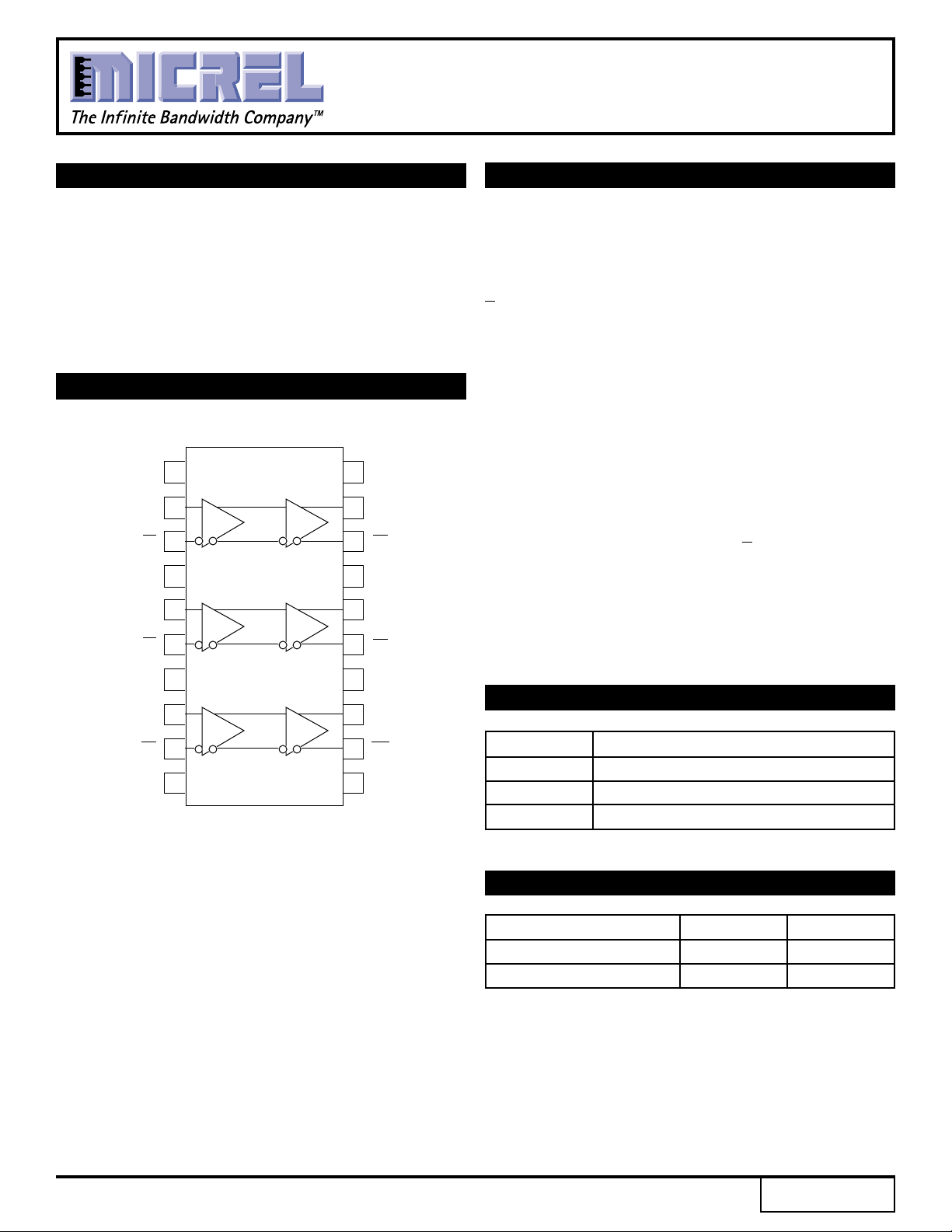
PIN CONFIGURATION/BLOCK DIAGRAM
ECL
20
V
CC
19
Q
0
Q
0
18
ECL
17
GND
16
Q
1
PECL_V
V
CC
1
2
D
3
D
B
4
5
D
1
PECL
PECL
DESCRIPTION
The SY100EL91L is a triple LVPECL-to-ECL or
LVPECL-to-LVECL translator.
A VBB output is provided for interfacing with single
ended PECL signals at the input. If a single ended input
is to be used, the VBB output should be connected to the
D input. The active signal would then drive the D input.
When used, the VBB output should be bypassed to ground
via a 0.01µF capacitor. The VBB output is designed to act
as the switching reference for the EL91L under single
ended input switching conditions. As a result this pin can
only source/sink up to 0.5mA of current.
To accomplish the level translation the EL91L requires
three power rails. The VCC supply should be connected
to the positive supply, and the VEE pin should be
connected to the negative power supply. The GND pins
as expected are connected to the system ground plane.
Both VEE and VCC should be bypassed to ground via
0.01µF capacitors.
Under open input conditions, the D input will be biased
at VCC/2 and the D input will be pulled to GND. This
condition will force the Q output to a LOW, ensuring
stability.
PECL_V
D
1
6
7
BB
8
D
D
2
9
V
EE
10 11
PECL
SOIC
TOP VIEW
15
Q
1
ECL
14
GND
PIN NAMES
Q
2
13
12
Q
2
Pin Function
Dn PECL Inputs
V
CC
Qn ECL Outputs
PECL_V
BB PECL Reference Voltage Output
FUNCTION TABLE
Function Vcc VEE
LVPECL-to-ECL 3.3V –5.0V
LVPECL-to-LVECL 3.3V –3.3V
Rev.: F Amendment: /2
1
Issue Date: November, 1999
Micrel
SY100EL91L
3.3V LVPECL INPUT DC ELECTRICAL CHARACTERISTICS
(1)
TA = –40°CTA = 0°CTA = +25°CTA = +85°C
Symbol Parameter Min. Typ. Max. Min. Typ. Max. Min. Typ. Max. Min. Typ. Max. Unit
VCC Power Supply Voltage 3.0 — 3.8 3.0 — 3.8 3.0 3.3 3.8 3.0 — 3.8 V
VIH Input HIGH Voltage
VIL Input LOW Voltage
(2)
2.135 — 2.420 2.135 — 2.420 2.135 2.350 2.420 2.135 — 2.420 V
(2)
1.490 — 1.825 1.490 — 1.825 1.490 — 1.825 1.490 — 1.825 V
IIH Input HIGH Current — — 150 — — 150 — — 150 — — 150 µA
IIL Input LOW Current Dn 0.5 — — 0.5 — — 0.5 — — 0.5 — — µA
Dn -600 — — -600 — — -600 — — -600 — —
VBB Output Reference
CC Power Supply Current — — 10 — — 10 — 6.0 10 — — 10 mA
I
NOTES:
1. Parametric values specified at: 3 volt Power Supply Range 100EL91L Series -3.0V to -3.8V.
2. These levels are for VCC = 3.3V. Level specifications will vary 1:1 with VCC.
ECL/LVECL OUTPUT DC ELECTRICAL CHARACTERISTICS
(2)
1.920 — 2.040 1.920 — 2.040 1.920 — 2.040 1.920 — 2.040 V
(1)
TA = –40°C TA = 0°CTA = +25°CTA = +85°C
Symbol Parameter Min. Typ. Max. Min. Typ. Max. Min. Typ. Max. Min. Typ. Max. Unit
VEE Power Supply ECL -4.2 — -5.5 -4.2 — -5.5 -4.2 — -5.5 -4.2 — -5.5 V
Voltage LVECL -3.0 — -3.8 -3.0 — -3.8 -3.0 — -3.8 -3.0 — -3.8
VOH Output HIGH Voltage -1085 — -880 -1025 — -880 -1025 -955 -880 -1025 — -880 mV
VOL Output LOW Voltage -1830 — -1555 -1810 — -1620 -1810 -1705 -1620 -1810 — -1620 mV
IEE Power Supply Current — — 28 — — 28 — 22 28 — — 30 mA
NOTE:
1. Parametric values specified at: 3 volt Power Supply Range 100EL91L Series -3.0V to -3.8V.
2
 Loading...