

MICREL SY10EL51, SY100EL51 Datasheet
DIFFERENTIAL
CLOCK D FLIP-FLOP
SY10EL51
SY100EL51
FEATURES
■ 475ps propagation delay
■ 2.8GHz toggle frequency
■ Internal 75KΩ input pull-down resistors
■ Available in 8-pin SOIC package
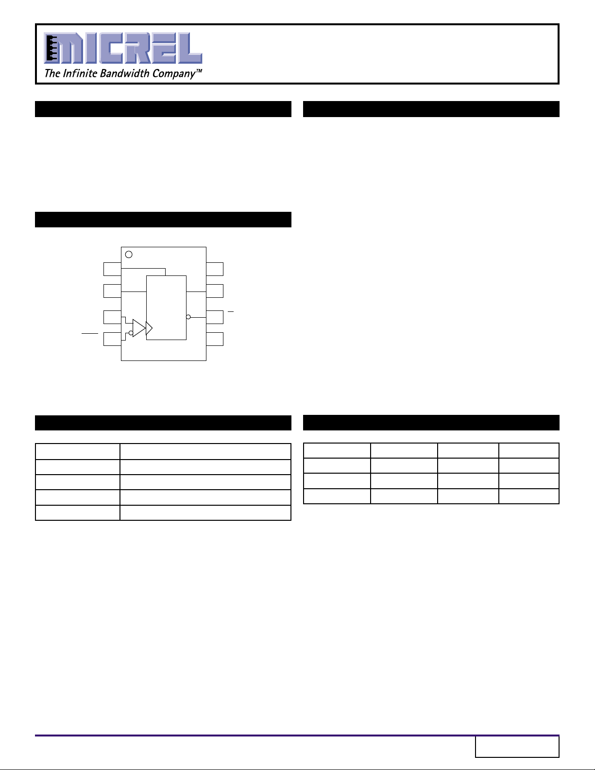
PIN CONFIGURATION/BLOCK DIAGRAM
1
RV
R
2
CLK
CLK
D
3
4
D
Flip-Flop
SOIC
TOP VIEW
8
CC
7
Q
6
Q
5
V
EE
DESCRIPTION
The SY10/100EL51 are differential clock D flip-flops
with reset. These devices are functionally similar to the
E151 devices, with higher performance capabilities. With
propagation delays and output transition times
significantly faster than the E151, the EL51 is ideally
suited for those applications which require the ultimate
in AC performance.
The reset input is an asynchronous, level triggered
signal. Data enters the master portion of the flip-flop
when the clock is LOW and is transferred to the slave,
and thus the outputs, upon a positive transition of the
clock. The differential clock inputs of the EL51 allow the
device to be used as a negative edge triggered flip-flop.
The differential input employs clamp circuitry to
maintain stability under open input (pulled down to VEE)
conditions.
PIN NAMES
Pin Function
R Reset Input
D Data Input
CLK Clock Input
Q Data Output
TRUTH TABLE
D R CLK Q
LLZL
HLZH
XHXL
NOTE:
1. Z = LOW-to-HIGH transition.
(1)
Rev.: E Amendment: /0
1
Issue Date: August, 1998
SY10EL51
Micrel
SY100EL51
DC ELECTRICAL CHARACTERISTICS
VEE = VEE (Min.) to VEE (Max.); VCC = GND
TA = –40°CTA = 0°CTA = +25°CTA = +85°C
Symbol Parameter Min. Typ. Max. Min. Typ. Max. Min. Typ. Max. Min. Typ. Max. Unit
EE Power Supply Current mA
I
10EL — 24 29 19 24 29 19 24 29 19 24 29
100EL — 24 29 19 24 29 19 24 29 24 30 36
EE Power Supply Voltage V
V
10EL –4.75 –5.2 –5.5 –4.75 –5.2 –5.5 –4.75 –5.2 –5.5 –4.75 –5.2 –5.5
100EL –4.20 –4.5 –5.5 –4.20 –4.5 –5.5 –4.20 –4.5 –5.5 –4.20 –4.5 –5.5
I
IH Input HIGH Current — — 150 — — 150 — — 150 — — 150 µA
AC ELECTRICAL CHARACTERISTICS
VEE = VEE (Min.) to VEE (Max.); VCC = GND
T
A = –40°CTA = 0°CTA = +25°CTA = +85°C
Symbol Parameter Min. Typ. Max. Min. Typ. Max. Min. Typ. Max. Min. Typ. Max. Unit
MAX Maximum Toggle 1.8 2.8 — 2.2 2.8 — 2.2 2.8 — 2.2 2.8 — GHz
f
Frequency
t
PLH Propagation Delay to ps
tPHL Output CLK 325 465 605 375 465 555 385 475 565 440 530 620
R 305 455 605 355 455 555 355 465 565 410 510 620
tS Set-up Time 150 0 — 150 0 — 150 0 — 150 0 — ps
tH Hold Time 250 100 — 250 100 — 250 100 — 250 100 — ps
tRR Reset Recovery 400 200 — 400 200 — 400 200 — 400 200 — ps
PW Minimum Pulse Width 400 — — 400 — — 400 — — 400 — — ps
t
CLK, Reset
PP Minimum Input 150 — — 150 — — 150 — — 150 — — mV
V
VCMR Common Mode (2) — –0.4 (2) — –0.4 (2) — –0.4 (2) — –0.4 V
tr Output Rise/Fall Times Q 100 225 350 100 225 350 100 225 350 100 225 350 ps
tf (20% to 80%)
NOTES:
1. Minimum input swing for which AC parameters are guaranteed.
2. The CMR range is referenced to the most positive side of the differential input signal. Normal operation is obtained if the HIGH level falls within the specified
range and the peak-to-peak voltage lies between VPP min. and 1V. The lower end of the CMR range is dependent on VEE and is equal to VEE + 3.0V.
Swing
Range
(1)
(2)
PRODUCT ORDERING CODE
Ordering Package Operating
Code Type Range
SY10EL51ZC Z8-1 Commercial
SY10EL51ZCTR Z8-1 Commercial
SY100EL51ZC Z8-1 Commercial
SY100EL51ZCTR Z8-1 Commercial
2
 Loading...