

MICREL SY100EL14V Datasheet
5V/3.3V 1:5 CLOCK
DISTRIBUTION
FEATURES DESCRIPTION
ClockWorks™
SY100EL14V
■ 3.3V and 5V power supply options
■ Typical 30ps output-to-output skew
■ Max. 50ps output-to-output skew
■ Synchronous enable/disable
■ Multiplexed clock input
■ 75KΩ internal input pull-down resistors
■ Available in 20-pin SOIC package
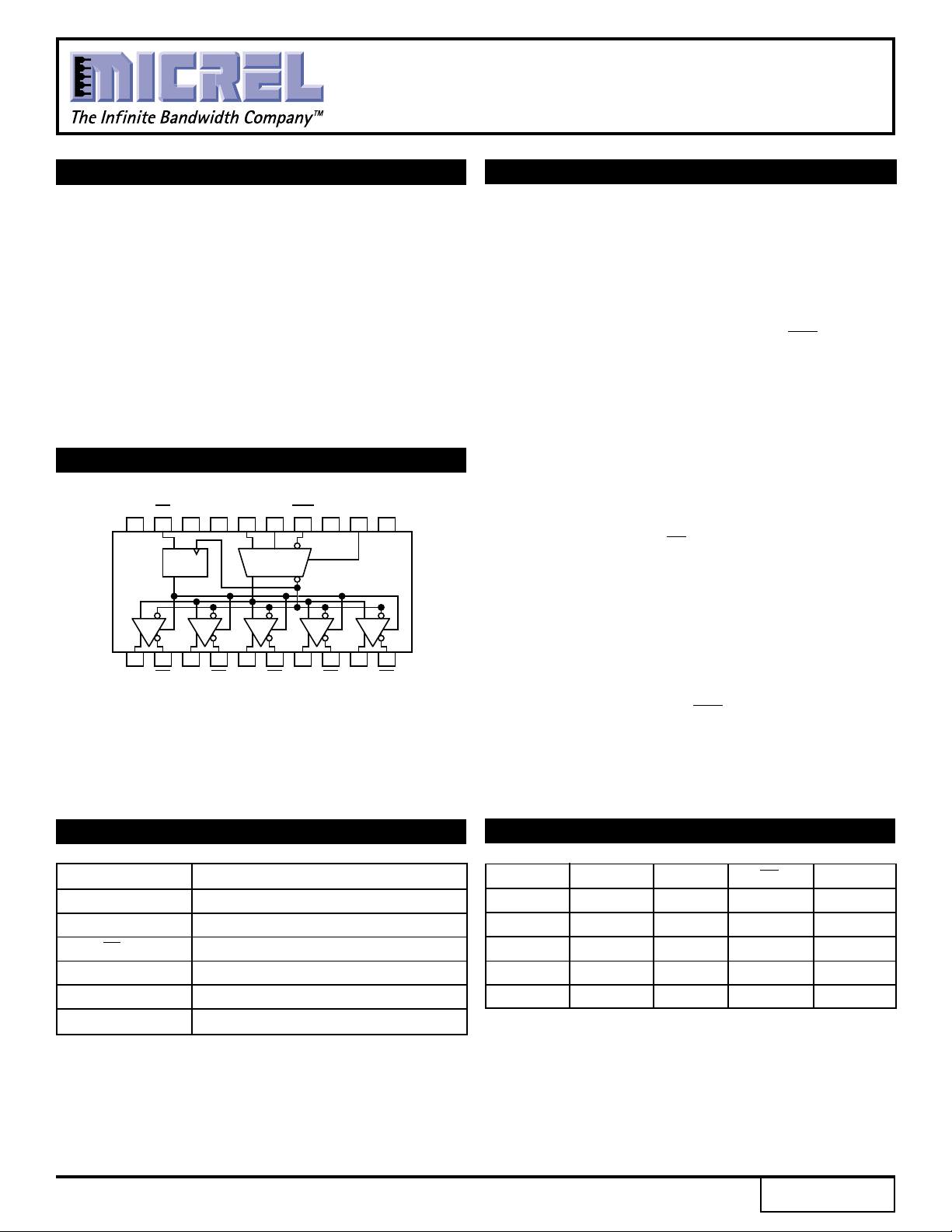
PIN CONFIGURATION/BLOCK DIAGRAM
V
CC
EN VCC NC SCLK CLK CLK VBBSEL V
20
Q
1
21931841751661571481391210
Q0 Q0 Q1 Q1 Q2 Q2 Q3 Q3 Q4 Q4
10D
SOIC
TOP VIEW
EE
11
The SY100EL14V is a low skew 1:5 clock distribution
chip designed explicitly for low skew clock distribution
applications. The device can be driven by either a
differential or single-ended ECL or, if positive power
supplies are used, PECL input signal. The EL14V is
suitable for operation in systems operating from 3.3V to
5.0V supplies. If a single-ended input is to be used the
VBB output should be connected to the CLK input and
bypassed to ground via a 0.01µF capacitor. The VBB
output is designed to act as the switching reference for
the input of the EL14V under single-ended input
conditions, as a result this pin can only source/sink up to
0.5mA of current.
The EL14V features a multiplexed clock input to allow
for the distribution of a lower speed scan or test clock
along with the high speed system clock. When LOW (or
left open and pulled LOW by the input pull-down resistor)
the SEL pin will select the differential clock input.
The common enable (EN) is synchronous so that the
outputs will only be enabled/disabled when they are
already in the LOW state. This avoids any chance of
generating a runt clock pulse when the device is enabled/
disabled as can happen with an asynchronous control.
The internal flip flop is clocked on the falling edge of the
input clock, therefore all associated specification limits
are referenced to the negative edge of the clock input.
When both differential inputs are left open, CLK input
will pull down to VEE and CLK input will bias around
VCC/2.
Pin Function
CLK Differential Clock Inputs
SCLK Scan Clock Input
EN Synchronous Enable
SEL Clock Select Input
VBB Reference Output
Q0-4 Differential Clock Outputs
TRUTH TABLEPIN NAMES
CLK SCLK SEL EN Q
L XLLL
HXLLH
XLHLL
XHHLH
XXXHL*
* On next negative transition of CLK or SCLK
1
Rev.: A Amendment: /0
Issue Date: October 1999

Micrel
ClockWorks™
SY100EL14V
ABSOLUTE MAXIMUM RATINGS
(1)
Symbol Rating Value Unit
VEE Power Supply (VCC = 0V) -8.0 to 0 VDC
(3)
VI
OUT Output Current
I
Input Voltage (VCC = 0V) 0 to -6.0 VDC
- Continuous 50 mA
- Surge 100
TA Operating Temperature Range -40 to +85 °C
EE Operating Range
V
NOTES:
1. Absolute maximum rating, beyond which, device life may be impaired, unless otherwise specified on an individual data sheet.
2. Parametric values specified at: 100EL14V Series: -3.0V to -5.5V.
3. In PECL mode operation, VI(Max) = VCC.
(1),(2)
-5.7 to -3.0 V
DC ELECTRICAL CHARACTERISTICS
VEE = VEE (Min) to VEE (Max); VCC = GND
Symbol Parameter Min. Typ. Max. Min. Typ. Max. Min. Typ. Max. Min. Typ. Max. Unit
VOH Output HIGH Voltage
VOL Output LOW Voltage
VOHA Output HIGH Voltage
VOLA Output LOW Voltage
VIH Input HIGH Voltage
VIL Input LOW Voltage
IL Input LOW Current
I
IIH Input High Current — — 150 — — 150 — — 150 — — 150 µA
IEE Power Supply Current — 32 40 — 32 40 — 32 40 — 34 42 mA
BB Output Reference
V
Voltage
(2)
-1085 -1005 -880 -1025 -955 -880 -1025 -955 -880 -1025 -955 -880
(2)
-1830 -1695 -1555 -1810 -1705 -1620 -1810 -1705 -1620 -1810 -1705 -1620
(2)
-1095 — — -1035 — — -1035 — — -1035 — —
(2)
-1165 — -880 -1165 — -880 -1165 — -880 -1165 — -880
-1810 — -1475 -1810 — -1475 -1810 — -1475 -1810 — -1475
(3)
CLK -300 — — -300 — — -300 — — -300 — —
-1.38 — -1.26 -1.38 — -1.26 -1.38 — -1.26 -1.38 — -1.26
(1)
TA = –40°CTA = 0°CTA = +25°CTA = +85°C
— — -1555 — — -1610 — — -1610 — — -1610
0.5 — — 0.5 — — 0.5 — — 0.5 — — µA
mV
mV
mV
mV
mV
mV
V
NOTES:
1. This table replaces the three traditionally seen in ECL 100K data books. The same DC parameter values at VEE = -4.5V now apply across the full VEE
range of -3.0V to -5.5V. Outputs are terminated through a 50Ω resistor to -2.0V except where otherwise specified on the individual data sheets.
2. VIN = VIH(Max) or VIL(Min).
3. VIN = VIL(Max).
2
 Loading...