

MICREL SY10E457, SY100E457 Datasheet
TRIPLE DIFFERENTIAL
2:1 MULTIPLEXER
SY10E457
SY100E457
FEATURES
■ Differential D and Q
■ Extended 100E V
EE range of –4.2V to –5.5V
■ VBB output for single-ended use
■ 700ps max. propagation delay
■ High frequency outputs
■ Separate and common select
■ Internal 75KΩ input pulldown resistors
■ Available in 28-pin PLCC package
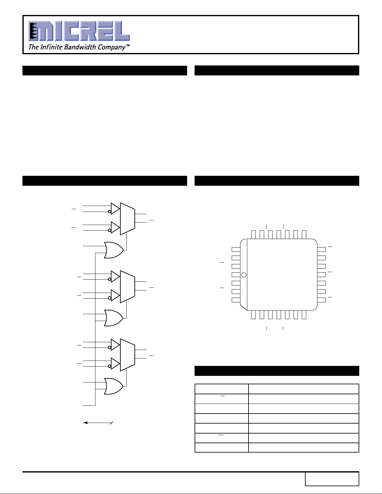
BLOCK DIAGRAM
D
D
D
D
SEL
D
D
D
D
SEL
0a
0a
0b
0b
0
1a
1a
1b
1b
1
H
2:1
MUX
L
H
2:1
MUX
L
DESCRIPTION
The SY10/100E457 are 3-bit differential 2:1
multiplexers. The fully differential data path makes the
devices ideal for multiplexing low skew clock or other
skew sensitive signals. Multiple VBB pins are provided to
ease AC coupling input signals.
The higher frequency outputs provide the device with
a >1.0GHz bandwidth to meet the needs of the most
demanding system clock.
Both separate selects and a common select are
provided to make the device well suited for both data
path and random logic applications.
PIN CONFIGURATION
Q
0
Q
0
SEL1
D1a
D1a
VEE
Q
1
Q
1
VBB
D1b
D1b
SEL2
D2a
25
24 23 22 21 20 19
26
27
28
1
2
3
4
TOP VIEW
567891011
D2a
VBB
PLCC
J28-1
2b
D
COMSEL
D2b
18
Q2
17
Q2
16
VCC
15
Q1
14
Q1
13
Q0
12
Q0
D
D
D
D
SEL
COMSEL
V
BB
D0a
SEL0
2a
2a
2b
2b
2
H
2:1
MUX
L
Q
2
Q
2
PIN NAMES
D0b
VBB
D0b
VCCO
D0a
Pin Function
Dn[0:2], Dn[0:2] Differential Data Inputs
SEL Individual Select Input
COMSEL Common Select Input
VBB VBB Reference Output
Q[0:2], Q[0:2] Differential Data Outputs
CCO VCC to Output
V
Rev.: C Amendment: /1
1
Issue Date: February, 1998
SY10E457
Micrel
SY100E457
DC ELECTRICAL CHARACTERISTICS
VEE = VEE (Min.) to VEE (Max.); VCC = VCCO = GND
TA = 0°CTA = +25°CTA = +85°C
Symbol Parameter Min. Typ. Max. Min. Typ. Max. Min. Typ. Max. Unit Condition
V
BB Output Reference Voltage V—
10E –1.38 — –1.27 –1.35 — –1.25 –1.31 — –1.19
100E –1.38 — –1.26 –1.38 — –1.26 –1.38 — –1.26
IIH Input HIGH Current — — 150 — — 150 — — 150 µA—
EE Power Supply Current mA —
I
10E — 92 110 — 92 110 — 92 110
100E — 92 110 — 92 110 — 106 127
VPP (DC) Input Sensitivity 50 — — 50 — — 50 — — mV 1
CMR Common Mode Range –1.5 — 0 –1.5 — 0 –1.5 — 0 V 2
V
NOTES:
1. Differential input voltage required to obtain a full ECL swing on the outputs.
2. VCMR is referenced to the most positive side of the differential input signal. Normal operation is obtained when the input signals are within the VCMR range
and the input swing is greater than VPP (min.) and <1V.
AC ELECTRICAL CHARACTERISTICS
VEE = VEE (Min.) to VEE (Max.); VCC = VCCO = GND
TA = 0°CTA = +25°CTA = +85°C
Symbol Parameter Min. Typ. Max. Min. Typ. Max. Min. Typ. Max. Unit Condition
PLH Propagation Delay to Output ps —
t
tPHL D (Diff) 375 475 650 375 475 650 375 475 650
D 325 475 700 325 475 700 325 475 700
SEL 350 500 725 350 500 725 350 500 725
COMSEL 375 525 750 375 525 750 375 525 750
tskew Within-Device Skew — 40 — — 40 — — 40 — ps 1
tskew Duty Cycle Skew tPLH–tPHL — ±10 — — ±10 — — ±10 — ps 2
VPP (AC) Minimum Input Swing 150 — — 150 — — 150 — — mV 3
r Rise/Fall Time 150 275 450 150 275 450 150 275 450 ps —
t
tf 20–80%
NOTES:
1. Within-device skew is defined as identical transitions on similar paths through a device.
2. Duty cycle skew guarantee holds only for differential operation when the delays are measured from the cross point of the inputs to the cross point of the
outputs.
3. Minimum input swing for which AC parameters are guaranteed.
PRODUCT ORDERING CODE
Ordering Package Operating
Code Type Range
SY10E457JC J28-1 Commercial
SY10E457JCTR J28-1 Commercial
SY100E457JC J28-1 Commercial
SY100E457JCTR J28-1 Commercial
2
 Loading...