

MICREL SY10E452, SY100E452 Datasheet
Pin Function
D [0:4], /D [0:4] Differential Data Inputs
MR Master Reset Input
CLK, /CLK Differential Clock Input
VBB VBB Reference Output
Q [0:4], Q [0:4] Differential Data Outputs
V
CCO VCC to Output
DESCRIPTION
FEATURES
■ Differential D, CLK and Q
■ Extended 100E VEE range of –4.2V to –5.5V
■ VBB output for single-ended use
■ 1100MHz min. toggle frequency
■ Asynchronous Master Reset
■ Fully compatible with Motorola MC10E/100E452
■ Available in 28-pin PLCC package
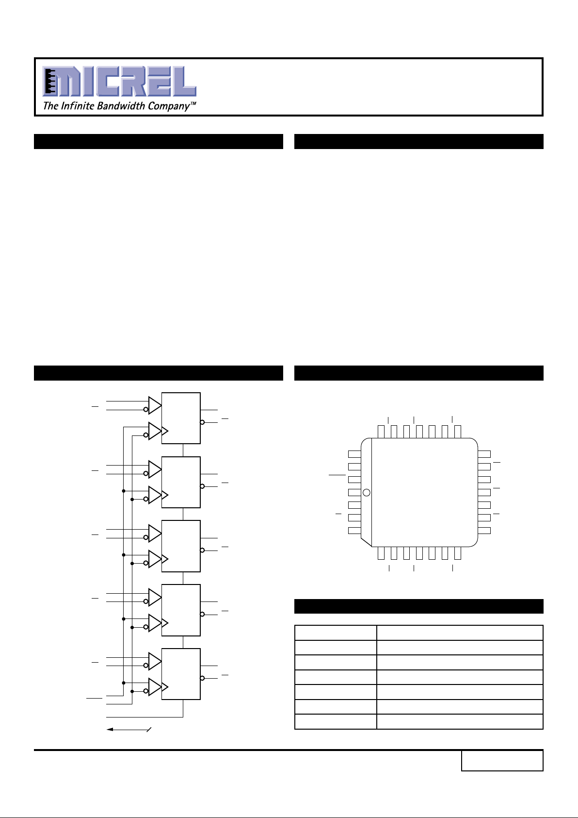
The SY10/100E452 are 5-bit differential registers with
differential data (inputs and outputs) and clock. The
registers are triggered by a positive transition of the
positive clock (CLK) input. A high on the Master Reset
(MR) asynchronously resets all registers so that the Q
outputs go LOW.
The differential input structures are clamped so that
the inputs of unused registers can be left open without
upsetting the bias network of the devices. The clamping
action will assert the /D and the /CLK sides of the inputs.
Because of the edge-triggered flip-flop nature of the
devices, simultaneously opening both the clock and data
inputs will result in an output which reaches an
unidentified but valid state.
The fully differential design of the devices makes them
ideal for very high frequency applications where a
registered data path is necessary.
5-BIT DIFFERENTIAL
REGISTER
SY10E452
SY100E452
Rev.: D Amendment: /0
Issue Date: May, 1999
BLOCK DIAGRAM
D
0
D
0
Q
0
Q
0
V
BB
CLK
CLK
D
Q
R
MR
D
1
D
1
Q
1
Q
1
D
Q
R
D
2
D
2
Q
2
Q
2
D
Q
R
D
3
D
3
Q
3
Q
3
D
Q
R
D
4
D
4
Q
4
Q
4
D
Q
R
PIN CONFIGURATION
PIN NAMES
18
17
16
15
14
13
12
567891011
26
27
28
1
2
3
4
TOP VIEW
PLCC
J28-1
25
24 23 22 21 20 19
MR
CLK
V
EE
V
BB
D
2
CLK
D
2
D
1
D
0
V
CCO
Q
0
D1D
0
Q
0
Q
3
V
CC
Q
2
Q
1
Q
3
Q
2
Q
1
D
4
V
CCO
Q
4
D
3
D
3
D
4
Q
4
1
2
SY10E452
SY100E452
Micrel
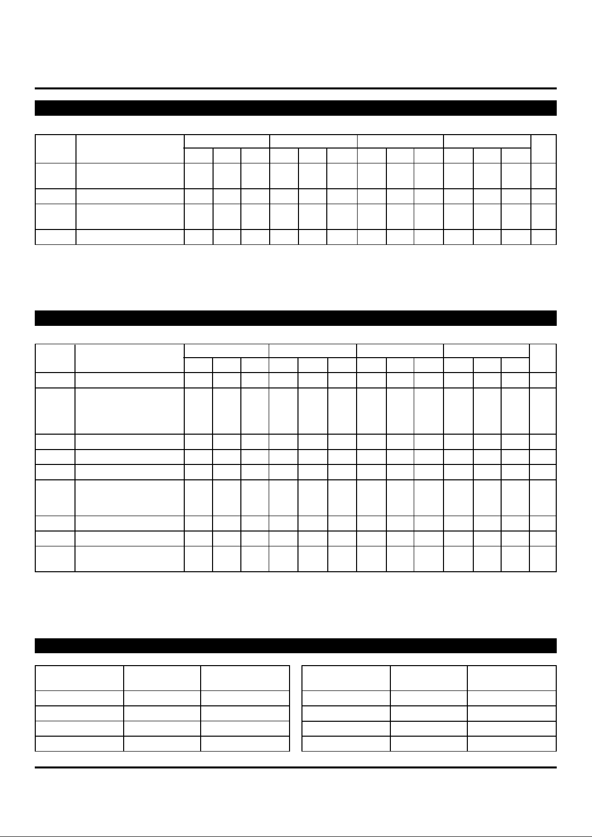
DC ELECTRICAL CHARACTERISTICS
VEE = VEE (Min.) to VEE (Max.); VCC = VCCO = GND
TA = -40°CTA = 0°CTA = +25°CTA = +85°C
Symbol Parameter Min. Typ. Max. Min. Typ. Max. Min. Typ. Max. Min. Typ. Max. Unit
V
BB Output Reference 10E -1.43 — -1.30 -1.38 — -1.27 -1.35 — -1.25 -1.31 — -1.19 V
Voltage 100E -1.38 — -1.26 -1.38 — -1.26 -1.38 — -1.26 -1.38 — -1.26
IIH Input HIGH Current — — 150 — — 150 — — 150 — — 150 µA
I
EE Power Supply 10E — 74 89 — 74 89 — 74 89 — 74 89 mA
Current 100E — 74 89 — 74 89 — 74 89 — 85 102
V
CMR Common Mode Range
(1)
-2.0 — -0.4 -2.0 — -0.4 -2.0 — -0.4 -2.0 — -0.4 V
NOTE:
1. VCMR is referenced to the most positive side of the differential input signal. Normal operation is obtained when the input signals are within the VCMR range
and the input swing is greater than VPP (min.) and <1V.
AC ELECTRICAL CHARACTERISTICS
VEE = VEE (Min.) to VEE (Max.); VCC = VCCO = GND
TA = -40°CTA = 0°CTA = +25°CTA = +85°C
Symbol Parameter Min. Typ. Max. Min. Typ. Max. Min. Typ. Max. Min. Typ. Max. Unit
fMAX Max. Toggle Frequency 1000 1400 — 1100 1400 — 1100 1400 — 1100 1400 — MHz
t
PLH Propagation Delay to ps
tPHL Output CLK (Diff) 425 600 850 475 600 800 475 600 800 475 600 800
CLK (SE) 375 600 900 425 600 850 425 600 850 425 600 850
MR 375 625 900 425 625 850 425 625 850 425 625 850
tS Set-up Time, D 175 –50 — 150 –50 — 150 –50 — 150 –50 — ps
tH Hold Time, D 225 50 — 200 50 — 200 50 — 200 50 — ps
tRR Reset Recovery Time 750 450 — 700 450 — 700 450 — 700 450 — ps
t
PW Minimum Pulse Width ps
CLK 400 — — 400 — — 400 — — 400 — —
MR 400 — — 400 — — 400 — — 400 — —
tskew Within-Device Skew
(1)
—50——50——50——50—ps
VPP (AC) Minimum Input Swing
(2)
150 — — 150 — — 150 — — 150 — — mV
t
r Rise/Fall Time 250 475 725 275 475 675 275 475 675 275 475 675 ps
tf 20–80%
NOTES:
1. Within-device skew is defined as identical transitions on similar paths through a device.
2. Minimum input swing for which AC parameters are guaranteed.
Ordering Package Operating
Code Type Range
SY10E452JI J28-1 Industrial
SY10E452JITR J28-1 Industrial
SY100E452JI J28-1 Industrial
SY100E452JITR J28-1 Industrial
PRODUCT ORDERING CODE
Ordering Package Operating
Code Type Range
SY10E452JC J28-1 Commercial
SY10E452JCTR J28-1 Commercial
SY100E452JC J28-1 Commercial
SY100E452JCTR J28-1 Commercial
 Loading...