

MICREL SY10E337, SY100E337 Datasheet
3-BIT SCANNABLE
REGISTERED BUS
TRANSCEIVER
SY10E337
SY100E337
FEATURES
■ 1500ps max. clock to bus (data transmit)
■ 1000ps max. clock to Q (data receive)
■ Extended 100E VEE range of –4.2V to –5.5V
■ 25Ω cutoff bus outputs
■ 50Ω receiver outputs
■ Scannable implementation of E336
■ Synchronous and asynchronous bus enables
■ Non-inverting data path
■ Bus outputs feature internal edge slow-down
capacitors
■ Additional package ground pins
■ Fully compatible with industry standard 10KH,
100K ECL levels
■ Internal 75KΩ input pulldown resistors
■ Fully compatible with Motorola MC10E/100E337
■ Available in 28-pin PLCC package
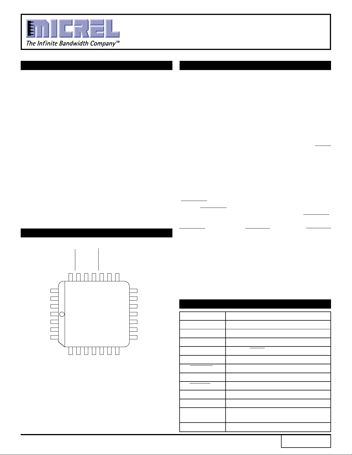
PIN CONFIGURATION
0
CCO
Q
V
ABUSDIS
Q2
GND
BUS2
18
GND
17
BUS0
16
VCC
15
Q
1
14
VCCO
13
BUS1
12
GND
SCAN
S-IN
TEN
VEE
REN
CLK
A1
SBUSEN
SYNCEN
B0
A0
25 24 23 22 21 20 19
26
27
28
1
2
3
4
TOP VIEW
PLCC
J28-1
5 6 7 8 9 10 11
B2
B1
A2
VCCO
DESCRIPTION
The SY10/100E337 are 3-bit registered bus transceivers
with scan designed for use in new, high- performance ECL
systems. The bus outputs (BUS0–BUS2) are designed to
drive a 25Ω bus; the receive outputs (Q0–Q2) are designed
for 50Ω. The bus outputs feature a normal logic HIGH level
(VOH) and a cutoff LOW level of –2.0V and the output
emitter-follower is “off”, presenting a high impedance to the
bus. The bus outputs also feature edge slow-down
capacitors.
Both drive and receive sides feature the same logic,
including a loopback path to hold data. The LOAD/HOLD
function is controlled by Transmit Enable (TEN) and Receive
Enable (REN) on the transmit and receive sides,
respectively, with a HIGH selecting LOAD. The
implementation of the E337 Receive Enable differs from
that of the E336.
A synchronous bus enable (SBUSEN) is provided for
normal, non-scan operation. The asynchronous bus disable
(ABUSDIS) disables the bus for scan mode.
The SYNCEN input allows either synchronous or
asynchronous re-enabling after disabling with ABUSDIS.
An alternative use is asynchronous-only operation with
ABUSDIS, in which case SYNCEN is tied LOW. SYNCEN
is implemented as an overriding SET control to the enable
flip-flop.
Scan mode is selected by a logic HIGH at the SCAN
input. Scan input data is shifted in through S-IN, and output
data appears at the Q2 output.
All registers are clocked on the rising edge of CLK.
Additional lead-frame grounding is provided through the
ground pins (GND) which should be connected to 0V. The
GND pins are not electrically connected to the chip.
PIN NAMES
Pin Function
A0–A2 Data Inputs A
B0–B2 Data Inputs B
S-IN Serial (Scan) Data Input
TEN, REN LOAD/HOLD Controls
SCAN Scan Control
ABUSDIS Asynchronous Bus Disable
SBUSEN Synchronous Bus Enable
SYNCEN Synchronous Enable Control
CLK Clock
BUS0–BUS2 25Ω Cutoff BUS Outputs
Q
0–Q2 Receive Data Outputs (Q2 serves as
SCAN_OUT in scan mode)
VCCO VCC to Output
Rev.: C Amendment: /2
1
Issue Date: February, 1998

Micrel
BLOCK DIAGRAM
SY10E337
SY100E337
BUS
2
Q
D
Q
A
2
B
2
D
Q
2
SCAN-OUT
BUS
1
A0
B0
S-IN
TEN
REN
SCAN
ABUSDIS
SBUSEN
SYNCEN
CLK
D
D
D
SET
Q
Q
Q
1
A
B
1
D
Q
D
Q
Q
1
BUS
Q
0
0
2
 Loading...