

MICREL SY10E256, SY100E256 Datasheet
3-BIT 4:1
MUX-LATCH
SY10E256
SY100E256
FEATURES
■ 950ps max. data to output
■ Extended 100E V
EE range of –4.2V to –5.5V
■ 850ps max. latch enable to output
■ Separate select controls
■ Differential outputs
■ Fully compatible with industry standard 10KH,
100K ECL levels
■ Internal 75KΩ input pulldown resistors
■ Fully compatible with Motorola MC10E/100E256
■ Available in 28-pin PLCC package
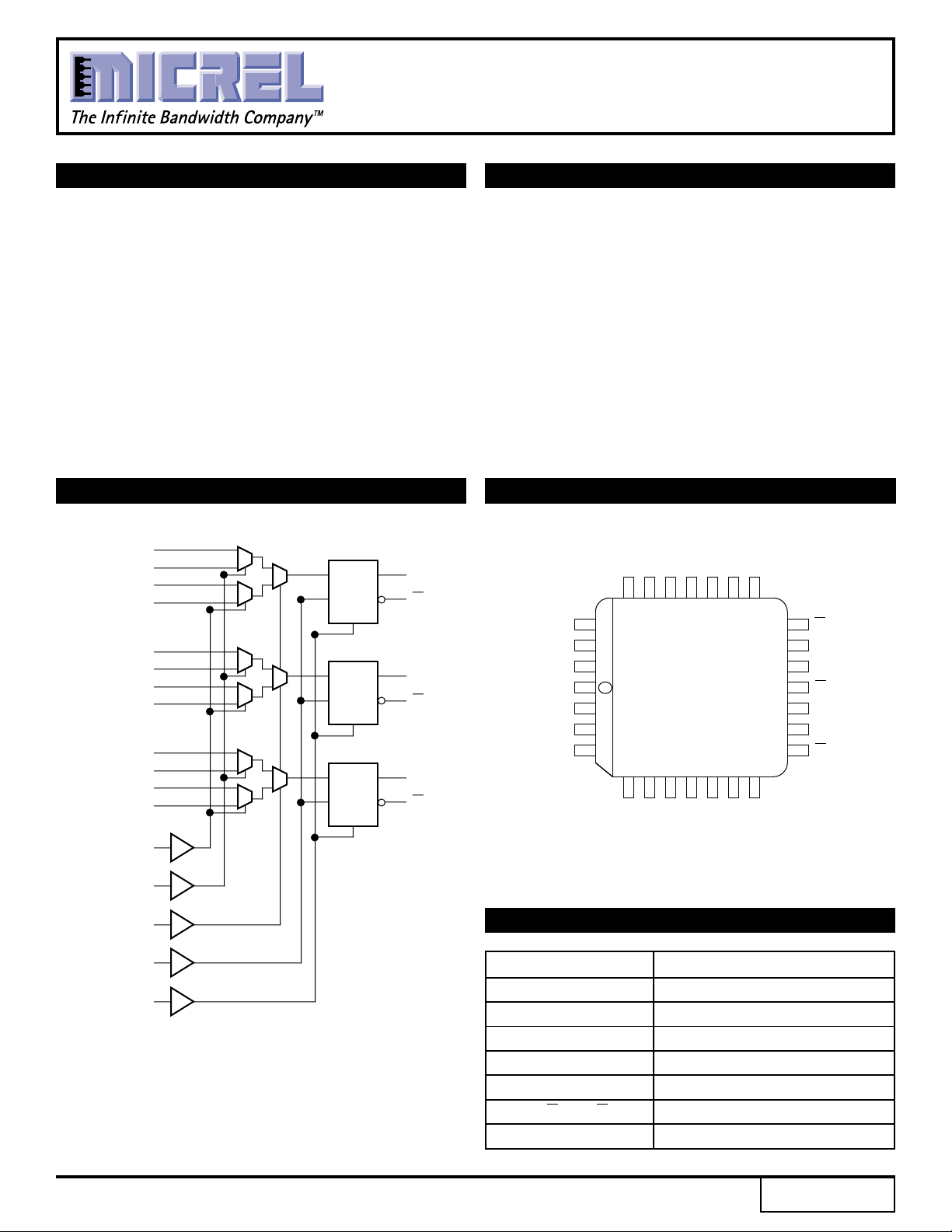
BLOCK DIAGRAM
D
0a
D
SEL
0b
D
0c
D
0d
D
1a
D
1b
D
1c
D
1d
D
2a
D
2b
D
2c
D
2d
1A
D
E
N
R
D
E
N
R
D
E
N
R
Q
Q
Q
Q
Q
Q
DESCRIPTION
The SY10/100E256 offer three 4:1 multiplexers followed
by latches with differential outputs designed for use in new,
high-performance ECL systems. Separate Select controls
are provided for the leading 2:1 mux pairs (see block
diagram).
When the Latch Enable (LEN) is at a logic LOW, the latch
is transparent and output data is controlled by the multiplexer
select controls. A logic HIGH on LEN latches the outputs.
The Master Reset (MR) overrides all other controls to set
the Q outputs LOW.
PIN CONFIGURATION
2d
1b
0
0
1A
SEL
SEL
1B
SEL
1
1
V
EE
LEN
2
MR
D
1c
2
2
D
25
24 23 22 21 20 19
26
27
28
1
2
3
4
5 6 7 8 9 10 11
1d
D
2c
1a
D
D
D
TOP VIEW
PLCC
J28-1
0c
0a
0b
D
D
D
2b
CCO
2a
V
D
D
18
Q
2
17
Q
2
16
V
CC
15
Q
1
14
Q
1
13
V
CCO
12
Q
0
0
0d
Q
D
CCO
V
SEL
SEL
LEN
1B
MR
2
PIN NAMES
Pin Function
D0x–D2x Parallel Data Inputs
SEL1A, SEL1B First-stage Select Inputs
SEL2 Second-stage Select Input
LEN Latch Enable
MR Master Reset
Q0, Q0–Q2, Q2 Data Outputs
CCO VCC to Output
V
Rev.: C Amendment: /1
1
Issue Date: February, 1998

Micrel
SY100E256
TRUTH TABLE
Pin State Operation
SEL2 H Output c/d Data
SEL1A H Input d Data
SEL
1B H Input b Data
DC ELECTRICAL CHARACTERISTICS
VEE = VEE (Min.) to VEE (Max.); VCC = VCCO = GND
TA = 0°CTA = +25°CTA = +85°C
Symbol Parameter Min. Typ. Max. Min. Typ. Max. Min. Typ. Max. Unit Condition
IIH Input HIGH Current ——150 ——150 ——150 µA —
EE Power Supply Current mA —
I
10E — 69 83 — 69 83 — 69 83
100E — 69 83 — 69 83 — 79 96
AC ELECTRICAL CHARACTERISTICS
SY10E256
VEE = VEE (Min.) to VEE (Max.); VCC = VCCO = GND
TA = 0°CTA = +25°CTA = +85°C
Symbol Parameter Min. Typ. Max. Min. Typ. Max. Min. Typ. Max. Unit Condition
PLH Propagation Delay to Output ps —
t
tPHL D 400 600 900 400 600 900 400 600 900
SEL1 550 775 1050 550 775 1050 550 775 1050
SEL2 450 650 900 450 650 900 450 650 900
LEN 350 500 800 350 500 800 350 500 800
MR 350 600 825 350 600 825 350 600 825
S Set-up Time ps —
t
D 400 275 — 400 275 — 400 275 —
SEL1 600 300 — 600 300 — 600 300 —
SEL2 500 250 — 500 250 — 500 250 —
H Hold Time ps —
t
D 300 –275 — 300 –275 — 300 –275 —
SEL1 100 –300 — 100 –300 — 100 –300 —
SEL2 200 –250 — 200 –250 — 100 –250 —
tRR Reset Recovery Time 700 600 — 700 600 — 700 600 — ps —
tPW Minimum Pulse Width, MR 400 ——400 ——400 ——ps —
tskew Within-Device Skew — 50 ——50 ——50 — ps 1
r Rise/Fall Time 275 475 700 275 475 700 275 475 700 ps —
t
tf 20% to 80%
NOTE:
1. Within-device skew is defined as identical transitions on similar paths
through a device.
PRODUCT ORDERING CODE
Ordering Package Operating
Code Type Range
SY10E256JC J28-1 Commercial
SY10E256JCTR J28-1 Commercial
SY100E256JC J28-1 Commercial
SY100E256JCTR J28-1 Commercial
2
 Loading...