

MICREL SY10E241, SY100E241 Datasheet
■ 1000ps max. CLK to output
■ Extended 100E V
EE range of –4.2V to –5.5V
■ SHIFT overrides HOLD, /LOAD control
■ Asynchronous Master Reset
■ Pin-compatible with E141
■ Fully compatible with industry standard 10KH,
100K ECL levels
■ Internal 75KΩ input pulldown resistors
■ Fully compatible with Motorola MC10E/100E241
■ Available in 28-pin PLCC package
FEATURES
8-BIT SCANNABLE
REGISTER
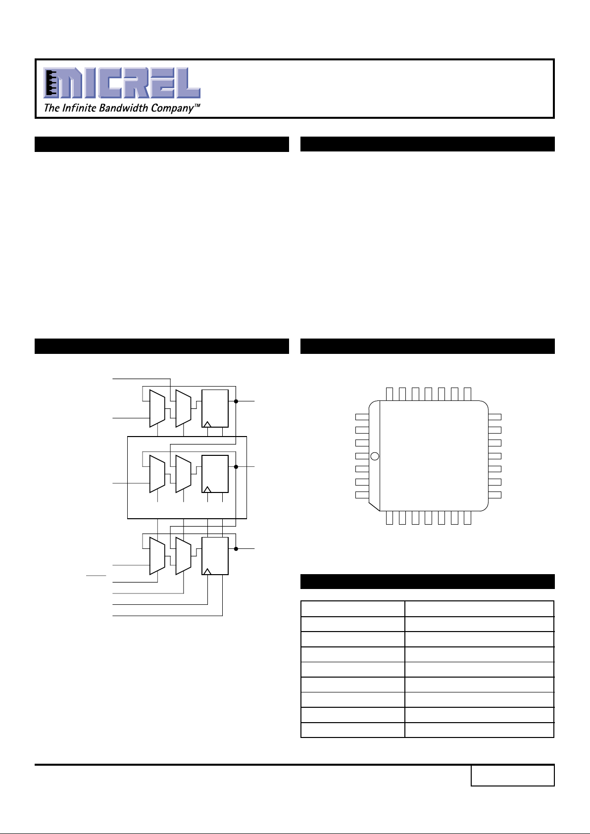
The SY10/100E241 are 8-bit shiftable registers designed
for use in new, high-performance ECL systems. Unlike the
E141, the E241 features internal data feedback organized
such that the SHIFT control overrides the HOLD, /LOAD
control. Thus, the normal operations of HOLD and LOAD
can be toggled with a single control line without the need for
external gating. This configuration also enables switching
to scan mode with the single SHIFT control line.
The eight inputs D
0–D7 accept parallel input data, while
S-IN accepts serial input data when in shift mode. Data is
accepted a set-up time before the rising edge of CLK.
Shifting is also accomplished on the rising clock edge. A
HIGH on the Master Reset pin (MR) asychronously resets
all the registers to zero.
DESCRIPTION
SY10E241
SY100E241
Rev.: C Amendment: /1
Issue Date: February, 1998
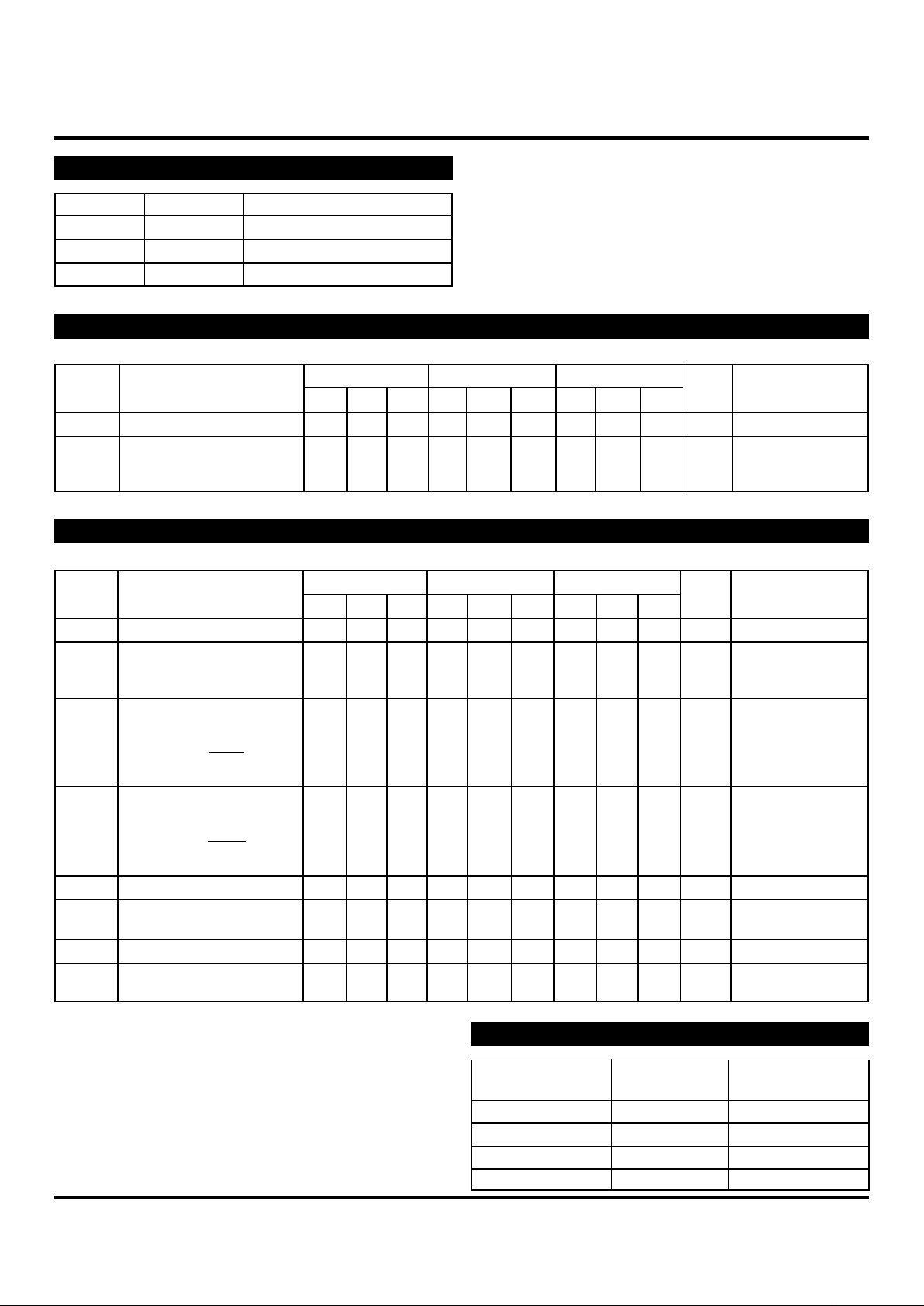
PIN CONFIGURATION
Pin Function
D0–D7 Parallel Data Inputs
S-IN Serial Data Input
SEL0 SHIFT Control
SEL1 HOLD, /LOAD Control
CLK Clock
MR Master Reset
Q0–Q7 Data Outputs
V
CCO VCC to Output
PIN NAMES
BLOCK DIAGRAM
TOP VIEW
PLCC
J28-1
26
27
28
1
2
3
4
18
17
16
15
14
13
12
25 24 23 22 21 20 19
567891011
D3
D2
Q2
VCCO
D4
Q0
Q1
VEE
D1
SEL1
CLK
D0
MR
S-IN
VCC
Q3
NC
VCCO
Q4
Q5
Q6
NC
SEL
0
VCCO
D7
D6
D5
Q7
R
D
S-IN
Q
R
D
Q
R
D
Q
BITS 1-6
SEL0 (SHIFT)
CLK
MR
SEL1 (HOLD/LOAD)
D0
D7
D1 – D6
Q0
Q7
Q1 – Q6
1
2
SY10E241
SY100E241
Micrel
TRUTH TABLE
SEL0 SEL1 Function
L L Load
L H Hold
H X Shift (D
n to Dn+1)
VEE = VEE (Min.) to VEE (Max.); VCC = VCCO = GND
TA = 0°CTA = +25°CTA = +85°C
Symbol Parameter Min. Typ. Max. Min. Typ. Max. Min. Typ. Max. Unit Condition
fSHIFT Max. Shift Frequency 700 900 — 700 900 — 700 900 — MHz —
t
PLH Propagation Delay to Output ps —
tPHL CLK 625 750 975 625 750 975 625 750 975
MR 600 725 975 600 725 975 600 725 975
t
S Set-up Time ps —
D17525— 175 25 — 175 25 —
SEL0 (SHIFT)350 200 — 350 200 — 350 200 —
SEL1 (HOLD/LOAD) 400 250 — 400 250 — 400 250 —
S-IN 125 –100 — 125 –100 — 125 –100 —
t
H Hold Time ps —
D200–25 — 200 –25 — 200 –25 —
SEL0 (SHIFT) 100 –200 — 100 –200 — 100 –200 —
SEL1 (HOLD/LOAD) 50 –250 — 50 –250 — 50 –250 —
S-IN 300 100 — 300 100 — 300 100 —
tRR Reset Recovery Time 900 600 — 900 600 — 900 600 — ps —
t
PW Minimum Pulse Width 400 ——400 ——400 ——ps —
CLK, MR
tskew Within-Device Skew — 60 ——60 ——60 — ps 1
t
r Rise/Fall Time 300 525 800 300 525 800 300 525 800 ps —
tf 20% to 80%
AC ELECTRICAL CHARACTERISTICS
DC ELECTRICAL CHARACTERISTICS
VEE = VEE (Min.) to VEE (Max.); VCC = VCCO = GND
TA = 0°CTA = +25°CTA = +85°C
Symbol Parameter Min. Typ. Max. Min. Typ. Max. Min. Typ. Max. Unit Condition
IIH Input HIGH Current ——150 ——150 ——150 µA —
I
EE Power Supply Current mA —
10E — 125 150 — 125 150 — 125 150
100E — 125 150 — 125 150 — 144 173
Ordering Package Operating
Code Type Range
SY10E241JC J28-1 Commercial
SY10E241JCTR J28-1 Commercial
SY100E241JC J28-1 Commercial
SY100E241JCTR J28-1 Commercial
PRODUCT ORDERING CODE
NOTE:
1. Within-device skew is defined as identical transitions on similar paths
through a device.
 Loading...