

MICREL SY10E160, SY100E160 Datasheet

12-BIT PARITY
GENERATOR/CHECKER
SY10E160
SY100E160
FEATURES
■ Provides odd-HIGH parity of 12 inputs
■ Extended 100E V
EE range of –4.2V to –5.5V
■ Output register with Shift/Hold capability
■ 900ps max. D to Q, /Q output
■ Enable control
■ Asynchronous Register Reset
■ Differential outputs
■ Fully compatible with industry standard 10KH,
100K ECL levels
■ Internal 75KΩ input pulldown resistors
■ Fully compatible with Motorola MC10E/100E160
■ Available in 28-pin PLCC package
BLOCK DIAGRAM
D
0
D
1
D
2
D
3
D
4
D
5
D
6
D
7
D
8
D
9
D
D
EN
HOLD
S-IN
SHIFT
CLK
CLK
10
11
1
2
R
0
MUX
1
SEL
0
1
MUX
SEL
D
R
DESCRIPTION
The SY10/100E160 are high-speed, 12-bit parity
generator/checkers with differential outputs, for use in
new, high-performance ECL systems. The output Q takes
on a logic HIGH value only when an odd number of inputs
are at a logic HIGH. A logic HIGH on the enable input (EN)
forces the output Q to a logic LOW.
An additional feature of the E160 is the output register.
Two multiplexers and their associated signals control the
register input by providing the option of holding present
data, loading the new parity data or shifting external data
in. To hold the present data, the Hold signal (HOLD) must
be at a logic LOW level. If the HOLD signal is at a logic
HIGH, the data present at the Q output is passed through
the first multiplexer. Taking the Shift signal (SHIFT) to a
logic HIGH will shift the data at the S-IN pin into the output
register. If the SHIFT signal is at a logic LOW, the output
of the first multiplexer is then passed through to the register.
The register itself is clocked on the rising edge of CLK
or CLK2 (or both). The presence of a logic HIGH on the
reset pin (R) forces the register output Y to a logic LOW.
PIN CONFIGURATION
Q
Q
Y
Y
D5
D6
D7
VEE
D8
D9
D10
D4
D3
D2
D1
25 24 23 22 21 20 19
26
27
28
1
2
3
4
567891011
PLCC
TOP VIEW
J28-1
EN
D1
VCCO
18
17
16
15
14
13
12
Q
Q
V
Y
Y
V
NC
1
CC
CCO
2
11
D
S-IN
HOLD
SHIFT
1
R
CLK
CLK1
Rev.: D Amendment: /0
Issue Date: February, 1998
Micrel
SY10E160
SY100E160
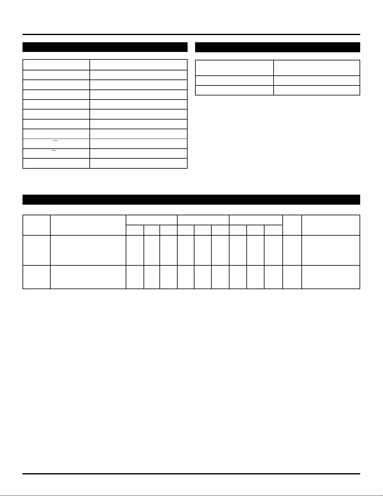
PIN NAMES
Pin Function
D0–D11 Data Inputs
S-IN Serial Data Input
EN Enable, active LOW
HOLD Hold, active LOW
SHIFT Shift, active HIGH
CLK1, CLK2 Clock Inputs
R Reset Input
Q, Q Direct Output
Y, Y Register Output
CCO VCC to Output
V
TRUTH TABLE
Number of Output
HIGH Inputs Q
Even LOW
Odd HIGH
DC ELECTRICAL CHARACTERISTICS
VEE = VEE (Min.) to VEE (Max.); VCC = VCCO = GND
TA = 0°CTA = +25°CTA = +85°C
Symbol Parameter Min. Typ. Max. Min. Typ. Max. Min. Typ. Max. Unit Condition
IH Input HIGH Current µA—
I
CLK1, CLK2 ——200——200——200
R — — 300 — — 300 — — 300
All Other Inputs — — 150 — — 150 — — 150
EE Power Supply Current mA —
I
10E — 82 98 — 82 98 — 82 98
100E — 82 98 — 82 98 — 94 113
2
 Loading...