

MICREL SY10E154, SY100E154 Datasheet
5-BIT 2:1
MUX-LATCH
SY10E154
SY100E154
FEATURES
■ 750ps max. LEN to output
■ Extended 100E VEE range of –4.2V to –5.5V
■ 700ps max. D to output
■ Differential outputs
■ Asynchronous Master Reset
■ Dual latch-enables
■ Fully compatible with industry standard 10KH,
100K ECL levels
■ Internal 75KΩ input pulldown resistors
■ Fully compatible with Motorola MC10E/100E154
■ Available in 28-pin PLCC package
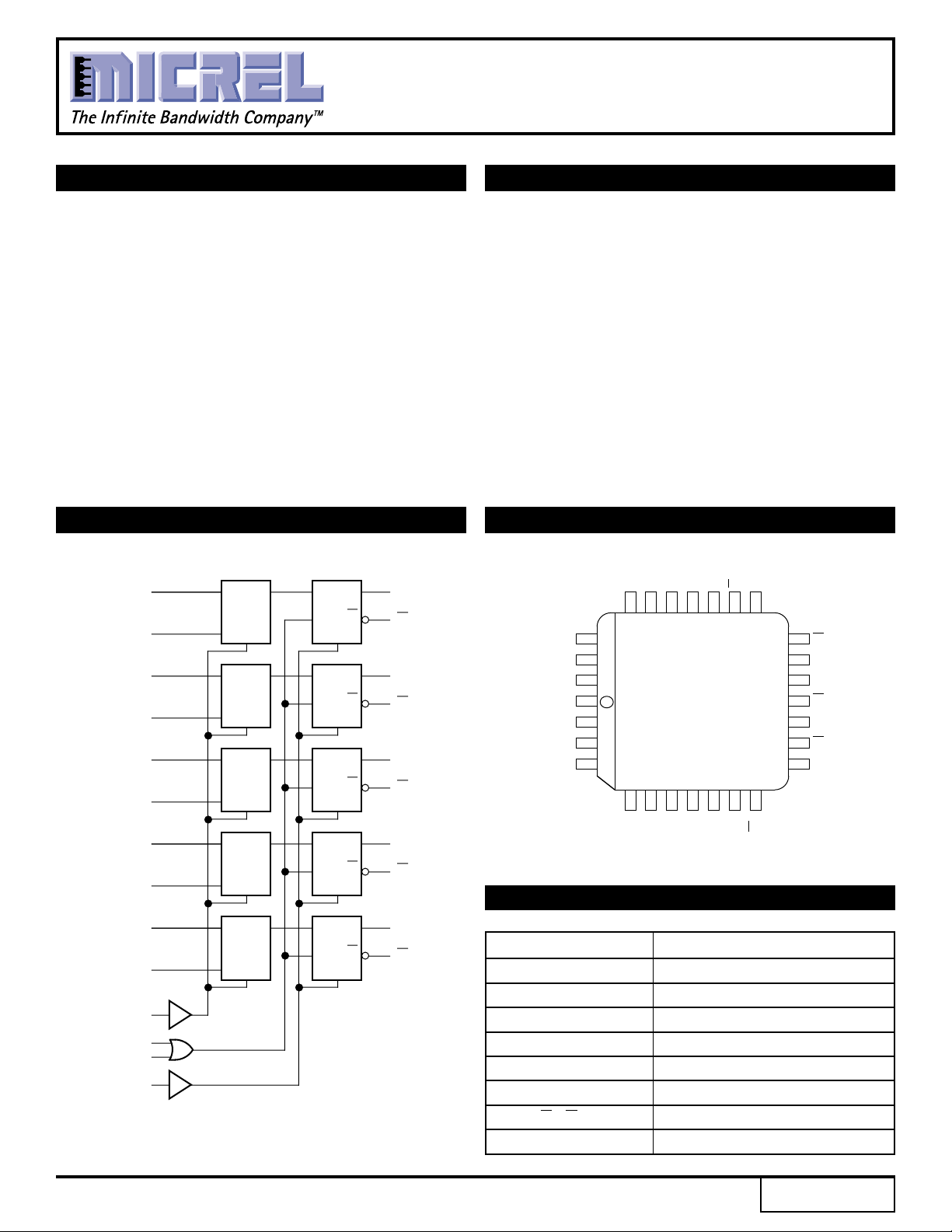
BLOCK DIAGRAM
D
D
D
D
D
D
D
D
D
D
SEL
LEN
LEN
MR
0a
MUX
0b
1a
SEL
MUX
1b
2a
SEL
MUX
2b
3a
SEL
MUX
3b
4a
SEL
MUX
4b
1
2
SEL
D
ENQ
R
D
E
N
R
D
E
N
R
D
E
N
R
D
E
N
R
Q
Q
Q
Q
Q
Q
Q
Q
Q
Q
0
Q
0
Q
1
Q
1
Q
2
Q
2
Q
3
Q
3
Q
4
Q
4
DESCRIPTION
The SY10/100E154 offer five 2:1 multiplexers followed
by latches with differential outputs, designed for use in
new, high-performance ECL systems. The two external
Latch-Enable signals (LEN1, LEN2) are gated through a
logical OR operation before use as control for the five
latches. When both LEN1 and LEN2 are at a logic LOW, the
latches are transparent, thus presenting the data from the
multiplexers at the output pins. If either LEN1 or LEN2 (or
both) are at a logic HIGH, the outputs are latched.
The multiplexer operation is controlled by the SEL(Select)
signal which selects one of the two bits of input data at each
mux to be passed through.
The MR (Master Reset) signal operates asynchronously
to make all Q outputs go to a logic LOW.
PIN CONFIGURATION
4
CCO
V
CCO
V
4
Q
Q
18
Q
3
17
Q
3
16
V
CC
Q
15
14
13
12
0
0
Q
Q
2
Q
2
Q
1
Q
1
SEL
LEN
LEN
V
MR
D
D
EE
4b
4a
3b
D
D
D3aD
25 24 23 22 21 20 19
26
1
27
2
28
1
2
0a
3
0b
4
567891011
1b
1a
D
D
PLCC
TOP VIEW
J28-1
2a
D2bD
PIN NAMES
Pin Function
D0a–D4a Input Data a
D0b–D4b Input Data b
SEL Data Select Input
LEN1, LEN2 Latch Enables
MR Master Reset
Q0–Q4 True Outputs
Q0–Q4 Inverted Outputs
CCO VCC to Output
V
Rev.: C Amendment: /1
1
Issue Date: February, 1998
Micrel
TRUTH TABLES
SY10E154
SY100E154
SEL Data
Ha
Lb
LEN1 LEN2 Latch
L L Transparent
H X Latched
X H Latched
DC ELECTRICAL CHARACTERISTICS
VEE = VEE (Min.) to VEE (Max.); VCC = VCCO = GND
TA = 0°CTA = +25°CTA = +85°C
Symbol Parameter Min. Typ. Max. Min. Typ. Max. Min. Typ. Max. Unit Condition
IIH Input HIGH Current ——150 ——150 ——150 µA —
EE Power Supply Current mA —
I
10E — 76 91 — 76 91 — 76 91
100E — 76 91 — 76 91 — 87 105
AC ELECTRICAL CHARACTERISTICS
VEE = VEE (Min.) to VEE (Max.); VCC = VCCO = GND
TA = 0°CTA = +25°CTA = +85°C
Symbol Parameter Min. Typ. Max. Min. Typ. Max. Min. Typ. Max. Unit Condition
PLH Propagation Delay to Output ps —
t
tPHL D 325 500 700 325 500 700 325 500 700
SEL 475 650 925 475 650 925 475 650 925
LEN 350 500 750 350 500 750 350 500 750
MR 450 600 800 450 600 800 450 600 800
S Set-up Time ps —
t
D 300 100 — 300 100 — 300 100 —
SEL 500 250 — 500 250 — 500 250 —
t
H Hold Time ps —
D300–100 — 300 –100 — 300 –100 —
SEL 200 –250 — 200 –250 — 200 –250 —
tRR Reset Recovery Time 800 600 — 800 600 — 800 600 — ps —
tPW Minimum Pulse Width, MR 400 ——400 ——400 ——ps —
tskew Within-Device Skew — 50 ——50 ——50 — ps 1
r Rise/Fall Time 300 475 800 300 475 800 300 475 800 ps —
t
tf 20% to 80%
NOTE:
1. Within-device skew is defined as identical transitions on similar paths through a device.
PRODUCT ORDERING CODE
Ordering Package Operating
Code Type Range
SY10E154JC J28-1 Commercial
SY10E154JCTR J28-1 Commercial
SY100E154JC J28-1 Commercial
SY100E154JCTR J28-1 Commercial
2
 Loading...