

MICREL MICRF003BM Datasheet
MICRF003 / 033
QwikRadiotm 900 MHz UHF Receiver
Preliminary Information
General Description
The MICRF003 is a single chip OOK (ON-OFF Keyed) Receiver IC for
remote wireless applications, employing Micrel’s latest QwikRadiotm
technology. This device is a true “antenna-in, data -out” monolithic device. All
RF and IF tuning is accomplished automatically within the IC, which
eliminates manual tuning, and reduces production costs. Receiver functions
are completely integrated. The result is a highly reliable yet extremely low
cost solution for high volume wireless applications. Because the MICRF003
is a true single-chip radio receiver, it is extremely easy to apply, minimizing
design and production costs, and improving time to market.
The MICRF003 provides two fundamental modes of operation, FIXED and
SWP. In FIXED mode, the device functions like a conventional
Superheterodyne receiver, with an (internal) local oscillator fixed at a single
frequency based on an external reference crystal or clock. As with any
conventional superheterodyne receiver, the transmit frequency must be
accurately controlled, generally with a crystal or SAW (Surface Acoustic
Wave) resonator.
In SWP mode, the MICRF003 sweeps the (internal) local oscillator at rates
greater than the baseband data rate. This effectively “broadens” the RF
bandwidth of the receiver to a value equivalent to conventional superregenerative receivers. Thus the MICRF003 can operate with less
expensive LC transmitters without additional components or tuning, even
though the receiver topology is still superheterodyne. In this mode the
reference crystal can be replaced with a less expensive ± 0.5% ceramic
resonator.
The MICRF003 provides two additional key features: (1) a Shutdown Mode,
which may be used for duty-cycle operation, and (2) a “Wakeup” function,
which provides a logical indication of an incoming RF signal. These features
make the MICRF003 ideal for low and ultra-low power applications, such as
RKE and RFID.
All post-detection (demodulator) data filtering is provided on the MICRF003,
so no external filters need to be designed. Any one of four filter bandwidths
may be selected externally by the user. Nominal filter bandwidths range in
binary steps, from 0.75kHz to 6kHz (SWP mode) or 2.8kHz to 22.4kHz
(FIXED mode). The user only needs to program the appropriate filter
selection based on data rate and code modulation format.
Features
• Complete 900 MHz Band receiver on a monolithic IC
• UHF Frequency range 800 to 1000 MHz
• Typical range over 170 meters with monopole antenna
• Data rates to 5kbps (SWP), 20kbps (FIXED)
• Automatic tuning, no manual adjustment
• No Filters or Inductors required
• Low Operating Supply Current--4mA @ 868MHz
• Shutdown Mode for Duty-Cycle Operation in excess of
100:1
• Wakeup Function to Enable External Decoders and
Microprocessors
• Very low RF re-radiation at the antenna
• CMOS logic interface to standard decoder and
microprocessor ICs
• Extremely low external part count
Applications
• Automotive Remote Keyless Entry
• Security Systems
• Low Rate Data Modems
• Remote Meter Data Collection
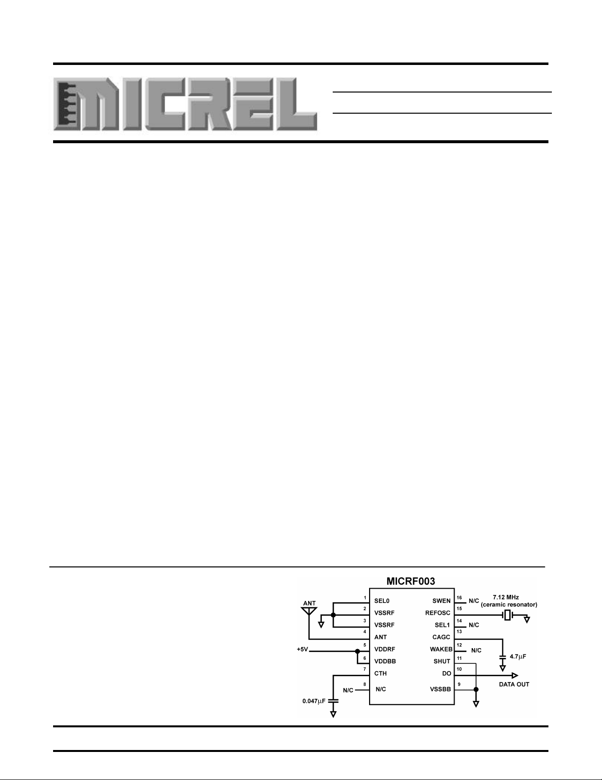
Typical Operating Circuit
915 MHz, 2400 bps OOK
ISM Band RECEIVER
Micrel Inc. • 1849 Fortune Drive San Jose, Ca 95131 • USA • tel + 1 (408) 944-0800 • fax + 1 (408) 944-0970 • http://www.micrel.com
MICRF003 Micrel
QwikRadio
tm
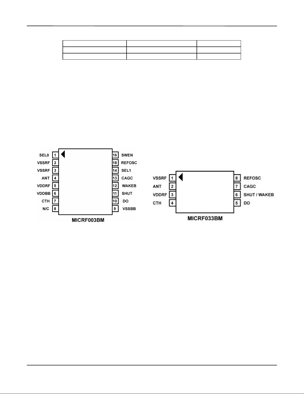
Ordering Information
Part Number Temperature Range Package
MICRF003BM
MICRF033BM
The standard 16-pin package provides the user with complete control of MICRF002 mode and filter selection. An 8-pin
standard part is also available for very low cost applications. The 8-pin version comes pre-programmed in SWP mode, with
Demodulator Filter bandwidth set to 5000Hz, and SHUT pin externally available. Other 8-pin configurations are available.
Contact the factory for details.
-40°C to +105°C
-40°C to +105°C
16-Pin SOIC
8-Pin SOIC
Pin Configuration (SOIC)
October 1999 MICRF003
2

MICRF003 Micrel
QwikRadio
tm
Pin Description (Pin numbers for the 8-pin version are identified in parentheses)
Pin Number Pin Name Pin Function
1 SEL0 This pin, in conjunction with SEL1, programs the desired Demodulator Filter Bandwidth. This pin is internally
2/3
(1)
4
(2)
5
6 VDDBB This pin is the positive supply input for the baseband section of the IC. VDDBB and VDDRF should be
(3) VDDRF This pin is the positive supply input for the IC. Connect a low ESL, low ESR decoupling capacitor from this pin
7
(4)
8 N/C Unused Pin
9 VSSBB This is the ground return for the baseband section of the IC. The bypass and output capacitors connected to
10
(5)
11
(6)
12 WAKEB An output signal, active low when the IC detects an incoming RF signal, determined by monitoring for data
13
(7)
14 SEL1 This pin, in conjunction with SEL0, programs the desired Demodulator Filter Bandwidth. This pin in internally
15
(8)
16 SWEN This logic pin controls the operating mode of the MICRF003. When SWEN = HIGH, the MICRF003 is in SWP
VSSRF This pin is the ground return for the RF section of the IC. The bypass capacitor connected from VDDRF to
VSSRF This pin is the ground return for the IC. The bypass capacitor connected from VDDRF to VSSRF should have
ANT This is the receive RF input, internally ac-coupled. Connect this pin to the receive antenna. Input impedance is
VDDRF This pin is the positive supply input for the RF section of the IC. VDDBB and VDDRF should be connected
CTH This capacitor extracts the (DC) average value from the demodulated waveform, which becomes the reference
DO The output data signal. CMOS level compatible.
SHUT A logic input for Shutdown Mode control. Pull this pin low to place the IC into operation. This pin in internally
CAGC Integrating capacitor for on-chip AGC (Automatic Gain Control). The Decay/Attack time-constant (TC) ratio is
REFOSC This is the timing reference for on-chip tuning and alignment. Connect either a ceramic resonator or crystal
SEL0 SEL1 Demodulator Bandwidth (Hz)
1 1 6000 22400
0 1 3000 11200
1 0 1500 5600
0 0 750 2800
pulled-up to VDDRF. See Table 1.
VSSRF should have the shortest possible lead length. For best performance, connect VSSRF to VSSBB at the
power supply only (i.e., keep VSSBB currents from flowing through VSSRF return path).
the shortest possible lead length.
high (FET gate) with approximately 2pF of shunt (parasitic) capacitance. For applications located in high
ambient noise environments, a fixed value band-pass network may be connected between the ANT pin and
VSSRF to provide additional receive selectivity and input overload protection. (See “Application Note TBD”.)
directly at the IC pins. Connect a low ESL, low ESR decoupling capacitor from this pin to VSSRF, as short as
possible.
connected directly at the IC pins.
to VSSRF, as short as possible.
for the internal data slicing comparator. Treat this as a low-pass RC filter with source impedance of nominally
90kohms ( for REFOSC frequency Ft = 6.75MHz, see “Application Note TBD”). A standard ± 20% X7R
ceramic capacitor is generally sufficient.
VSSBB should have the shortest possible lead lengths. For best performance, connect VSSRF to VSSBB at
the power supply only (i.e., keep VSSBB currents from flowing through VSSRF return path).
pulled-up to VDDRF.
preamble. CMOS level compatible.
nominally set as 10:1. Use of 0.47uF or greater is strongly recommended for best range performance. Use
low-leakage type capacitors for duty-cycle operation (Dip Tantalum, Ceramic, Polyester). (See “Application Note
TBD.)
pulled-up to VDDRF. See Table 1.
(mode dependent) between this pin and VSSBB, or drive the input with an AC coupled 0.5Vpp input clock. Use
ceramic resonators without integral capacitors. Note that if operating in FIXED mode, a crystal must be used;
however in SWP mode, one may use either a crystal or ceramic resonator. See “Application Note TBD” for
details on frequency selection and accuracy.
mode. When SWEN = LOW, the device operates as a conventional single-conversion superheterodyne
receiver. (See “Application Note TBD” for details.) This pin is internally pulled-up to VDDRF.
SWP Mode FIXED Mode
Table 1
Nominal Demodulator (Baseband) Filter Bandwidth
vs. SEL0, SEL1 and Mode
October 1999 MICRF003
3
MICRF003 Micrel
QwikRadio
tm
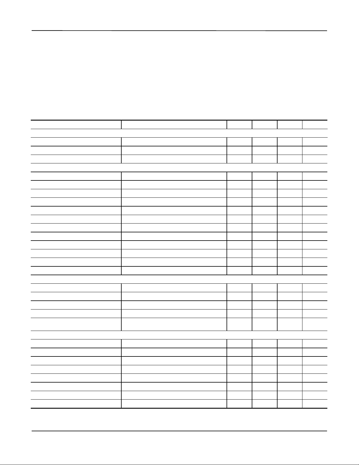
ABSOLUTE MAXIMUM RATINGS
Supply Voltage (VDDRF, VDDBB)..................................+7V
Voltage on any I/O Pin.........................VSS-0.3 to VDD+0.3
Junction Temperature...............................................+150°C
Storage Temperature Range......................-65°C to + 150°C
Lead Temperature (soldering, 10 seconds)..............+ 260°C
Operating Ratings
Supply Voltage (VDDRF, VDDBB)....................4.75V to
5.5V
Ambient Operating Temperature (TA)..........-40°C to
+105°C
Package Thermal Resistance θja (8 Pin SOIC).....120°C/W
Package Thermal Resistance θja (16 Pin SOIC).....120°C/W
Electrical Characteristics
Unless otherwise stated, these specifications apply for Ta = -40°C to 105°C, 4.75<VDD<5.5V. All voltages are with respect
to Ground; Positive currents flow into device pins. CAGC = 4.7µF, CTH = .047µF, VDDRF = VDDBB = VDD. REFOSC
frequency = 6.75MHz.
Parameter Test Conditions MIN TYP MAX UNITS
Power Supply
Operating Current 4 mA
Operating Current 10:1 Duty Cycle 400
Standby Current SHUT = VDD 1
RF/IF Section
Receiver Sensitivity Note 1, 3 -95 dBm
IF Center Frequency Note 4 2.37 MHz
IF 3dB Bandwidth Note 3, 4 1.18 MHz
Receive Data Rate FIXED Mode, Manchester Encoded Data 20 kbps
Receive Data Rate SWP Mode, Manchester Encoded Data 5 kbps
RF Input Range 800 1000 MHz
Receive Modulation Duty-Cycle 20 80 %
Maximum Receiver Input
Spurious Reverse Isolation
AGC Attack / Decay ratio T(Attack) / T(Decay) 0.1
AGC Leakage Current
Local Oscillator Stabilization Time To 1% of Final Value 2.5 msec
Demod Section
CTH Source Impedance Note 5 90k
CTH Source Impedance Variation -15 +15 %
CTH Leakage Current
Demod Filter Bandwidth SEL0 = SEL1 = SWEN = VDD, Note 4, 6 5730 Hz
Demod Filter Bandwidth SEL0 = SEL1 = VDD, SWEN = VSS,
Digital/Control Section
REFOSC Input Impedance 200k
Input Pullup Current SEL0, SEL1, SWEN, SHUT=VSS 8 µA
Input High Voltage SEL0, SEL1, SWEN 0.8VDD V
Input Low Voltage SEL0, SEL1, SWEN 0.2VDD V
Output Current DO, WAKEUP pins, Push-Pull 35 µA
Output High Voltage DO, WAKEUP pins, Iout = -1µA 0.9VDD V
Output Low Voltage DO. WAKEUP pins, Iout = +1µA 0.1VDD V
Output Tr, Tf DO, WAKEUP pins, Cload=15pF 5 µsec
Rs = 50Ω
ANT pin, Rs = 50Ω Note 2
Ta = 85°C
Ta = 85°C
Note 4, 6
-20 dBm
30
21500 Hz
±200
±200
µA
µA
µVrms
nA
Ω
nA
Ω
October 1999 MICRF003
4

MICRF003 Micrel
Note 1: Sensitivity is defined as the average signal level measured at the input necessary to achieve 10e-2 Bit Error Rate (BER). The input
signal is defined as a return-to-zero (RZ) waveform with 50% average duty cycle (e.g., Manchester Encoded Data) at a data rate of
600bps. The RF input is assumed to be matched into 50Ω.
Note 2: Spurious reverse isolation represents the spurious components which appear on the RF input (ANT) pin measured into 50Ω with an
input RF matching network.
Note 3: Sensitivity, a commonly specified Receiver parameter, provides an indication of the Receiver’s input referred noise, generally input
thermal noise. However, it is possible for a more sensitive receiver to exhibit range performance no better than that of a less
sensitive receiver, if the “ether” noise is appreciably higher than the thermal noise. “Ether” noise refers to other interfering “noise”
sources, such as FM radio stations, pagers, etc.
A better indicator of achievable receiver range performance is usually given by its Selectivity, often stated as Intermediate Frequency
(IF) or Radio Frequency (RF) bandwidth, depending on receiver topology. Selectivity is a measure of the rejection by the receiver of
“ether” noise. More selective receivers will almost invariably provide better range. Only when the receiver selectivity is so high that
most of the noise on the receiver input is actually thermal will the receiver demonstrate sensitivity-limited performance.
Note 4: Parameter scales linearly with REFOSC frequency Ft. For any REFOSC frequency other than 6.75MHz, compute new parameter
value as the ratio [(REFOSC FREQ (in MHz)) / 6.75] * [Parameter Value @ 6.75MHz]. Example: For REFOSC Freq. Ft =
7.12MHz, [Parameter Value @ 7.12MHz] = (7.12 / 6.75) * [Parameter Value @ 6.75MHz].
Note 5: Parameter scales inversely with REFOSC frequency Ft. For any REFOSC frequency other than 6.75MHz, compute new parameter
value as the ratio [6.75 / (REFOSC FREQ (in MHz))] * [Parameter Value @ 6.75MHz]. Example: For REFOSC Freq. Ft =
7.12MHz, [Parameter Value @ 7.12MHz] = (6.75 / 7.12) * [Parameter Value @ 6.75MHz].
Note 6: Demod filter bandwidths are related in a binary manner, so any of the other (lower) nominal filter values may be derived simply by
dividing this parameter value by 2, 4, or 8 as desired.
QwikRadio
tm
October 1999 MICRF003
5
 Loading...