

MICREL MIC94031BM4, MIC94030BM4 Datasheet
MIC94030/94031 Micrel
S
D
G
SS
PCB heat sink
plane improves
heat dissipation
PCB traces
MIC94030/94031
TinyFET™ P-Channel MOSFET
Preliminary Information
General Description
The MIC94030 and MIC94031 are 4-terminal silicon gate
P-channel MOSFETs that provide low on-resistance in a very
small package.
Designed for high-side switch applications where space is
critical, the MIC94030/1 exhibits an on-resistance of typically
0.75Ω at 4.5V gate-to-source voltage. The MIC94030/1 also
operates with only 2.7V gate-to-source voltage.
The MIC94030 is the basic 4-lead P-channel MOSFET. The
MIC94031 is a variation that includes an internal gate pull-up
resistor that can reduce the system parts count in many
applications.
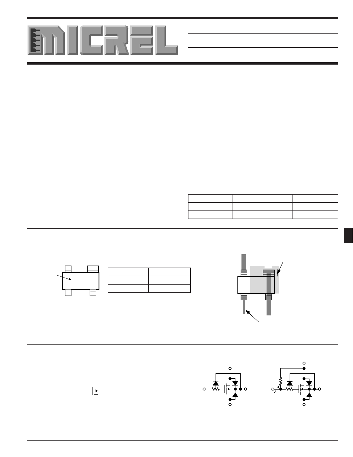
The 4-terminal SOT-143 package permits a substrate connection separate from the source connection. This 4-terminal
configuration improves the θJA (improved heat dissipation)
and makes analog switch applications practical.
The small size, low threshold, and low R
DS(on)
make the
MIC94030/1 the ideal choice for PCMCIA card sleep mode or
distributed power management applications.
Pin Configuration
Features
• 13.5V minimum drain-to-source breakdown
• 0.75Ω typical on-resistance
at 4.5V gate-to-source voltage
• 0.45Ω typical on-resistance
at 10V gate-to-source voltage
• Operates with 2.7V gate-to-source voltage
• Separate substrate connection for added control
• Industry’s smallest surface mount package
Applications
• Distributed power management
• PCMCIA card power management
• Battery-powered computers, peripherals
• Hand-held bar-code scanners
• Portable communications equipment
Ordering Information
Part Number Temperature Range* Package
MIC94030BM4 –55°C to +150°C SOT-143
MIC94031BM4 –55°C to +150°C SOT-143
* Operating Junction Temperature
Typical PCB Layout
6
Substrate
P3x
Part Number Identification
MIC94030BM4 P30
MIC94031BM4 P31
SourceGate
Identification
Part
Drain
SOT-143 Package (M4)
Schematic Symbol
Gate
Source
Substrate
Drain
Functional Diagrams
S
G
SS
D
~500kΩ
G
Internal
gate-to-source
pull-up resistor
S
SS
D
Schematic Symbol MIC94030 MIC94031
Patents 5,355,008; 5,589,702
1997 6-41
MIC94030/94031 Micrel
Absolute Maximum Ratings
Voltage and current values are negative. Signs not shown for clarity.
Drain-to-Source Voltage (pulse)....................................16V
Gate-to-Source Voltage (pulse) ....................................16V
Continuous Drain Current
TA = 25°C ....................................................................1A
TA = 100°C ...............................................................0.5A
Operating Junction Temperature ............... –55°C to +150°
Storage Temperature ...............................–55°C to +150°C
Total Power Dissipation
TA = 25°C ............................................................568mW
TA = 100°C ..........................................................227mW
Thermal Resistance
θ
...................................................................................... 220°C/W
JA
θ
..................................................................................... 130°C/W
JC
Lead Temperature
1/16" from case, 10s ........................................... +300°C
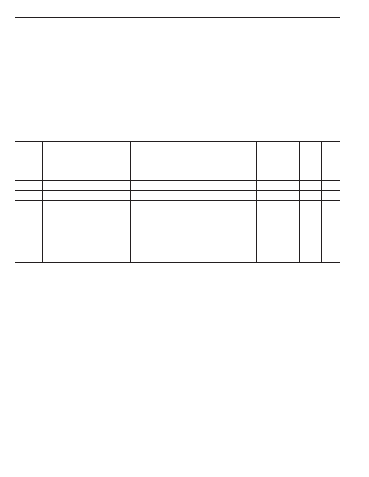
Electrical Characteristics
Symbol Parameter Condition (Note 1) Min Typ Max Units
V
BDSS
V
GS
I
GSS
R
GS
C
ISS
I
DSS
I
D(ON)
R
DS(ON)
g
FS
Note 1 T
Note 2 ESD gate protection diode conducts during positive gate-to-source voltage excursions.
Note 3 MIC94030 only
Note 4 MIC94031 only
Note 5 Pulse Test: Pulse Width ≤ 80µsec, Duty Cycle ≤ 0.5%
Drain-Source Breakdown Voltage VGS = 0V, ID = 250µA 13.5 V
Gate Threshold Voltage VDS = VGS, ID = 250µA 0.6 1.0 1.4 V
Gate-Body Leakage VDS = 0V, VGS = 12V, Note 2, Note 3 1 µA
Gate-Source Resistor VDS = 0V, VGS = 12V, Note 2, Note 4 500 750 1000 kΩ
Input Capacitance VGS = 0V, VDS = 12V 100 pF
Zero Gate Voltage Drain Current VDS = 12V, VGS = 0V 25 µA
On-State Drain Current VDS = 10V, VGS = 10V, Note 5 6.3 A
Drain-Source On-State Resist. VGS = 10V, ID = 100mA 0.45 Ω
Forward Transconductance VDS = 10V, ID = 200mA, Note 5 480 mS
= 25°C unless noted. Substrate connected to source for all conditions
A
Voltage and current values are negative. Signs not shown for clarity.
VDS = 12V, VGS = 0V, TJ = 125°C 0.010 250 µA
= 4.5V, ID = 100mA 0.75 1.00 Ω
V
GS
VGS = 2.7V, ID = 100mA 1.20 Ω
6-42 1997
 Loading...