

Page 1
Configurable PMIC, Five-Channel
HyperLight Load®, I2C Control and Enable
HyperLight Load is a registered trademark of Micrel, Inc.
Part Number
Description
C
D
F
G
E
A
B
General Description
MIC7401 Evaluation Board
Buck Regulator plus One-Boost with
Requirements
The MIC7401 is a powerful, highly-integrated,
configurable, power-m anagement IC (PMIC) featuring five
synchronous buck regulators, one boost regulator, and
high-speed I
2
C interface with an internal EEPROM and
micro-power shutdown. The device offers two distinct
modes of operation “standby mode” and “normal mode”.
In normal mode, the programmable switching converters
can be configured to support a variety of features,
including start-up sequencing, timing, soft-start ramp,
output voltage levels, current-limit levels, and output
discharge for each channel.
In standby mode the PM IC can configured in a low po wer
state by either disabling an output or by changing the
output voltage to a lower level. Independent exit from
standby mode can be achieved either by I
2
C
communication or the external STBY pin.
The initial settings of the evaluation board are:
Input: 2.4V to 5.5V
Output 1: 1.8V/0.8A Output 4: 1.05V/3.0A
Output 2: 1.1V/0.5A Output 5: 1.25V/1.0A
Output 3: 1.8V/0.5A Output 6: 12V/0.2A
The MIC7401 evaluation board requires only a single
power supply with 5A (minimum) current capability. The
output load can either be an active (electronic ) or passive
(resistive) load.
Precautions
The MIC7401 evaluation board does not have reverse
polarity protection. Applying a negative voltage to the VIN
and GND terminals can damage the device . The maximum
operating rating for V
is 5.5V. Exceed ing 5.5 V on the VIN
IN
could damage the device.
Ordering Information
MIC7401EV MIC7401 Evaluation Board
MICUSB USB Dongle
Datasheets and support documentation are available on
Micrel’s web site at: www.micrel.com
.
Evaluation Board
July 21, 2015
Micrel Inc. • 2180 Fortune Drive • San Jose, CA 95131 • USA • tel +1 (408) 944-0800 • fax + 1 (408) 474-1000 • http://www.micrel.com
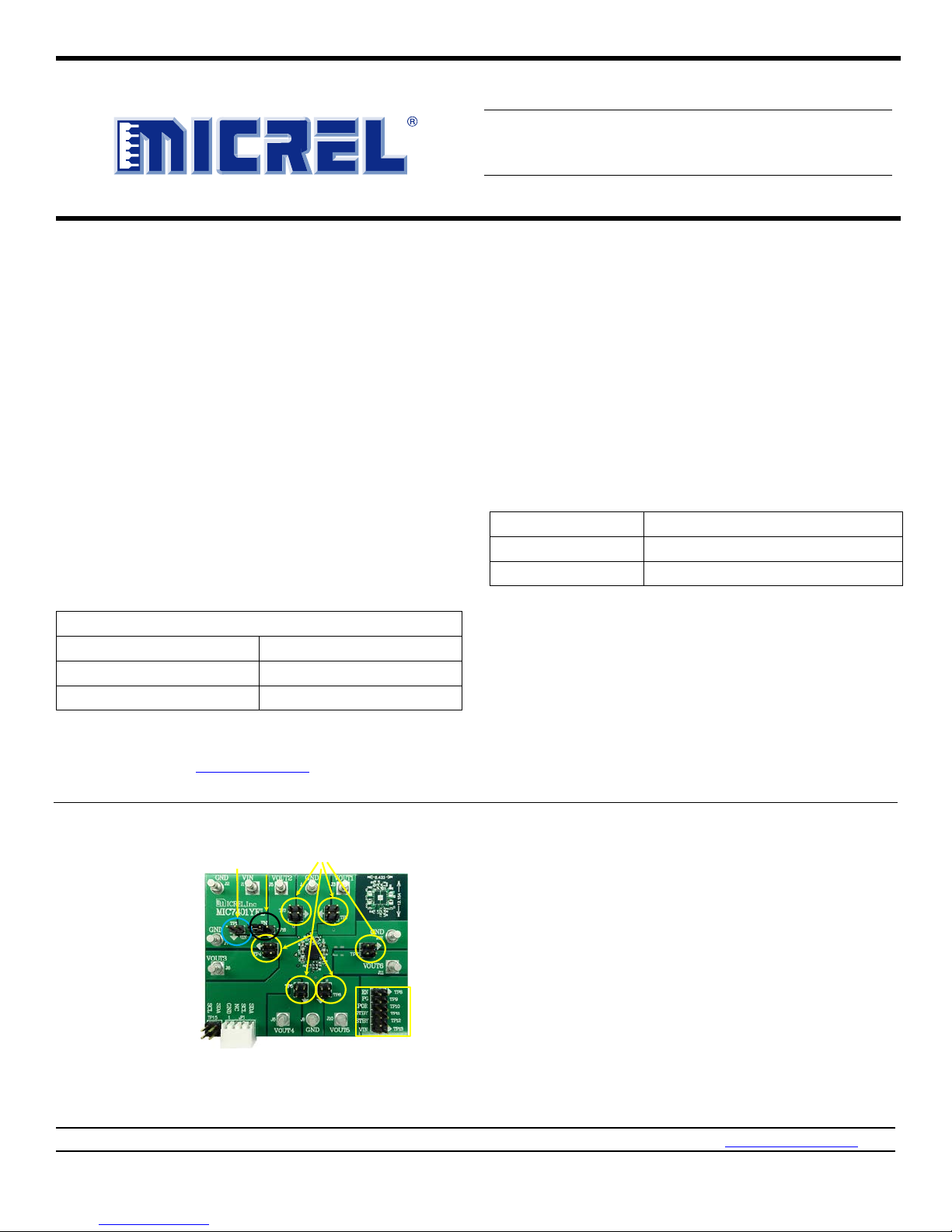
A) INPUT VOLTAGE
B) OUTPUT VOLTAGES
C) USB DONGLE CONNECTOR
2
D) I
C SDA AND SCL
E) I2C PULL-UP TO VIN
F) STATUS AND CONTROL BI T HEADER
G) ENABLE
Revision 1.0
Page 2
Micrel, Inc.
MIC7401 Evaluation Board
July 21, 2015
Test
Button
Save
Configuration
Target
OK
Getting Started
1. Download GUI
To download the GUI, select “Software Package/Kit”
from the MIC7401
website (www.micrel.com). Users can either save the
compressed installation file to hard drive or extract the
compressed file using a program such as PeaZip,
WinRAR, or WinZip. Then run MIC7401Install.msi to
install the GUI.
When the installation process is complete, click on the
Windows “Start” button, then select “All Programs” to
view the Start Menu. Find the new Micrel folder and
“click” on the Serial Programmer > MIC7401 to locate
the GUI program.
Before you launch the GUI, the USB dongle must be
connect to the PC by the USB cable, the USB dongle
plugged into the evaluation board and the board
powered up.
2. Set the USB Dongle and Switch Position
The USB dongle has a micro switch with two positions:
“I2C” and “NOM” (refer to Figure 1). To ensure the PC
is capable of communicating to the IC, confirm that the
micro switch is in the I
edge connector is the ground pin, which has a square
solder pad.
product page from the Micrel
2
C (or left) position. Pin 1 on the
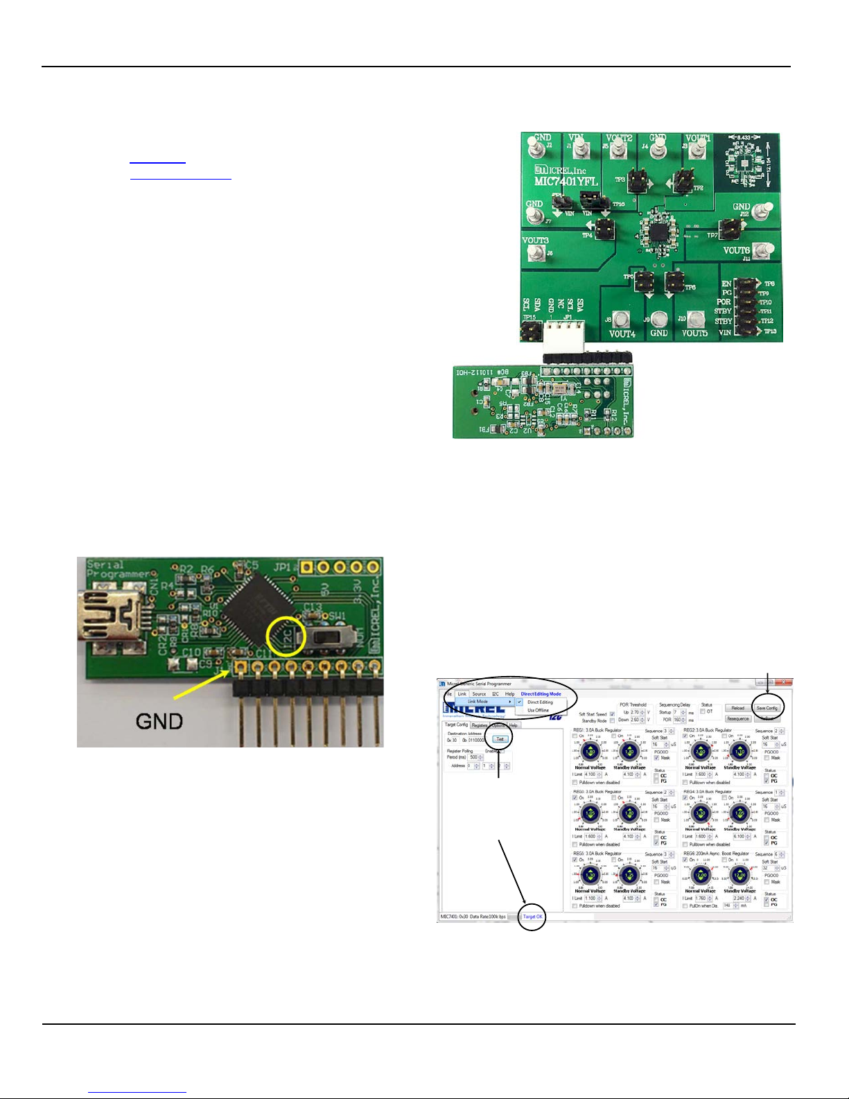
Figure 2. USB Dongle Connection to Evaluation Board
4. Configure the GUI for Direct Editing
When the MIC7401 GUI Interface window appears (see
Figure 3), the connection between the computer and the
USB dongle must be verified by clicking on the “Test”
button. “Target OK” will appear on the bottom of the G UI
window indicating it is oper ational. Before configuring the
MIC7401, the GUI nee ds to be set for dire ct edit ing . To do
this click on Link > Link Mode > Direc ting E ditin g. No w it is
time to program the MIC7401.
Figure 1. MIC7401 USB Dongle Micro Switch
3. Connect USB Dongle
The USB dongle is inverted and plugged into the 4-pin
socket (see Figure 2). Cutting off the extra pins is
recommended. Next, turn on the power supply and
slowly ramp up then input voltage. Now, click on the
MIC7400 ICON in the Start Menu to launch the GUI.
Figure 3. MIC7401 GUI Interface
2
Revision 1.0
Page 3
Micrel, Inc.
MIC7401 Evaluation Board
July 21, 2015
Evaluation Board Description
Programming Options
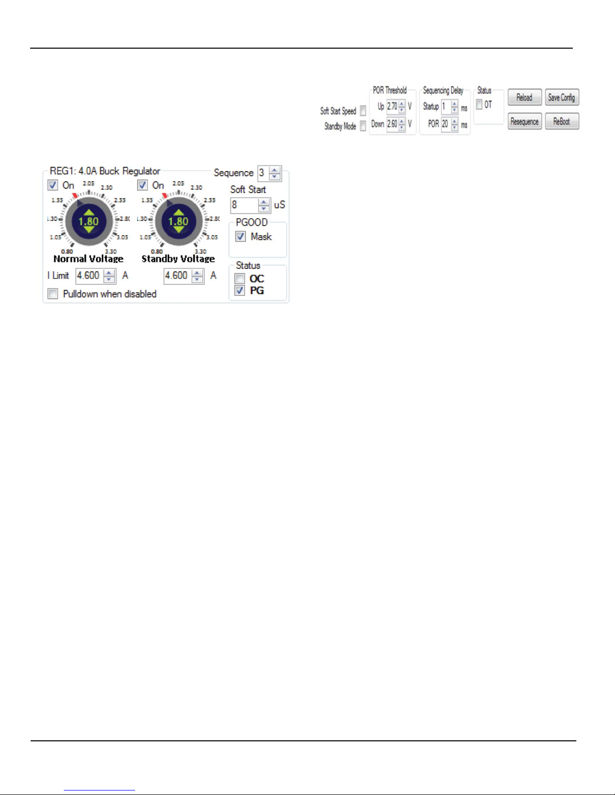
Every regulator has its own configuration settings that
allow the output voltage, current-limit, and soft-start ramp
rate to be set (Figure 4). The g lob al se tti ngs lik e po w er -onreset (POR) thresho ld and start-up delay are at the t op of
the MIC7401 GUI Interface window (Figure 5).
Figure 4. Regulator Settings
The first dial sets the outp ut voltage for normal mode and
the second sets standby mode. To change the voltage
setting, click on the up/down arrow or click and hold the
right mouse button on the pointer and drag the point er to
the desired voltag e level, then release the mous e button.
Note that the register associated with the output cha nges
on-the-fly every tim e the mouse is clicked. As th e voltage
level in the GUI changes, the output of the MIC7401 will
also change. The “On” check box is the ON/OFF control
for the regulators. If checked, the regulator is enabled.
Figure 5. Global Settings
The startup delay sets the delay between the internal
power good signal a nd the enable of the n ext regulator in
the sequence. The s equence setting allo ws the outputs to
come up in any order . There are six t ime slots. Each tim e
slot can be programmed for up to six regulators to be
turned on at once or none at all.
The MIC7401 can be powered up into either standby or
normal mode. The IC will start-up in standby mode if the
standby-mode check box is checked.
The soft-start speed check box when check ed set the soft
start ramp to the 8µs to 1024µs speed range. The OT
check box is a status indicator when c hecked indicate s an
overtemperature fault.
Evaluation Board
The MIC7401 evaluation board prov ides numerous two-pin
headers to monitor various system parameters such as
input voltage, output voltage, standby mode, and power
good. A standard test clip can be used, but for a more
elegant solution, use a tes t cable from Joy Signal PN: 9-
905305.
The soft-start ramp rate is registered in µs-per-step, with
each step being 50m V for the buck regul ators and 200m V
for the boost. It controls b oth the rising and falling rate of
the output voltage.
The PGOOD mask is used to control the global power
good output (PG). If this box is checked, then the output
will not contribute to the overall power good output. This
allows the output to go from normal mode to standby mode
without triggering a power good fault. Also the global
power good flag will not be affected by an over-current
fault.
The PG status box is checked when the output is within
91% of its regulated val ue. The OC status box indicates an
overcurrent condition.
In Figure 5, the POR threshold monitors A VIN a nd s ets the
lower and upper limit of the POR comparator. The POR
delay time starts as soon as AVIN vo ltage rises above the
upper threshold. The POR output goes low without delay
as soon as AVIN fall below the lower threshold limit.
3
Revision 1.0
Page 4
Micrel, Inc.
MIC7401 Evaluation Board
July 21, 2015
Functional Description
The MIC7401 is one of the industry’s most-advanced
PMIC devices designed for solid state drives (SSD) on the
market today. It is a multi-channel solution which offers
software configurable soft-start, sequencing, and digital
voltage control (DVC) that minimizes PC board area.
These features usually require a pin for programming.
However, this approach mak es the IC larger by increas ing
pin count, and also increases BOM cost due to the
external components.
The following is a complete list of the programmable
features of the MIC7401:
• Buck output voltage (0.8V – 3.3V/50mV steps)
• Boost output voltage (7.0V – 14V/ 200mV steps)
• Power-on-reset (2.25V – 4.25V/50mV steps)
• Power-on-reset delay (5ms – 160ms/5ms steps)
• Power-up sequencing (6 time slots)
• Power-up sequenc i ng de la y (0m s – 7ms/1ms steps)
• Soft-start (4µs – 1024µs per step)
• Buck current-limit threshold
− (1.1A to 6.1A/0.5A steps)
• Boost current-limit threshold
− (1.76A to 2.6A/0.12A steps)
• Boost pull-down (37mA to 148mA/37mA steps)
• Buck pull-down (90Ω)
• Buck standby output voltage programmable
• Boost standby output voltage programmable
• Global power-good masking
The MIC7401 has a current-m ode boost r egulator t hat can
deliver up to 200m A of output current and onl y consumes
70µA of quiescent current. The 2.0MHz switching
frequency allows small chip inductors to be used.
Programmable overcurrent sensing protects the boost
from overloads and an output disconnect switch opens to
protect against a short-circuit condition. Soft-start is also
programmable and controls both the rising and falling
output.
Programmable Buck Soft-Start Control
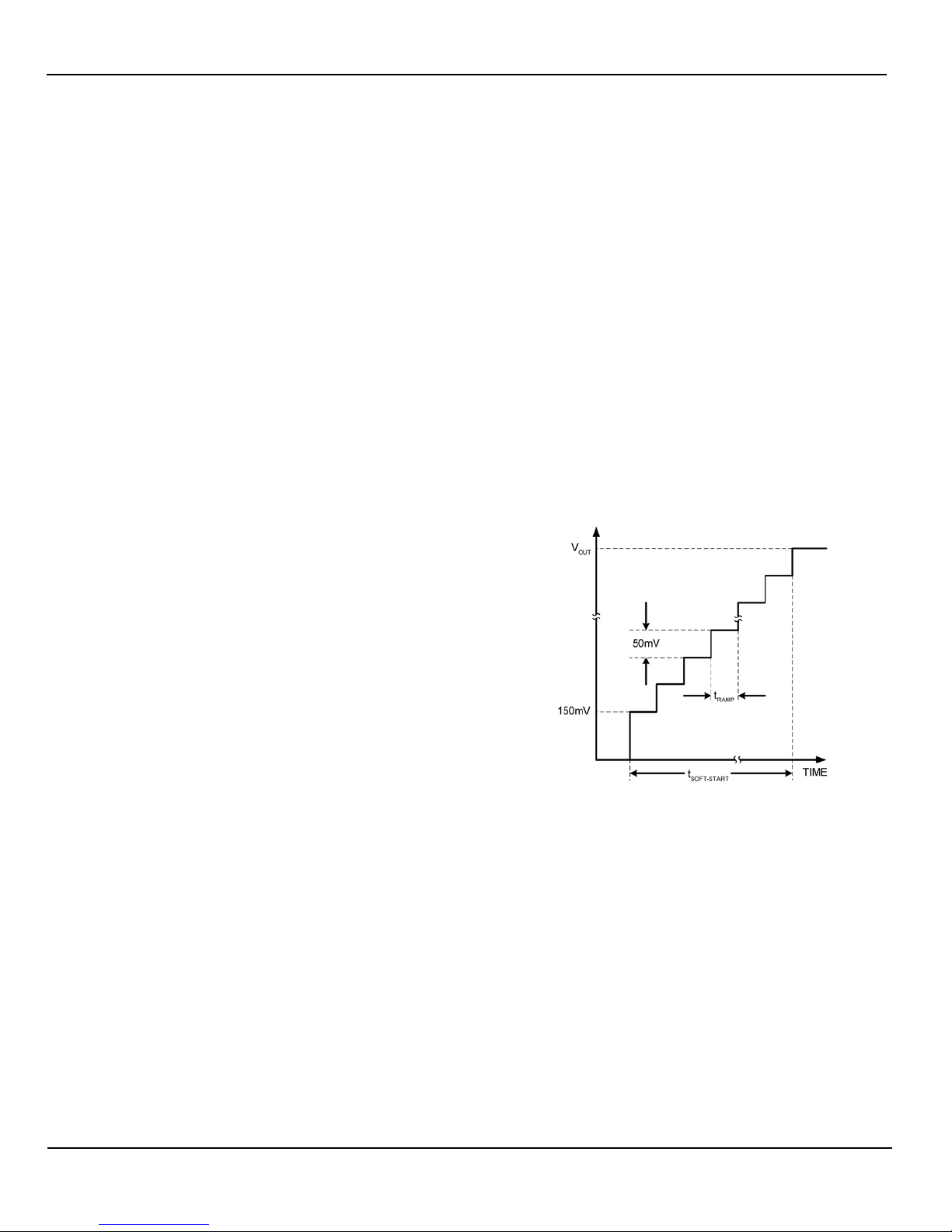
The MIC7401 soft-start feature forces the output voltag e to
rise gradually, which lim its the inrush current during startup. A slower output rise time will draw a l ower input surge
current. The s oft-start time is based on the leas t signif ic ant
bit (LSB) of an internal DAC and the speed of the ramp
rate, as shown in Figure 6. Figure 6 illustrates the soft-start
waveform for all five synchronous buck converters. The
initial step starts at 150mV and each subsequent step is
50mV.
These features give the system designer the flexibility to
customize the MIC7401 f or their application. For ex ample,
current lim it can be programmed to 4.1A and V
V
OUT1
OUT2
can be set to 1.1A. These outp uts can be programm ed to
come up at the sam e time or 2.0ms apart. In a ddition, in
power-saving standby mode, the outputs can either be
turned off or programmed to a lower voltage. With this
programmability the MIC7401 can be used in multiple
platforms.
The MIC7401 buck regulators are adaptive on-time
synchronous step-down DC-to-DC regulators. They are
designed to operate over a wide i nput voltage range from
2.4V to 5.5V and pro vide a regulated output voltage a t up
to 3.0A of output current. An adaptive on-time control
scheme is employed to obtain a constant switching
frequency and to simplify the control compensation. The
device includes an internal soft-start function which
reduces the power supply input surge current at start-up
by controlling the output voltage rise time.
Figure 6. Buck Soft-Start
The output ramp rate (t
) is set by the soft-start
RAMP
registers. Each output ramp rate can be individually set
from 4µs to 1024µs, see Table 1 for details.
4
Revision 1.0
Page 5
Micrel, Inc.
MIC7401 Evaluation Board
July 21, 2015
RAMP
OUT
SS
t
mV50
V15.0V
t ×
−
=
s264t
s8
mV50
V15.0V8.1
t
SS
SS
µ=
µ×
−
=
Table 1. Buck Outputs Default Soft-Start Time (DEFAULT)
V
V
1.8 8 264
OUT1
V
1.1 8 152
OUT2
V
1.8 8 264
OUT3
V
1.05 8 144
OUT4
VOUT5 1.25 8 176
OUT
(V)
t
RAMP
(µs)
tSS
(µs)
The soft-start time tSS can be calculated by Equation 1:
Eq. 1
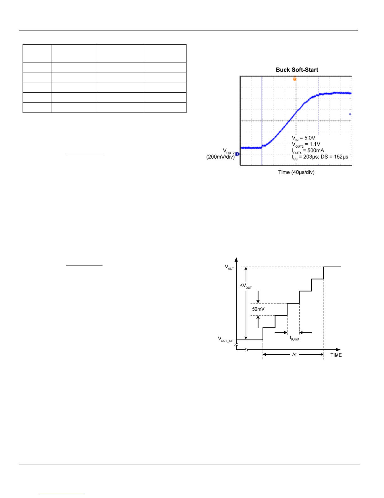
Figure 7 sho ws the output of Buck 1 ramping up c leanly,
starting from 0.15V to its final 1.1V value.
Where:
t
= Output rise time
SS
V
= Output voltage
OUT
t
= Output dwell time
RAMP
For example:
Where:
V
= 1.8V
OUT
t
= 8.0µs
RAMP
Figure 7. Buck Soft-Start
Buck Digital Voltage Control (DVC)
The output voltage has a 6-bit control DAC that can be
programmed from 0.8V to 3.3V in 50m V increments . If the
output is programm ed to a higher voltage, then t he output
ramps up, as shown in Figure 8.
Eq. 2
Figure 8. Buck DVC Control Ramp
5
Revision 1.0
Page 6
Micrel, Inc.
MIC7401 Evaluation Board
July 21, 2015
RAMP
INIT_OUTOUT
t
mV50
VV
t ×
−
=∆
The ramp time is determined by Equation 2:
Eq. 2
Where:
V
OUT_INIT
V
OUT
t
RAMP
= Initial output voltage
= Final output voltage
= Output dwell time
When the regulator is set in standby mode or progra mm ed
to a lower voltage, then th e output voltage ram ps down at
a rate determined by the output ramp rate (t
RAMP
), the
output capacitance and the external load. Small loads
result in slow output voltage deca y and heav y loads caus e
the decay to be controlled by the DAC ramp rate.
Programmable Boost Soft-Start Control
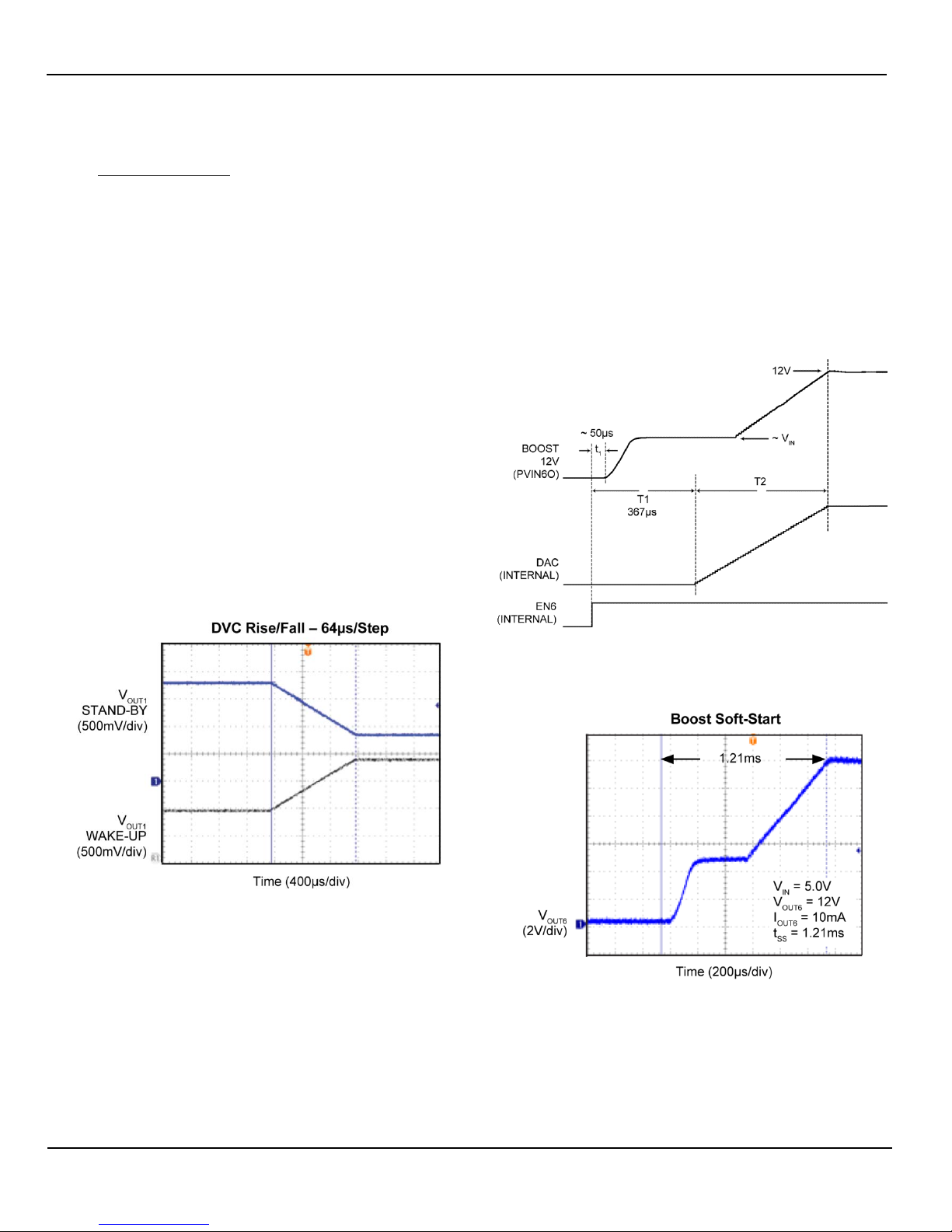
The boost soft-star t time is divided into t wo part s as s h o wn
in F igure 10. T1 is a fixed 367µs d elay starting f rom when
the internal enable goes high. This delay gives enough
time for the disconnect switch to turn on and bring the
inductor voltage to V
before the b oost is tur n ed on. There
IN
is a 50µs delay which is controlled by the parasitic
capacitance (Cgd) of the disconnect switch before the
output starts to rise.
After the T1 period, the DAC out put ramp starts, T2. The
total soft-start time, t
, is the sum of both periods. Figure
SS
11 displays the actual boost soft-start waveform.
In Figure 9 , V
is s witched to standby mode with an I² C
OUT1
command and then s witched back to normal m ode either
by an I²C command or a low-to-high transition of the ST BY
pin. In this case, the rise and f all times are the same due
to a 1A load on V
OUT1
.
Figure 9. Buck DVC Control Ramp
Figure 10. Boost Soft-Start Ramp
6
Figure 11. Boost Soft-Start
Revision 1.0
Page 7
Micrel, Inc.
MIC7401 Evaluation Board
July 21, 2015
( )
( )
s16
V2.0
V4.1V12
2T
t
V2.0
V4.1V
2T
2T1Tt
RAMP
OUT
SS
µ×
−
=
×
−
=
+=
RAMP
INIT_OUTOUT
t
V2.0
VV
t ×
−
=∆
The ramp time can be computed using Equation 4:
Eq. 3
Where:
T1 = 367µs
T2 = 848µs
t
= 367µs + 848µs = 1.215ms
SS
V
= Output voltage
OUT
t
= Output dwell time = 16µs
RAMP
Boost Digital Voltage Control (DVC)
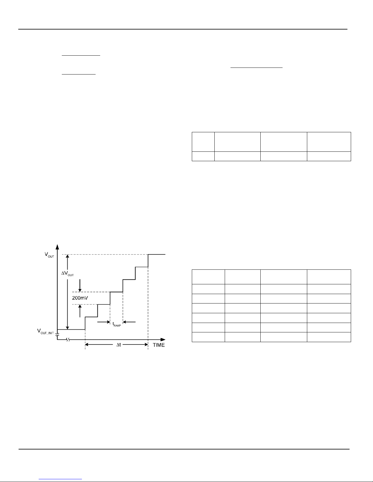
The boost output contro l works the sam e way as the buc k,
except that the voltag e steps are 200mV (see Figure 12).
When the boost is programmed to a lower voltage the
output ramps down at a rate determined by the output
ramp rate (t
), the output capacitanc e and the external
RAMP
load. During both the ramp up and down time, the po wergood output is blanked and will not imitate a fault flag.
Eq. 4
Where:
V
OUT_INIT
= Initial output voltage
Table 2. Boost Output Default Soft-Start Time
V
V
12 16 1.215
OUT6
OUT
(V)
t
RAMP
(µs)
tSS
(ms)
Buck Current Limit
The MIC7401 buck regulators have high-side current
limiting that can be varied by a 4-bit code. If t he regulator
remains in current limit for more than seven consecutive
PWM cycles, the output is latched off, the overcurrent
status register bit is set to 1, the power-good status
register bit is set to 0 and the global power-good (PG)
output pin is pulled low. An overcurrent f ault on one o utput
will not disable the rem aining outputs. Table 3 shows the
current-limit register settings vs. output current. The
current-limit register setting is set at twice the maximum
output current.
Figure 12. Boost DVC Control Ramp
Table 3. Buck Current-Limit Register Settings
I
I
OUT(MAX)
0.5A 1.1A 1111 F’h
1.0A 2.1A 1101 D’h
1.5A 3.1A 1011 B'h
2.0A 4.1A 1001 9'h
2.5A 5.1A 0111 7'h
3.0A 6.1A 0101 5'h
BINARY HEX
PROG
The output can be t urned back on by recycling the input
power or by software con trol. T o clear th e over current f ault
by software contro l, set the enable register bit to “ 0” then
clear the overcurrent fau lt by setting t he fault regis ter bit to
“0”. This will c lear the over-current and po wer-good status
registers. Now the out put can be re-enabled by setting the
enable register bit to “1”.
7
Revision 1.0
Page 8
Micrel, Inc.
MIC7401 Evaluation Board
July 21, 2015
During start-up sequencing if Output 1 is still shorted,
Outputs 2 through 4 will come up normally. Once an
overcurrent condition is sensed, then the fault register is
set to “1” and the start-up sequence will stop and no
further outputs will be enabled.
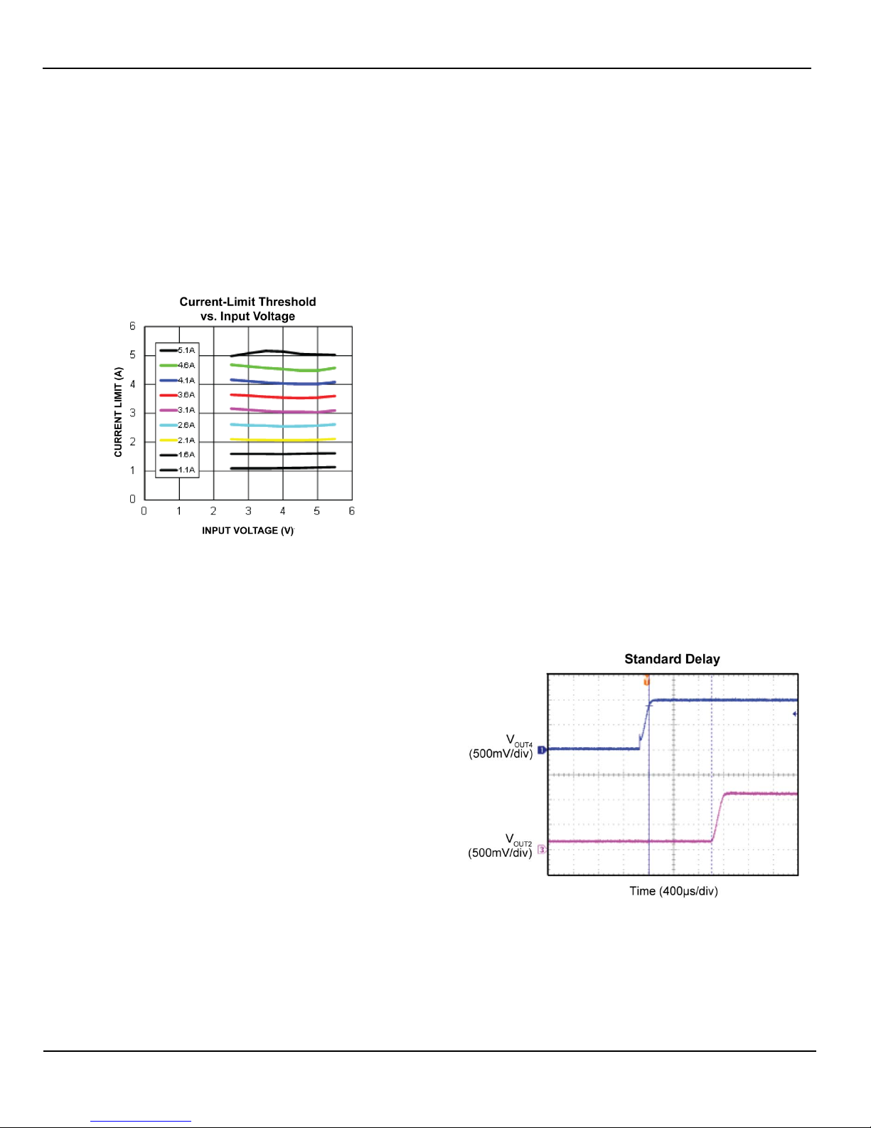
The programmable current-limit setting sets the peak
switch current threshold, not the average outputs current.
The peak current is higher than the average due to the
inductor ripple current. Figure 13 illustrates how the
current limit threshold varies with input voltage.
Figure 13. Current-Limit Threshold vs. Input Voltage
Boost Current Limit
The boost current lim it features cycle-by-cycle protec tion.
The duty cycle is c ut immediately once t he current limit is
hit. When the boost c urrent limit is hit f or five consecutive
cycles, the FAULT signal is asserted and remains asserted
with the boost converter k eepi ng on r unnin g until the boost
is powered off.
Global Power-Good Pin
The global power-good out put indic ates that all the out puts
are above the 91% limit after the power-up sequence is
completed. Once the power-up sequence is complete, the
global power good outpu t stays high un less an output falls
below its power-good lim it, a ther mal fault occurs, the i nput
voltage drops below the lower UVLO threshold or an
output is turned OFF by setting the enabl e register bit to
“0” unless the PGOOD_MASK[x] bit is set to “1” (Default).
A power-good mask bit c an be used to control the global
power-good output. The power-good mask feature is
programmed through t he PGOOD_MASK[x] registers and
is used to ignore an individual power-good fault. When
masked, PGOOD_MASK[x] bit is set to “1”, an individual
power good fault will not cause the global power good
output to de-assert.
If all the PGOOD_MASK[x] bits are set to “1”, then the
power good output de-ass erts as soon as the first output
starts to rise. The PGOO D_MASK[x] bit of the last output
must be set to “0” to h ave the PG ou tput stay l ow until the
last output reaches 91% of its final value.
The global power-good out put is an open-drain output. A
pull-up resistor can be connected to V
or V
IN
connect the pull-up resistor to a voltage higher than AV
. Do not
OUT
.
IN
Standard Delay
There is a programmable timer that is used to set the
standard delay time between each time slot. The timer
starts as soon as the previous time slot’s output power
good goes high. When the del ay com pletes, the regu lators
assigned to that time slot are enabled, see F i gure 14.
This protects the boost in normal overload conditions , but
not in a short-to-ground cas e. For a s hort c ircui t to gr ound ,
the boost current limit will not be ab le to limit the inductor
current. This short-circuit condition is sensed by the
current in the disconnect switch. When the disconnect
switch current lim it is hit for four cons ecutive master clock
cycles (2MHz), regard less if the boost is switc hing or not,
both the disconnect switch and boost are latched off
automatically and the FAULT signal is asserted.
The output can be t urned back on by recycling the input
power or by software con trol. T o clear th e over current f ault
by software contro l, set the enable register bit to “ 0” then
clear the overcurrent fau lt by setting t he fault regist er bit to
“0”.
Figure 14. Standard Delay Time
8
Revision 1.0
Page 9
Micrel, Inc.
MIC7401 Evaluation Board
July 21, 2015
Power-Up Sequencing
When power is first applied to the MIC7401, all I²C
registers are loaded with their default values from the
EEPROM. There is about a 1.5ms delay before the first
regulator is enabled while the MIC7401 goes through the
initialization process . The DELAY register’s STDEL bit s s et
the delay between powering up each regulator at initial
power up.
The sequencing registers allow the outputs to come up in
any order. There are six tim e slots that an output can be
configured to power up in. Each time slot can be
programmed for up to six regulators to be turned on at
once or none at all.
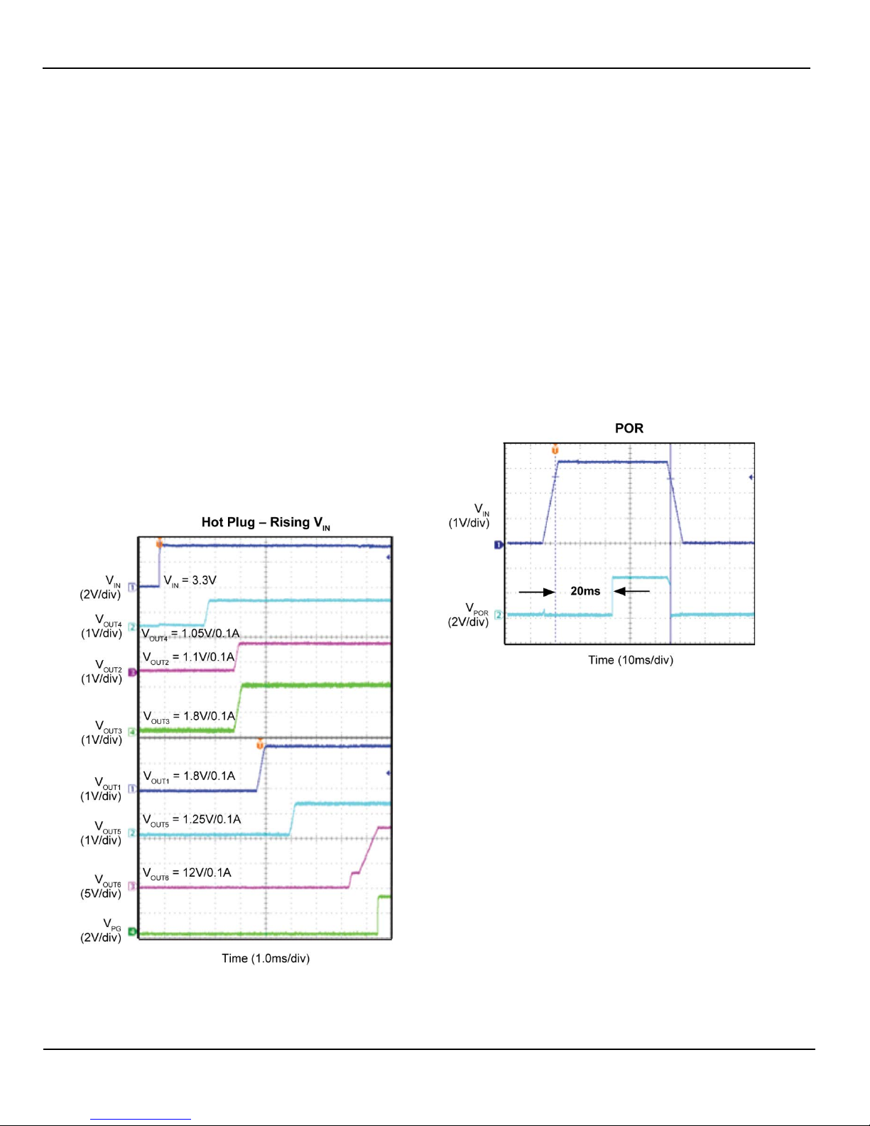
Figure 15 shows an example of this feature. V
enabled in time slot 1. Af ter a 1ms delay, V
OUT2
and V
OUT4
is
OUT3
are enable at the same time in tim e slot 2. The 1ms is the
standard delay for all of the outputs and can be
programmed from 0ms to 7ms in 1ms. Next, V
powered up in time s lot 3 and V
in tim e slot 4. There
OUT5
OUT1
is
are no regulators programmed for time slot 5. Finally,
is po wered up in time slot 6 . The global power-good
V
OUT6
output, V
, goes high as soon as the last o utput reaches
PG
91% of its final value.
Global Enable Pin
When the enable pin rises above the enable threshold
voltage, the MIC7401 enters its start-up sequence.
Programmable Power-on-Reset (POR) Delay
The POR output pin pro vides the user with a w ay to let the
SOC know that the input power is failing. If the input
voltage falls below the power-on reset lower threshold
level, the POR output immediately goes low. The lower
threshold is set in the PORDN register and the upper
threshold uses PORUP register.
The low-to-high POR transition can be delayed from 5ms
to 160ms in 5ms increm ents. This feature can be used to
signal the SOC that the power supplies are stable. The
PORDEL register sets the del ay of the POR pin. T he POR
delay starts as soon as the AVIN pin voltage rises a bove
the power-on-reset upper thr eshold limit. Figure 16 shows
the POR operation.
Figure 16. Power -on-Reset (POR)
Figure 15. Hot Plug – V
IN
Rising
9
Revision 1.0
Page 10
Micrel, Inc.
MIC7401 Evaluation Board
July 21, 2015
Timing Diagrams
Normal Power-Up Sequence for Outputs
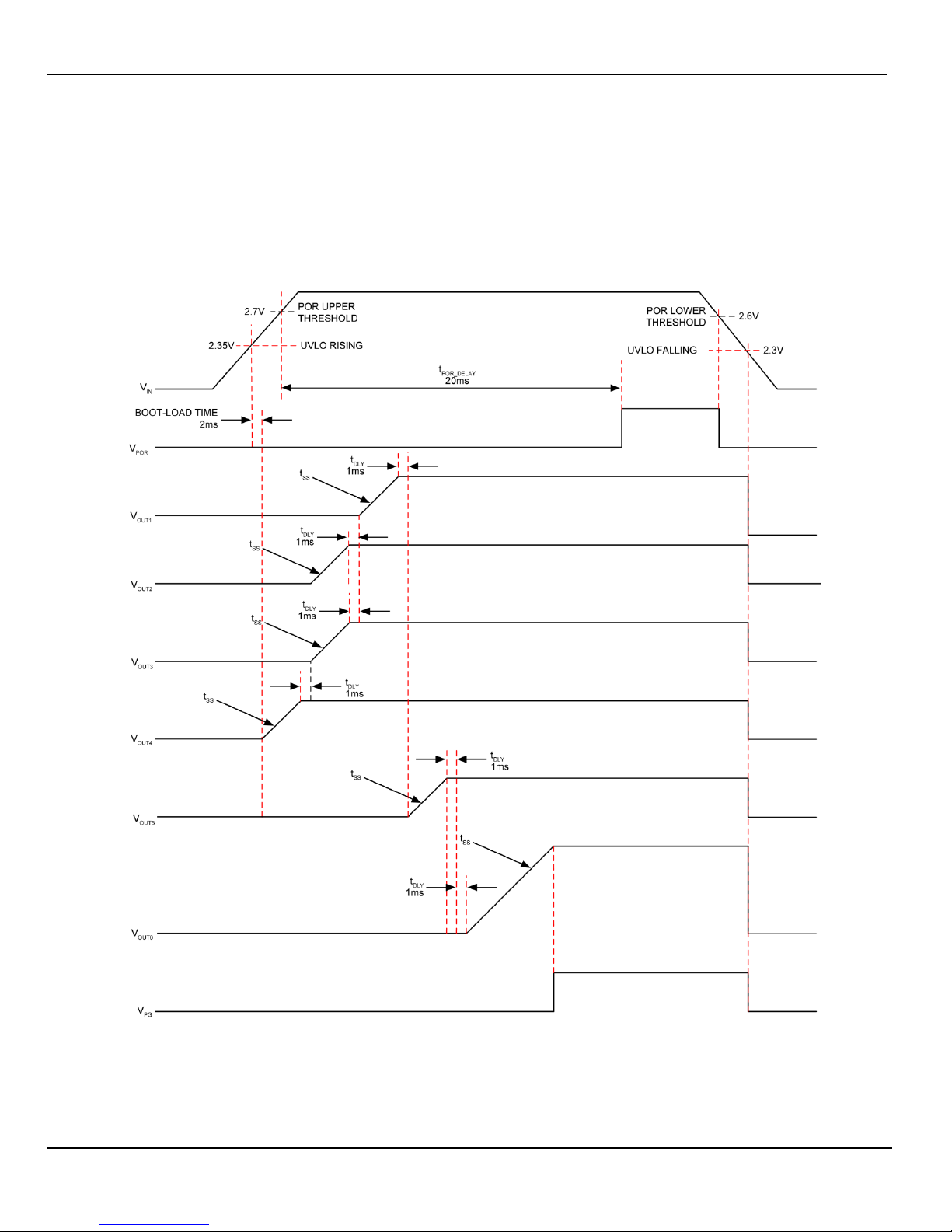
The STDEL register sets the delay between powering up
of each regulator at initial power-up (see power-up
sequencing in F igure 17). Once all the internal power-good
registers PGOOD[1-6] are all 1, then the global PG pin
goes high without dela y if the PGOOD_MAS K[6] bit is set
to “0”.
The PORDEL register sets the delay for the POR f lag pin.
The POR delay time starts as soon as AVIN pin voltage
rises above the system UVLO upper threshold set by the
PORUP register. The POR outp ut goes lo w w itho ut de l a y if
AVIN falls below the lower UVLO threshold set by the
PORDN register.
Figure 17. MIC7401 Power-Up/Down
10
Revision 1.0
Page 11
Micrel, Inc.
MIC7401 Evaluation Board
July 21, 2015
Standby (STBY) Pin (Wake-Up)
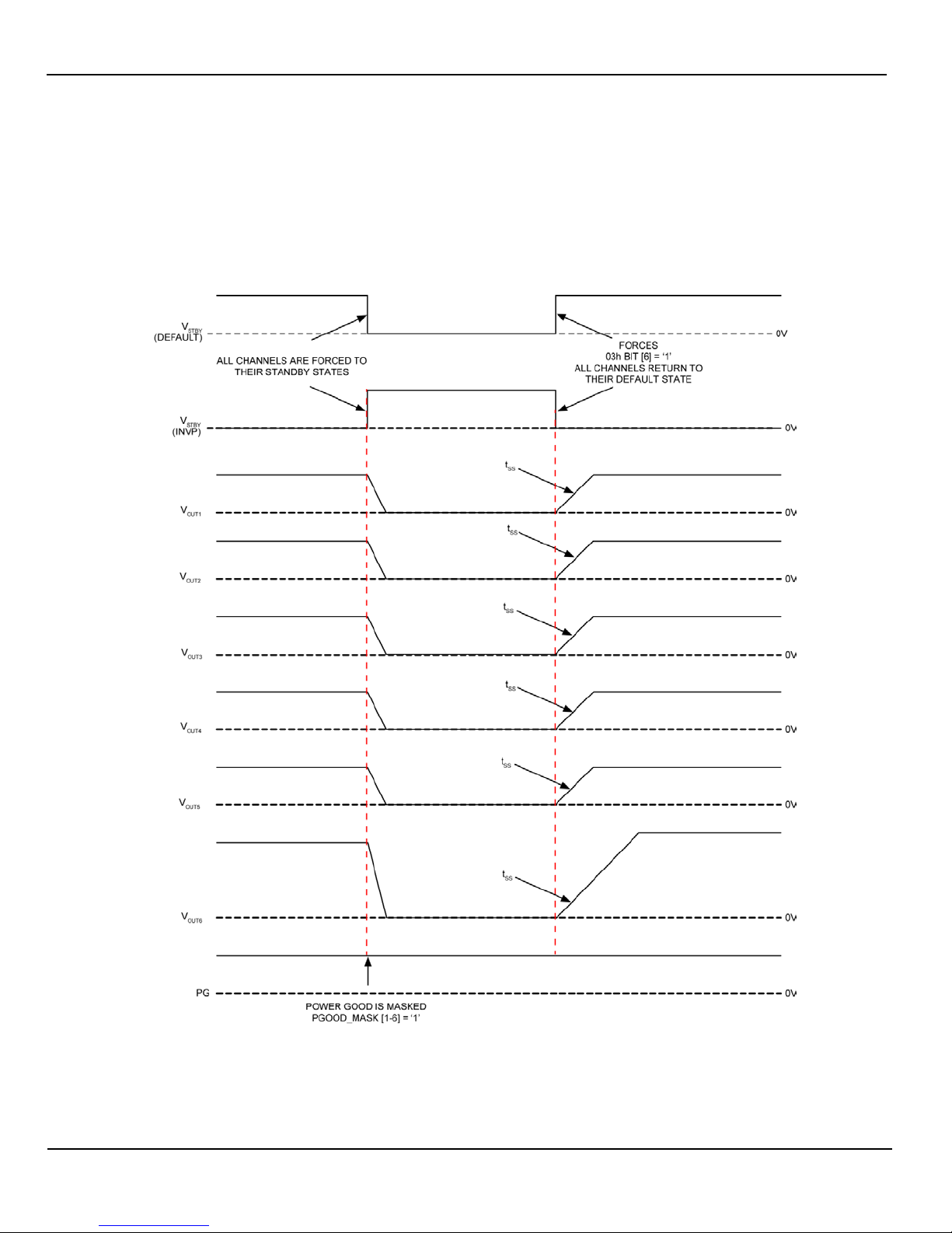
An I²C write command to the STBY_CTRL_REG register
or the STBY pin can be used to set the MIC7401 into
stand-by mode. The standby (STBY) pin provides a
hardware-specific m anner in which to wake-up from standby mode and go into normal mode. Figure 18 shows the
STBY pin operat ion. A low-to-high transition on the STBY
pin switches the output from stand-by mode to normal
mode.
There is a 100µs STBY deglitch time that eliminates
nuisance tripping, allowing all regulators to enable at the
same time and ramp up with their programmed ramp rates.
Figure 18. MIC7401 STBY Function (DEFAULT)
11
Revision 1.0
Page 12
Micrel, Inc.
MIC7401 Evaluation Board
July 21, 2015
SW4
OUT4
MIC7401
C1
2.2µF
PVIN1
L4
1.0µH
PGND4
C14
22µF
PVIN4
C13
10µF
SW3
OUT3
L3
2.2µH
PGND3
C12
22µF
PVIN3
C11
10µF
SW2
OUT2
L2
2.2µH
PGND2
C10
22µF
PVIN2
26
C9
10µF
L1
2.2µH
SW1
OUT1
PGND1
C3
22µF
C2
10µF
PVIN6
L6
2.2µH
PVIN6O
SW6
PGND6
C6
10µF
PVIN5
L5
2.2µH
SW5
OUT5
PGND5
C8
22µF
C7
10µF
31
30
AVIN
EN
15
14
13
POR
SCL
AGND
SDA
35
34
33
32
PG
NC
NC
AGND
12
STBY
16
R1
100kΩ
OUT6
C5
22µF
R6
499kΩ
D1
PMEG4002
27
29
28
25
24
23
22
21
20
19
17
18
2
1
3
36
4
5
7
6
8
9
11
10
R5
2kΩR32kΩR2100kΩ
CLK
SDA
NC
4
3
2
VIN
VIN
VIN
VIN
VIN
VIN
VIN
V
OUT1
1.8V/0.8A
V
OUT6
12V/0.2A
V
OUT5
1.25V/1.0A
V
OUT4
1.05V/3.0A
V
OUT3
1.8V/0.5A
V
OUT2
1.1V/0.5A
R7
0Ω
C4
10µF
PGND
PGND
PGND
GND
1
PGND
VIN
PGND
PGND
PGND
R4
499kΩ
VIN
EN
VIN
STAND
-
BY
STAND-BY
POR
PG
EN
VIN
PG
EN
VIN VOUT3
VOUT3
C15
150µF
+
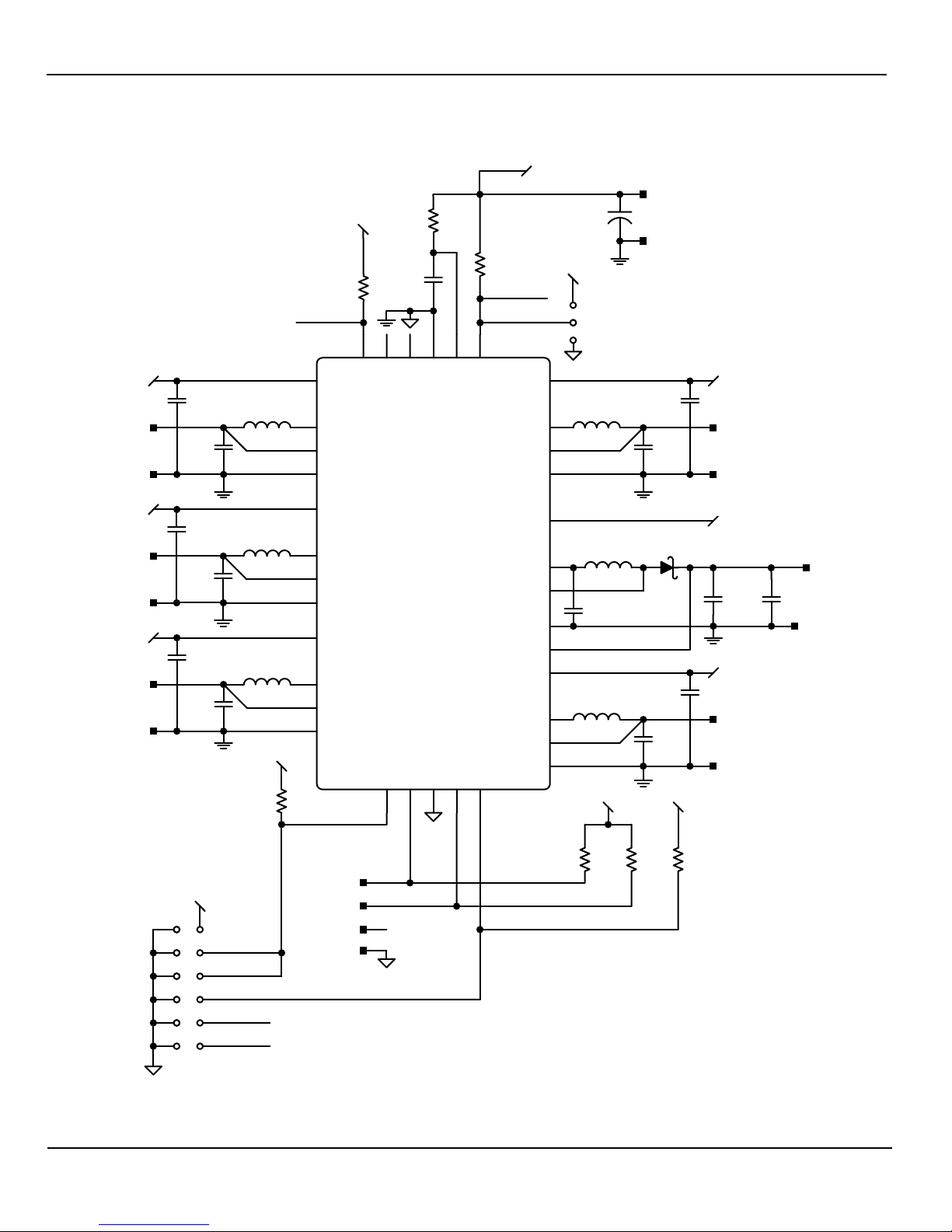
Evaluation Board Schematic
12
Revision 1.0
Page 13

Micrel, Inc.
MIC7401 Evaluation Board
July 21, 2015
(1)
(3)
Bill of Materials
Item Part Number Manufacturer Description Qty.
C1 CL05A225KO5NQNC Samsung
C2, C7, C9, C11,
C13
CL10A106MO8NQNC Samsung 10µF/16V, Ceramic, X5R, 0603, 0.8mm, ±20% 5
C4, C6 CL21A106KAYNNNE Samsung 10µF/25V, Ceramic, X5R, 0805, 1.25mm, ±20% 2
C3, C5, C8, C10,
C12, C14
C15 EEF-CX0J151XR
CL10A226MQ8NUNE Samsung 22µF/6.3V, Ceramic, X5R, 0603, 0.8mm, ±20% 6
Panasonic
D1 PMEG4002EL NXP
R1, R2 RC1005F104CS Samsung 100kΩ, Resistor, 0402, 1% 3
R3, R5 RC1005F202CS Samsung 2.0kΩ, Resistor, 0402, 1% 2
R4, R6 RC1005F4993CS Samsung 499kΩ, Resistor, 0402, 1% 1
R7 RC1005J000CS Samsung 0.00Ω, Resistor, 0402, Jumper 1
L1, L2, L3, L5, L6 CIG22H2R2MNE Samsung
L4 CIGW252010GM1R0MNE Samsung
U1 MIC7401YFL Micrel
Notes:
1. Samsung: www.samsung.com
2. Panasonic: www.panasonic.com.
3. NXP: www.nxp.com.
4. Micrel, Inc.: www.micrel.com.
.
2.2µF/16V, Ceramic, X5R, 0402, 0.8mm, ±10% 1
(2)
150µF/6.3V, POS Capacitor, SP, ±20% 1
0.2A/40V, Schottky, SOD-882 1
2.2µH, 1.6A Inductor, 116mΩ,
2520 × 1.2mm (maximum)
1.0µH, 3.3A Inductor
,
40mΩ,
2520 × 1.0mm (maximum)
(4)
Five-Channel Buck Regulator Plus One Boost
with HyperLight Load and I
2
C Control
5
1
1
13
Revision 1.0
Page 14
Micrel, Inc.
MIC7401 Evaluation Board
July 21, 2015
PCB Layout Recommendations
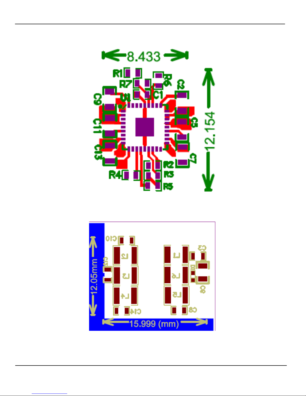
Evaluation Board Top Layer − Power Component Placement
Evaluation Board Top Layer − Layer 1 (Power Routing Layer)
14
Revision 1.0
Page 15
Micrel, Inc.
MIC7401 Evaluation Board
July 21, 2015
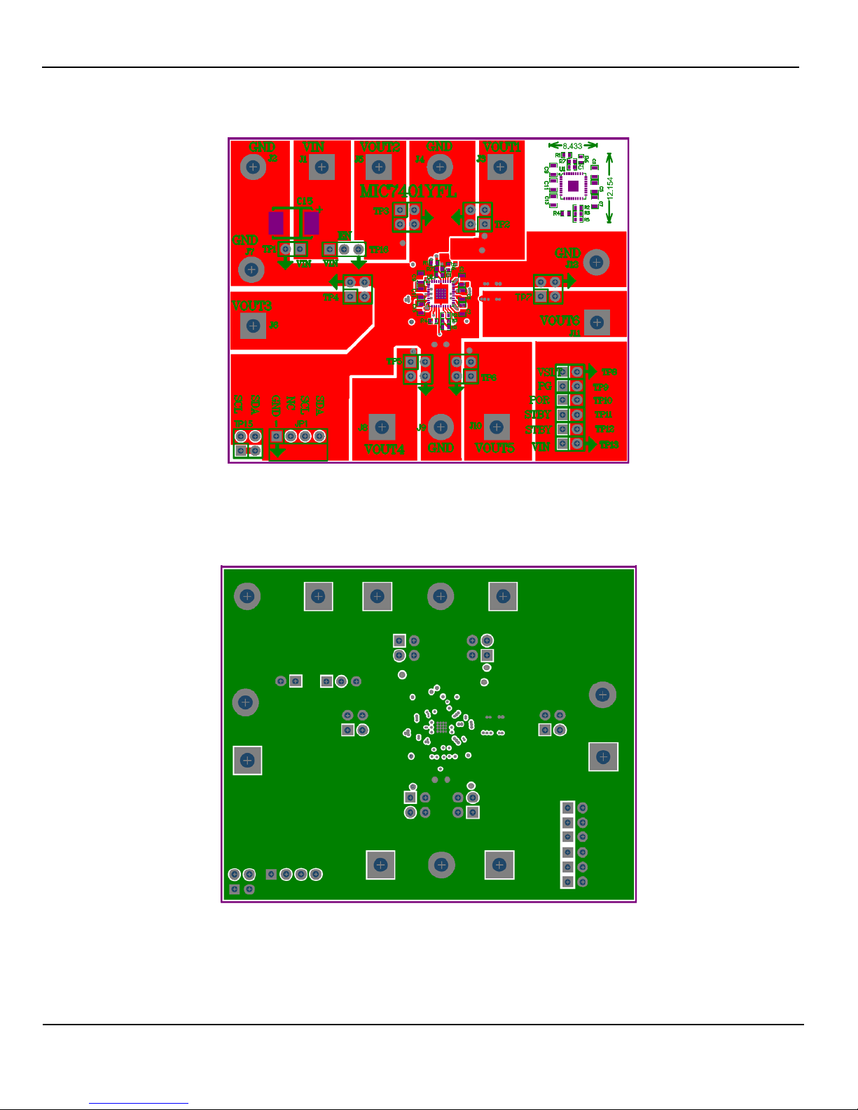
PCB Layout Recommendations (Continued)
Evaluation Board Top Layer − Layer 1 (Power Routing Layer)
Evaluation Board Layer 2 (Ground Plane)
15
Revision 1.0
Page 16
Micrel, Inc.
MIC7401 Evaluation Board
July 21, 2015
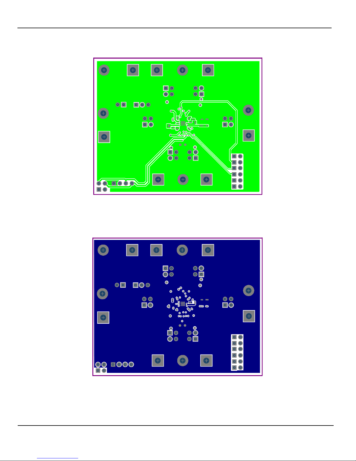
PCB Layout Recommendations (Continued)
Evaluation Board Top Layer − Layer 3 (Signal Routing Layer)
Evaluation Board Layer 4 (Ground Plane)
16
Revision 1.0
Page 17
Micrel, Inc.
MIC7401 Evaluation Board
July 21, 2015
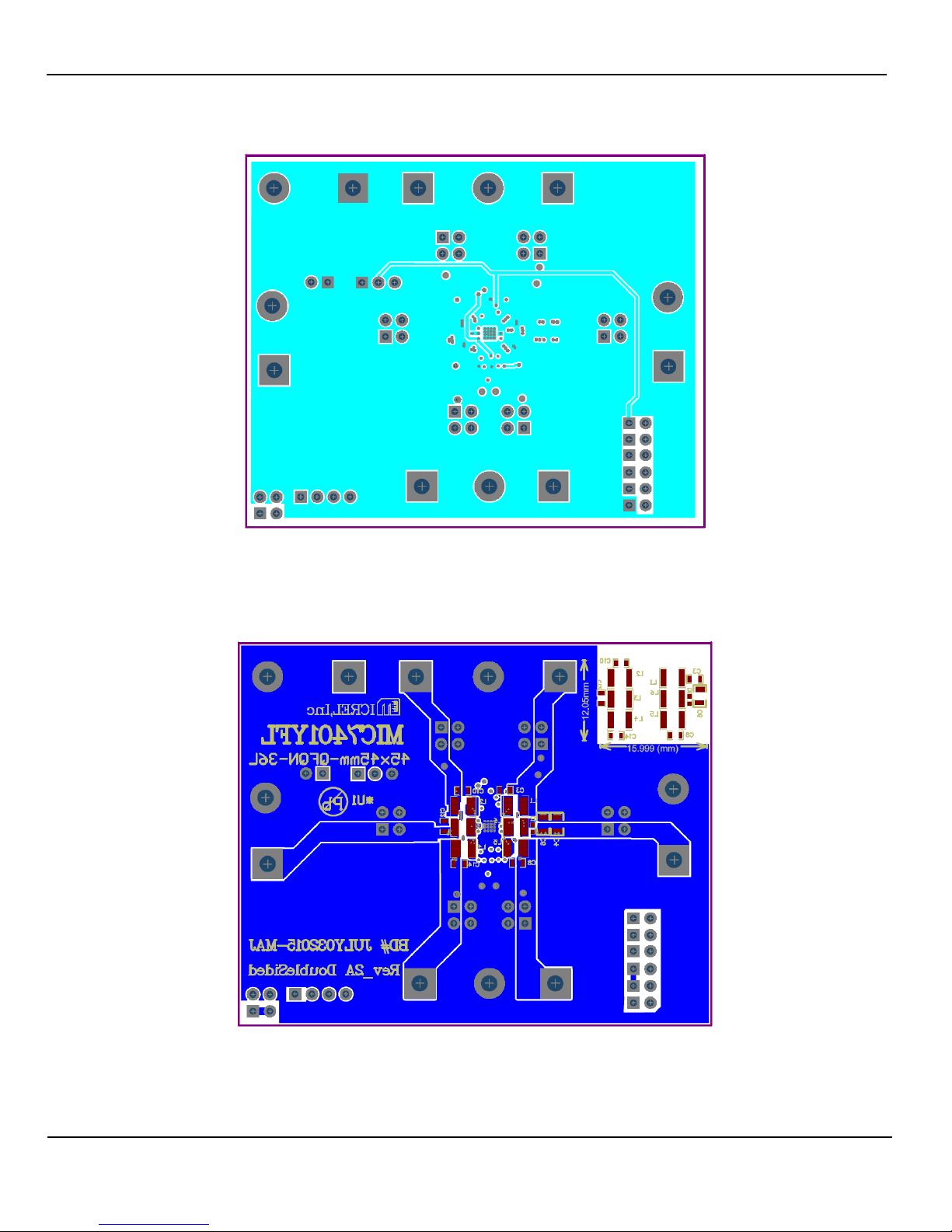
PCB Layout Recommendations (Continued)
Evaluation Board Layer − Layer 5 (VIN Plane)
Evaluation Board Bottom Later − Layer 6 (Ground Plane)
17
Revision 1.0
Page 18

Micrel, Inc.
MIC7401 Evaluation Board
July 21, 2015
MICREL, INC. 2180 FORTUNE DRIVE SAN JOSE, CA 95131 USA
Micrel, Inc. is a leading global m anufacturer of IC sol utions for the worldwide high-performance linear and power, LA N, and timing & comm unications
markets. The Company’s
performance communication, clock
management,
Company
customer
Corporation headquarters and state
s and support offices and
advanced technology design centers situated throughout t he Americas, Europe, and Asia. Additionally, the Company maintains an extensive network
of distributors and reps worldwide.
Micrel makes no representations or warranties
sheet. This
information is not intended as a warranty and Micrel does not assume responsibility for its use. Micrel reserves the right to change circuitry,
specification
No license, whether express, implied, arising by estoppel or otherwise, to any intell ectual
property rights
oducts, Micrel assumes no liabili ty
whatsoever, and Micrel disclaims any express or implied warranty relati ng to the sale and/or use of Micrel products including liability or warranties
relating to fitness for a particular purpose, merchantability, or infr
Micrel Products are not designed or authorized for use as com ponents in life support appliances, devices or systems where malf unction of a product
can reasonably be expected to result in personal injury. Life support devices or syst ems are devices or systems that (a) are intended for surgical
implant into the body or (b) support or sustain life, and whose fai l ure to perform can be reasonably expected to result in a
to the user. A
Purchaser’s use or sale of Micrel Products for use in life support appliances, devices or systems is a Purchaser’s own risk and P urchaser agrees t o fully
indemnify Micrel for any damages resulting from such use or sale.
TEL +1 (408) 944-0800 FAX +1 (408) 474-1000 WEB http://www.micrel.com
MEMs-based clock oscillators & crystal-less clock generators, Ethernet switches, and physical layer transceiver ICs.
s include leading manufacturers of enterprise, consumer, industrial, mobile, telecommunications, automotive, and computer products.
s and descriptions at any time without notice.
is grant ed by this document. E xcept as provided in Micrel’s terms and conditions of sale f or such pr
products include advanced mixed-signal, analog & power semiconductors; high-
-of-the-art wafer fabrication facilities are located in San Jose, CA, with regional sale
with respect to the accuracy or completeness of the information furnished in this data
ingement of any patent, copyright, or other intellectual property right.
© 2015 Micrel, Incorporated.
18
significant injury
Revision 1.0
Page 19

Mouser Electronics
Authorized Distributor
Click to View Pricing, Inventory, Delivery & Lifecycle Information:
Microchip:
ADM00812
 Loading...