

MIC74 Evaluation Board Micrel
MIC74 Evaluation Board
SMBus™ I/O Expander and Fan Controller Evaluation Board
General Description
This evaluation board demonstrates use of the MIC74 Serial
I/O expander and fan controller. It is designed to support rapid
prototyping of circuits employing the MIC74 as an I/O expander and/or a fan speed controller. Support is included for
dual power supplies in order to demonstrate the 5V-tolerant
I/O capabilities of the MIC74. An MIC5205 150mA LDO
regulator can be configured to supply 3.3V to the MIC74 while
the other circuitry is supplied from a single external 5V supply.
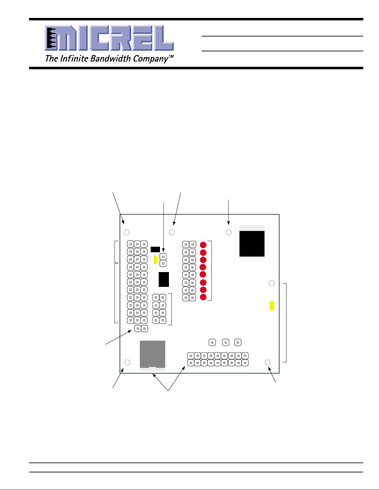
JP20
JP20
+2.7 - 3.3V
Input
MIC74BSM-16
J2
VDD
/SHDN
/FS0
Fan mode
/FS1
jumpers
/FS2
JP23 - JP26
Slave address
jumpers
JP17 - JP19
Input jumpers
JP1 - JP8
JP21
+5V
Input
A0
A1
A2
I0
I1
I2
I3
I4
I5
I6
I7
JP21
J5
GND
J1
5V
User configurable jumpers allow each of the MIC74’s I/O lines
to be used as an input or output, or the high-order lines can
be configured for fan speed control. An MIC29152, a highcurrent low-dropout regulator, is included to drive common
12V brushless DC fans.
A 4-pin connector is provided to interface the evaluation
board with a serial bus host such as the IPort™, an I2C™ Host
Adapter from MCC Corp. This connector is commonly used
for interoperability testing among SMBus™ or ACCESS.bus
hosts and peripherals. For more information regarding the
IPort™ I2C™ Host Adapter and the I2C™ Message Manager™ Software, see Appendix A.
Fan
supply
terminal
J3
LED0
LED7
07
JP22
12V
Output
jumpers
JP9 - JP16
& LEDs
TP1
TP2
(DATA)
(CLOCK)
TP1 TP2 TP3
TP3
(/ALERT)
MIC
29152BU
0000 X
U1
J6
GND
J4
VOUT
+
Fan
terminals
-
JP22
Ground
Ground
CON1
Host connections
MIC74 Evaluation Board Jumper and Connector Layout
SMBus™ is a trademark of Intel Corporation.
I2C™ is a trademark of Philips Electronics, N.V.
IPort™ and Message Manager™ are trademarks of Microcomputer Control Corporation.
Micrel, Inc. • 1849 Fortune Drive • San Jose, CA 95131 • USA • tel + 1 (408) 944-0800 • fax + 1 (408) 944-0970 • http://www.micrel.com
August 2000 1 MIC74
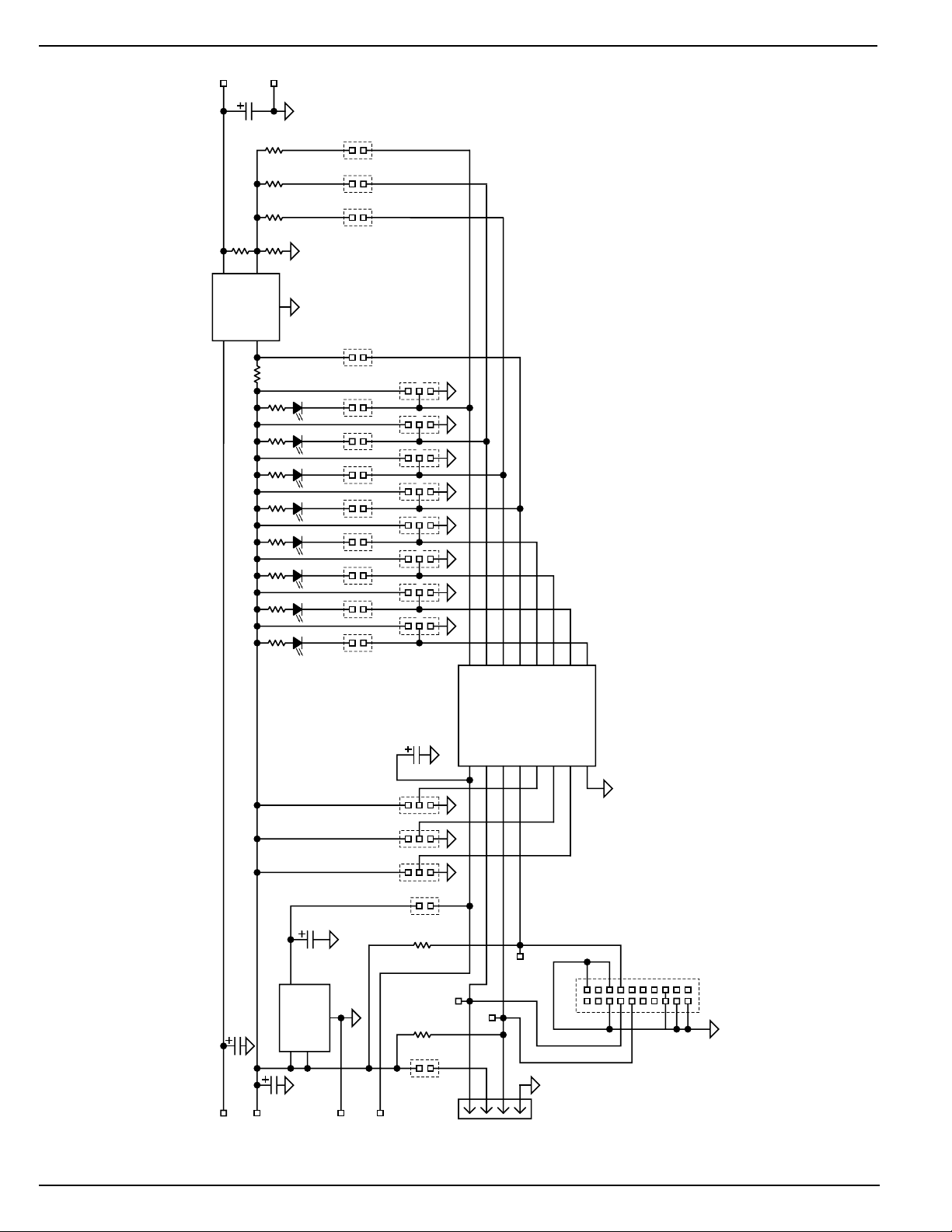
MIC74 Evaluation Board Micrel
IN
EN
GND
OUT
BYP
P7/FS2
P6/FS1
P3
P2
P1
P0
P5/FS0
P4/SHDN
MIC5205-3.3BM5
IN
EN
GND
OUT
FB
MIC29152BU
VDD
CLK
DATA
/ALERT
A2
A1
A0
GND
R10
3.3k
R
FB
3.01k
R
MIN
1k
R
F0
3.6k
R
F1
1.8k
RF21k
R2–R9 1kΩ
C3
22µF
20V
U1 MIC74BMM
4
6
8
10
12
14
16
18
20
123
12
12
21
2
1
1
3
13
13
13
13
13
13
13
21
21
21
21
21
21
21
3
21
5
7
9
11
13
15
17
19
TP2
JP22
Molex
TP1
TP3
JP21
JP20
JP17
JP18
JP1
A0
A1
JP19
A2
IN0
JP9
OUT0
OUT1
OUT2
OUT3
OUT4
OUT5
OUT6
OUT7
JP10
JP11
JP12
LED0
R9
LED1
R8
LED2
R7
LED3
R6
LED4
R5
LED5
R4
LED6
R3
LED7
R2
JP13
JP14
JP15
JP16
/SHDN
JP23
JP2
IN1
JP3
IN2
JP4
IN3
JP5
IN4
JP6
IN5
JP7
IN6
JP8
IN7
SMB_C
+5V
SMB_D
GND
C4
2.2µF
10V
J1
+5V
J4
VOUT
J6
GND
J3
+12V
J5
GND
R16
1.8k
J2
VDD
16 12
14 11
15 10
13 9
37
26
15
84
R1
10k
C5
0.01µF
C2
0.01µF
C1
0.01µF
CON1
2
2
2
2
2
2
2
2
4
5
3
1
2
21
/FS0
JP26
21
/FS1
JP25
21
/FS2
JP24
123
123
4
3
2
1
Figure 1. Evaluation Board Schematic
MIC74 2 August 2000
MIC74 Evaluation Board Micrel
Getting Started
What’s Included
Review the packing list in Table 1 to confirm that you received
all listed items. If any of the items are missing or damaged,
contact Micrel Semiconductor. The absolute latest version of
all Micrel device datasheets may be obtained from our
website at www.micrel.com.
metIytQnoitpircseD
11
21 launaMs'resUdraoBnoitaulavE47CIM
31 teehSataD47CIM
42 selpmaSSQB47CIM
51 teehSataD25192CIM
62 selpmaSUB25192CIM
71 teehSataD5025CIM
82 selpmaS5MB3.3-5025CIM
Table 1. Packing List
What You Must Provide
The following items are required for use with the MIC74
Evaluation Board:
• 5V, 100mA regulated power supply
• Power supply leads or cables
• SMBus/I2C compatible serial bus host for com-
munication with the MIC74
• Cable for serial host connection
• 12V-power supply rated to deliver the required
fan current*
• 12V brushless DC fan rated at no more than 1.5A
maximum*
* Required only for fan control applications
The following additional items are useful, but not required:
• Logic probe(s)
• Voltmeter(s)
• SMBus/I2C bus analyzer
htiwdraoBnoitaulavE47CIM
dellatsnIsrepmuJ
Powering the Board
The MIC74 evaluation board supports the use of dual power
supplies in order to demonstrate and make use of the
MIC74’s voltage-tolerant I/O capability. The LED indicators
can be powered from a 5V supply while the MIC74 is powered
from a lower voltage (2.7 to 3.6V). The MIC29152 linear
regulator in the optional fan control section requires a third,
higher voltage power supply. Three options are available for
powering the digital section of the evaluation board. Note that
in all cases, the pull-up resistors on /ALERT and the serial
data line are connected to the supply voltage present at J1.
Option 1
powering the board from a single 5V power supply connected
to J1 when a shorting block is installed at location JP20. The
MIC5205 generates the lower voltage (3.3V) required by the
MIC74 and feeds its VDD input via JP20. The LED’s indicators
on the board are powered from the 5V supply connected to
J1. JP21 should be removed or the 5V supply will be fed to pin
3 of the serial bus connector, CON1. Note that the pull-up
resistors on /ALERT and the serial data line are connected to
the supply voltage present at J1. The 3.3V output of U2 will
be present at J2.
Option 2
5V power supply connected to pin 3 when a shorting block is
installed at locations JP20 and JP21. The MIC5205 generates the lower voltage (3.3V) required by the MIC74 and
feeds its VDD input via JP20. The supply voltage applied at
CON1 will also be present at J1. The LED’s indicators on the
board are powered from the 5V supply connected to CON1.
The pull-up resistors on /ALERT and the serial data line are
connected to the supply voltage present at pin 3 of CON1.
The 3.3V output of U2 will be present at J2.
Option 3
power the entire evaluation board via J1 and J2. J1 and J2
should be connected together and JP20 is removed. This
isolates the MIC5205 from the circuit and ties both sections
together. The LED indicators will be powered from the same
supply as the MIC74. JP21 should be removed or the supply
voltage will be fed to pin 3 of the serial bus connector, CON1.
Note that the pull-up resistors on /ALERT and the serial data
line are connected to the supply voltage present at J1.
These options are summarized in Table 2. For each case, the
terminal used as the power supply input is highlighted in bold.
: An MIC5205-3.3BM5 linear regulator, U2, permits
: The board can be powered via CON1 by a single
: A single power supply between 2.7V and 3.6V can
noitpircseDnoitpO1J2J3:1NOC02PJ12PJ
;1JaivyppusV5elgniS
3:1NOCotdefylppus
;1JaivyppusV5elgniS
3:1NOCotdeftonylppus
1NOCaivyppusV5elgniStneserPV5tneserPV3.3 tupnIylppuSV5 detrohSdetrohS
;ylppusV3.3ot7.2elgniS
3:1NOCotdefylppus
;ylppusV3.3ot7.2elgniS
3:1NOCotdeftonylppus
tupnIylppuSV5 tneserPV3.3tneserPV5detrohSdetrohS
tupnIylppuSV5 tneserPV3.3nepOdetrohSnepO
tupnIylppuSV3 1JottcennoC
tupnIylppuSV3 1JottcennoCnepOnepOnepO
egatloVylppuS
tneserP
nepOdetrohS
Table 2. Options for Powering the Evaluation Board
August 2000 3 MIC74
MIC74 Evaluation Board Micrel
For fan control applications, an additional power supply is
connected to J3. This is nominally a 12V supply, but may be
higher, limited only by the MIC29152’s maximum input voltage of 26V.
Care must be taken, however, to insure that the
maximum power dissipation of the regulator is not exceeded.
If the regulator overheats, its internal thermal shutdown
circuitry will deactivate it. See MIC29152 datasheet.
Any of
the power supply arrangements listed in Table 2 may be used
in conjunction with a fan power supply at J3.
Serial Bus Host
The connector provided for the serial bus host is a Molex part
number 15-83-0064, 4-conductor shielded receptacle. The
pinout of this connector is shown below. The mating connector is Molex part number 15-83-1564. See Appendix A for
more information on these connectors. The serial bus signals
are also present on dual-row header JP22 and at test points
TP1 and TP2. One or more of these connection points can be
used in lieu of the specialized connector. The various serial
bus connection points are summarized in Table 3 below.
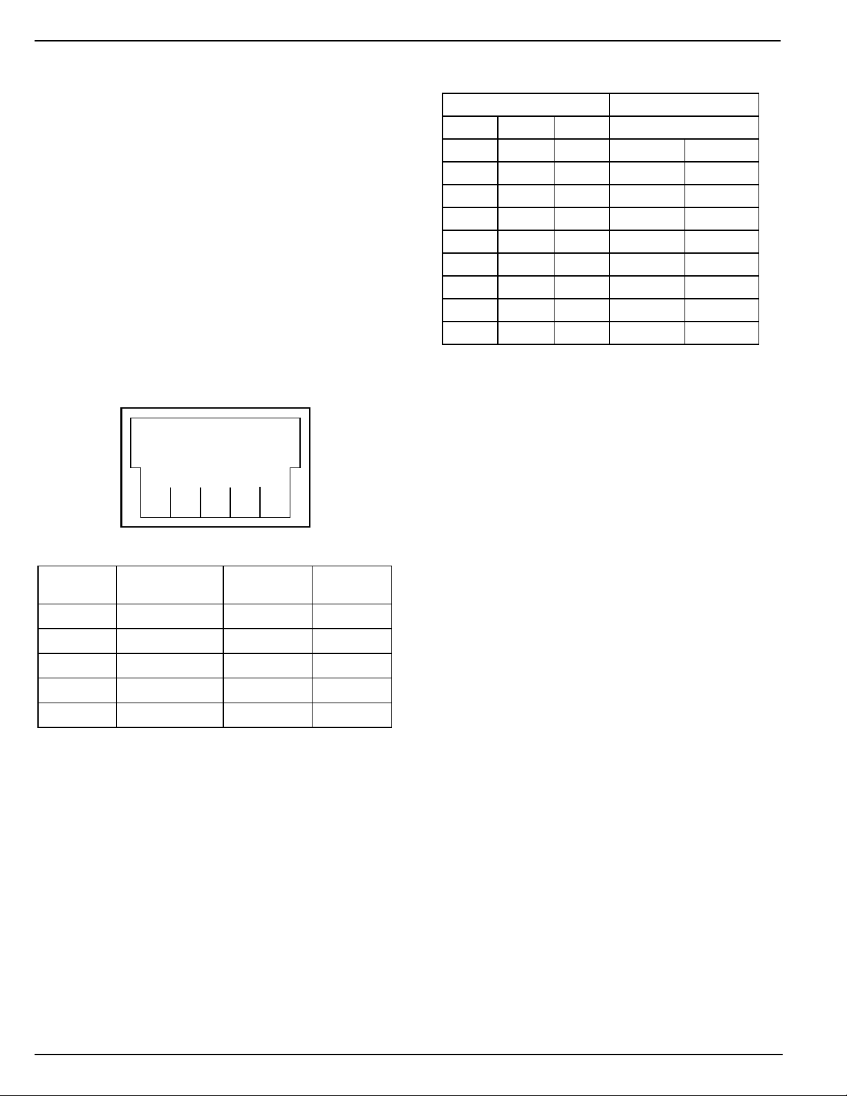
FRONT
CLK +5V DATA GND
4321
Molex 15-83-0064
There are eight possible slave addressess. Table 4 shows
each of the jumper settings and resulting slave addresses.
sgnitteSrepmuJsserddAevalS47CIM
91PJ81PJ71PJ
2A0A1A yraniBxeH
DNGDNGDNG0010 000
DNGDNGV50010 100
DNGV5DNG0010 010
DNGV5V50010 110
V5DNGDNG0010 001
V5DNGV50010 101
V5V5DNG0010 011
V5V5V50010 111
b
b
b
b
b
b
b
b
02
h
12
h
22
h
32
h
42
h
52
h
62
h
72
h
Table 4. Selecting the MIC74 Slave Address
Pull-up Resistors
The MIC74 evaluation board includes a pull-up resistor on the
serial data line and the MIC74’s /ALERT output, resistors R16
and R1, respectively. The serial clock line also requires a pullup resistor or current source somewhere in the system. If the
host does not have a provision for this pull-up, a pull-up
resistor will have to be added somewhere on the board, such
as between TP2 and J1. Guidelines for sizing this pull-up
resistor can be found in the SMBus specification.
in Appendix A.
See source
langiS
ataDlaireS291PT
kcolClaireS472PT
V5+3 a/na/n
DNG1 91,71,51,6,5,26J,5J
TRELA/a/n83PT
xeloM
#niP4600-38-51
#niP22PJtnioPtseT
Table 3. Serial Bus Connection Points
Personal computer based host adapters, cables, bus analyzers and other useful items can be obtained from the sources
listed in
Appendix A
.
Slave Address Selection
Before communication between the serial bus host and the
MIC74 can take place, the MIC74’s slave address must be
established. Jumpers JP17-19, marked “A0”, “A1”, and “A2”
on the PCB establish the slave address by connecting the A0,
A1, and A2 pins to 5V or ground. The address of the MIC74
is only registered at power-on and cannot be changed during
operation. To change the MIC74’s slave address, power
must be removed and then reapplied once the new settings
of JP17-19 have been established. The factory setting for the
MIC74’s slave address is 010 0000b (JP17 = JP18 = JP19 =
GND).
Checkout
Proper operation of all of the MIC74’s various functions can
be demonstrated and tested by a series of short exercises.
Each I/O pin is tested in its output mode and its input mode,
including the generation of interrupts. Lastly, the MIC74’s fan
mode operation is verified. If fan mode operation is not
desired, this section can be skipped.
Input Mode
The following steps will configure all I/O pins as inputs and
verify that the MIC74 is detecting and passing valid data.
1. Verify that jumpers JP1 - JP8 are adjusted so
that all MIC74 inputs will be grounded.
Figure 2.
2. Verify that the address selection jumpers are set
to match the slave address that will be used by
the host to communicate with the MIC74.
3. Apply power to the MIC74 evaluation board.
The MIC74 will be initialized to its default state,
all I/Os will be configured as inputs.
4. Read the data register, DATA. The value
returned should be 00h = 0000 0000b.
5. Connect any one of the input pins to 5V by
moving one of jumpers JP1-JP8. For example,
move JP3 to connect input I3 to 5V (logic high).
6. Read the data register, DATA. The value
returned should be 08h = 0000 1000b.
See
MIC74 4 August 2000

MIC74 Evaluation Board Micrel
7. Repeat steps 5 through 6 for each input in turn.
8. Confirm that the correct values were returned.
The following additional steps will verify that interrupts are
operating properly:
9. Configure jumpers JP1 - JP8 so that all inputs
are low.
10. Clear any pending interrupts by reading
STATUS
11. Enable interrupts by setting the interrupt enable
bit, IE, in the configuration register.
12. Enable interrupts on all inputs by setting all bits
in the interrupt mask register.
13. Connect a logic probe or voltmeter to TP3 to
monitor the /ALERT output. /ALERT should be
in its high state.
14. Read DATA. The data returned should be
0000 0000b.
A0
A1
A2
I0
I1
I2
I3
I4
I5
I6
I7
J1
+5V
JP19
JP18
JP17
JP1
JP2
JP3
JP4
JP5
JP6
JP7
JP8
U2
C4
MIC5205
JP20
MIC74
U3
/SHDN
/FS0
/FS1
/FS2
J2
VDD
C1
O0
O1
O2
O3
O4
O5
O6
O7
15. Connect any of the input pins to 5V by moving
one of JP1 - JP8. For example, move JP4 to
connect input I3 to 5V (logic high).
16. Confirm that /ALERT goes low and remains low
indefinitely.
17. Clear the interrupt by reading STATUS. The
value returned should match the input pattern.
(For example: 08h = 0000 1000b)
18. Verify that /ALERT returns high
19. Read DATA and verify that the value returned
matches the input data. (For example: 0000
1000b)
20. Repeat steps 15 through 19 for each input in
turn.
21. Remove all power from the MIC74 evaluation
board. Wait a few seconds for C4 to discharge.
J3
LED0
LED7
12V
R9
R8
R7
R6
R5
R4
R3
R2
C2
MIC29152BU
R10
RMIN
RFB
RF2
RF1
RF0
R1
U1
J4
VOUT
C3
J5
GND
JP21
R16
Connector
Molex
JP22
TP1
TP2
TP3
1
J6
GND
71565
2
Figure 2. Input Configuration
August 2000 5 MIC74

MIC74 Evaluation Board Micrel
Output Mode
The following steps will configure all I/O pins as outputs and
verify that the MIC74 is passing valid data.
1. Completely remove the jumpers from JP1 to JP8
and connect them to JP9 - JP16 to configure all
I/Os to drive the LED’s. See Figure 3 below.
2. Apply power to the board. The MIC74 will be
initialized to its power-up state.
3. Verify that all the LEDs are off at this point.
4. Configure all I/Os as outputs by setting all bits in
the data direction register, i.e., write DIR with
FFh.
J1
+5V
A0
A1
A2
I0
I1
I2
I3
I4
I5
I6
I7
U2
C4
MIC5205
JP20
MIC74
U3
/SHDN
/FS0
/FS1
/FS2
J2
VDD
C1
O0
O1
O2
O3
O4
O5
O6
JP9
JP10
JP11
JP12
JP13
JP14
JP15
JP16
O7
5. Set all I/Os to their high (open-drain) state by
setting all bits in DATA, i.e., write DATA with
FFh
6. Verify that all the LEDs are off at this point.
7. Clear any bit in the data register. For example,
write DATA with F7h = 1111 0111b to clear
output #3.
8. Verify that LED #3 turns on and all other LED’s
are off.
9. Repeat steps 7 and 8 for each output bit.
10. Remove all power from the MIC74 evaluation
board. Wait a few seconds for C4 to discharge.
J3
LED0
LED7
12V
R9
R8
R7
R6
R5
R4
R3
R2
C2
MIC29152BU
R10
RMIN
RFB
RF2
RF1
RF0
R1
U1
J4
VOUT
C3
J5
GND
JP21
R16
Molex
JP22
Connector
71565
Figure 3. Output Configuration
TP1
TP2
TP3
1
J6
GND
2
MIC74 6 August 2000

MIC74 Evaluation Board Micrel
Fan Mode
The following steps will configure the board for fan speed
control and verify proper operation.
1. Remove the eight jumpers from JP1 - JP8 and
use four of the jumpers to short JP23 - JP26.
See Figure 4 below.
2. Connect the positive lead of the 12V fan to J4
(MIC29152’s output) and the negative wire of
the 12V fan to J6 (Ground).
3. Apply power to the board. The MIC74 will be
initialized to its power-up state. See the
datasheet Applications section.
4. Connect the 12V power supply to the
MIC29152’s input at J3.
5. Verify that the fan comes on at its minimum
speed. (It will remain in this state while the
MIC74 is programmed for fan mode.)
J1
+5V
A0
A1
A2
I0
I1
I2
I3
I4
I5
I6
I7
U2
C4
MIC5205
JP20
MIC74
U3
JP23
JP26
JP25
JP24
J2
VDD
C1
/SHDN
/FS0
/FS1
/FS2
O0
O1
O2
O3
O4
O5
O6
O7
6. Enable fan mode by setting the fan bit in
DEV_CFG, i.e., write DEV_CFG with 02h.
7. Select the desired speed by writing to
FAN_SPEED. (Table 3 shows the output
voltage for the seven available speeds.)
8. Verify by observation that the fan speed
changes.
9. Verify that the output voltage of the MIC29152 is
close to the value given in Table 3 (This voltage
will vary slightly due to resistor tolerances,
component accuracy, etc.)
10. Repeat steps six and seven for each possible
fan speed value.
11. Remove all power from the MIC74 evaluation
board. Wait a few seconds for C4 to discharge.
J3
LED0
LED7
12V
R9
R8
R7
R6
R5
R4
R3
R2
C2
MIC29152BU
R10
RMIN
RFB
RF2
RF1
RF0
R1
U1
J4
VOUT
C3
J5
GND
JP21
R16
Connector
Molex
JP22
TP1
TP2
TP3
1
J6
GND
71565
2
Figure 4. Fan Configuration
August 2000 7 MIC74

MIC74 Evaluation Board Micrel
Table 5 lists the fan speed and MIC29152 output voltage
produced by a given value written into FAN_SPEED. The
actual measured voltage may vary slightly from the values
shown in the table due to resistor tolerances, component
accuracy, etc. R
in the table is the equivalent feedback
EQ
DEEPS_NAF
eulaV
00000000
b
00000000
b
10000000
b
01000000
b
11000000
b
00100000
b
10100000
b
01100000
b
11100000
b
deepSnaF
R
detceleS
BF
pu-rewopk3k1neponeponepok1V69.4
ffonafk3k1neponeponepok1V0
tsewolk3k1neponepok6.3387V99.5
tsewoldn2k3k1nepok8.1nepo346V30.7
tsewoldr3k3k1nepok8.1k6.3545V60.8
muidemk3k1k1neponepo005V86.8
tsehgihdr3k3k1k1nepok6.3934V17.9
tsehgihdn2k3k1k1k8.1nepo193V57.01
tsehgihk3k1k1k8.1k6.3353V87.11
R
NIM
Table 5. Fan Drive Voltages vs. Value in FAN_SPEED
resistance that results from the parallel combination of RF0,
RF1, RF2, R
, as applicable for each speed setting. Refer
MIN
to the Applications section of the MIC74 datasheet for a
detailed explanation of fan mode and how to select resistors
for a given application.
R
2F
R
1F
R
0F
R
QE
V
TUO
Hardware Reference
rotangiseDnoitpircseD
1JtupnIylppuSrewoPV5
2JVs'47CIM
3JtupnIylppuSrewoPV21
4JV25192CIM(egatloVevirDnaF
5JdnuorG
6JdnuorG
tupnI
DD
)
TUO
Table 6. Terminals
MIC74 8 August 2000
rotangiseDnoitpircseD
1PTATAD
2PTKCOLC
3PTTRELA/
Table 7. Test Points

MIC74 Evaluation Board Micrel
repmuJnoitisoPnoitcnuF
1PJ
2PJ
3PJ
4PJ
5PJ
6PJ
7PJ
8PJ
9PJ2ot1edomtuptuoniard-neponi0Pot0DELtcennoCnepO
01PJ2ot1edomtuptuoniard-neponi1Pot1DELtcennoCnepO
11PJ2ot1edomtuptuoniard-neponi2Pot2DELtcennoCnepO
21PJ2ot1edomtuptuoniard-neponi3Pot3DELtcennoCnepO
31PJ2ot1edomtuptuoniard-neponi4Pot4DELtcennoCnepO
41PJ2ot1edomtuptuoniard-neponi5Pot5DELtcennoCnepO
51PJ2ot1edomtuptuoniard-neponi6Pot6DELtcennoCnepO
61PJ2ot1edomtuptuoniard-neponi7Pot7DELtcennoCnepO
71PJ
81PJ
91PJ
02PJ2ot147CIMehtotV3.3edivorPnepO
12PJ2ot1rotcennoCxeloMehtmorfV5esUnepO
32PJ2ot1edomnafninipNDHS/otnipelbanes'25192CIMtcennoCnepO
42PJ2ot1edomnafninip2SF/ot2FRtcennoCnepO
52PJ2ot1edomnafninip1SF/ot1FRtcennoCnepO
62PJ2ot1edomnafninip0SF/ot0FRtcennoCnepO
2ot1
3ot2
2ot1
3ot2
2ot1
3ot2
2ot1
3ot2
2ot1
3ot2
2ot1
3ot2
2ot1
3ot2
2ot1
3ot2
2ot1
3ot2
2ot1
3ot2
2ot1
3ot2
V5ot0AtcennoC
dnuorGot0AtcennoC
V5ot1AtcennoC
dnuorGot1AtcennoC
V5ot2AtcennoC
dnuorGot2AtcennoC
edomtupniehtnidnuorGot0PtcennoC
edomtupniehtniV5ot0PtcennoC
edomtupniehtnidnuorGot1PtcennoC
edomtupniehtniV5ot1PtcennoC
edomtupniehtnidnuorGot2PtcennoC
edomtupniehtniV5ot2PtcennoC
edomtupniehtnidnuorGot3PtcennoC
edomtupniehtniV5ot3PtcennoC
edomtupniehtnidnuorGot4PtcennoC
edomtupniehtniV5ot4PtcennoC
edomtupniehtnidnuorGot5PtcennoC
edomtupniehtniV5ot5PtcennoC
edomtupniehtnidnuorGot6PtcennoC
edomtupniehtniV5ot6PtcennoC
edomtupniehtnidnuorGot7PtcennoC
edomtupniehtniV5ot7PtcennoC
yrotcaF
gnitteS
detrohS
nepO
detrohS
nepO
detrohS
nepO
detrohS
nepO
detrohS
nepO
detrohS
nepO
detrohS
nepO
detrohS
nepO
nepO
detrohS
nepO
detrohS
nepO
detrohS
Table 8. Jumper Options
August 2000 9 MIC74

MIC74 Evaluation Board Micrel
Printed Circuit Layouts
Top-Side Silk Screen
Bottom-Side Silk Screen
Top-Side Copper
MIC74 10 August 2000
Bottom-Side Copper

MIC74 Evaluation Board Micrel
Bill of Materials
Item Part Number Manufacturer Description Qty.
C1, C2, C5 08055C103MAT2 AVX 0.01µF 50V 3
C3 TPSC226M016R0375 AVX 22µF 16V 1
C4 TAJA225M010R AVX 2.2µF 10V 1
LED0–LED7 LTC-16KE Vishay Lite-On LED 8
R1 CRCW08051002FRT1 Vishay-Dale 10k ±1%, size 0805 or 1206 1
R10 CRCW08053301FRT1 Vishay-Dale 3.3k ±1%, size 0805 or 1206 1
R
F0
RF1, R16 CRCW08051801FRT1 Vishay-Dale 1.8k ±1%, size 0805 or 1206 2
R
, RF2, R2–R9 CRCW08051001FRT1 Vishay-Dale 1k ±1%, size 0805 or 1206 10
MIN
R
FB
U1 MIC29152-BU Micrel High-Current LDO Regulator 1
U2 MIC5205-3.3BM5 Micrel 150mA Low-Noise LDO Regulator 1
U3 MIC74BMM Micrel SMBus™ I/O Expander and Fan Controller 1
CON1 15-83-0064 Molex 4-position female connector 1
CRCW08053601FRT1 Vishay-Dale 3.6k ±1%, size 0805 or 1206 1
CRCW08053011FRT1 Vishay-Dale 3.01k ±1%, size 0805 or 1206 1
August 2000 11 MIC74

MIC74 Evaluation Board Micrel
Appendix A: SMBus Resources*
PC host adapters and software, bus analyzers, cables, and
other items can be purchased from:
Micro Computer Control Corporation
PO Box 275/ 17 Model Ave
Hopewell, New Jersey 08525 USA
Telephone: 609-466-1751
Email: info@mcc-us.com
http://www.mcc-us.com
The 4-conductor serial bus connector is available from Molex
as part number 15-83-0064. Mating plugs for constructing
cable assemblies are also available. A list of distributors is
available on the Molex website.
Molex Incorporated
2222 Wellington Court
Lisle, IL 60532-1682
Tel: 800/78MOLEX,
630/969-4550 (Outside USA)
Fax: 630/968-8356
Telex: 254069
E-mail: amerinfo@molex.com
http://www.molex.com
The current SMBus specification and other information regarding SMBus may be obtained from the SMBus website
SMBus Forum (website)
http://www.smbus.org.
*Micrel does not necessarily endorse or recommend any of
the products, services, or information sources listed above.
Micrel is not affiliated in any way with any listed company,
person, or other entity. The above information is presented
without warranty of any kind.
MICREL INC. 1849 FORTUNE DRIVE SAN JOSE, CA 95131 USA
TEL + 1 (408) 944-0800 FAX + 1 (408) 944-0970 WEB http://www.micrel.com
This information is believed to be accurate and reliable, however no responsibility is assumed by Micrel for its use nor for any infringement of patents or
other rights of third parties resulting from its use. No license is granted by implication or otherwise under any patent or patent right of Micrel Inc.
© 2000 Micrel Incorporated
MIC74 12 August 2000
 Loading...