

MIC7201 Micrel
MIC7201
GainBlock™ Difference Amplifier
Preliminary Information
General Description
The MIC7201 difference amplifier is an analog gain block
designed to convert a differential signal to a signal-ended
signal. It features an extended common-mode range that
includes rail-to-rail input/output capabilities. The part is packaged in the SOT-23-5 IttyBitty™ package.
The MIC7201 is designed using the MIC7101 operational
amplifier plus well-matched monolithic resistors to provide a
unity-gain stable differential input to signal-ended output
amplifier that requires a minimum of external components.
Performance is guaranteed from 2.2V through 10V.
Features
• Operates from 2.2V to 10V
• ±1% typical gain error
• 0.6mA typical supply current at 2.2V
• 400kHz bandwidth
• Small SOT-23-5 package
• Suitable for driving capacitive loads
Applications
• Cellular telephones
• Digital audio systems
• Mobile communications
• Portable computers and PDAs
Ordering Information
Part Number Temperature Range Package
MIC7201BM5 –40°C to +85°C SOT-23-5
Other voltages available. Contact Micrel for details.
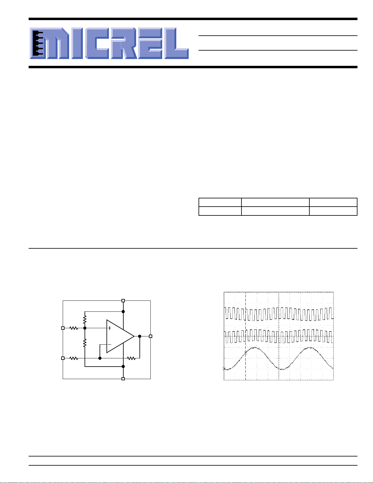
Block Diagram
IN+
IN–
50k
3
50k
4
MIC7201
100k
100k
V+
V–
2
V
IN–
OUT
1
50k
5
V
V
OUT
IN+
Difference Amplifier Behavior
The desired 100mV, 400Hz differential sinusoidal signal is shown applied to
inputs V
imposed on both V
These signals demonstrate the noise cancellation ability of the MIC7201.
The output (V
400Hz sine wave.
IN–
and V
. A 500mV, 5kHz square-wave “noise” signal is super-
IN+
and V
IN–
) shows the recovered single-ended 200mV peak-to-peak,
OUT
IN+
.
GainBlock is a trademark of Micrel, Inc.
Micrel, Inc. • 1849 Fortune Drive • San Jose, CA 95131 • USA • tel + 1 (408) 944-0800 • fax + 1 (408) 944-0970 • http://www.micrel.com
December 1998 1 MIC7201
MIC7201 Micrel
Pin Configuration
Pin Description
Pin Number Pin Name Pin Function
1 OUT Amplifier Output: Single-ended output.
2 V+ Positive Supply: Positive power supply input.
3 IN+ Noniverting Input: In-phase differential input.
4 IN– Inverting Input: Out-of-phase differential input.
5 V– Ground: Power supply ground return.
IN+
OUTV+
13
2
A16
45
IN–
SOT-23-5
V–
Part
Identification
MIC7201 2 December 1998
MIC7201 Micrel
Absolute Maximum Ratings (Note 1)
Supply Voltage (VV+–VV–).............................................12V
Differential Input Voltage (VV+–VV–) .................±(VV+–VV–)
I/O Pin Voltage (VIN, V
................................................ VV––0.3V to VV++0.3V
Junction Temperature (TJ) ...................................... +150°C
Storage Temperature (TS) ....................... –65°C to +150°C
Lead Temperature (soldering, 10 sec.) .....................260°C
OUT
), Note 2
Operating Ratings (Note 1)
Supply Voltage (VV+–VV–)............................ +2.2V to +10V
Input Voltage (V
Continuous Output Current ......................................±15mA
Junction Temperature (TJ) ......................... –40°C to +85°C
Max. Junction Temperature (T
Package Thermal Resistance (θJA), Note 4..........325°C/W
Max. Power Dissipation............................................ Note 3
IN+
, V
)................................... VV– to V
IN–
), Note 3 ...........+85°C
J(max)
ESD, Note 5.................................................................. 2kV
Electrical Characteristics (2.2V)
VV+ = 2.2V, VV– = 0V, VCM = V
Symbol Parameter Condition Min Typ Max Units
E
Z
TCV
R
IN
OS
Zero Error EZ = V
Input Offset Voltage Temp. Drift 14 µV/°C
Input Resistance 35 50 65 kΩ
CMRR Common-mode Rejection Ratio VCM = 0V to V
±PSRR Split-Supply Rejection Ratio V
+PSRR Single-Supply Rejection Ratio, V
Note 8
E
V
I
G
OUT
SC
Gain Error, Note 9 0.2V ≤ V
Output Voltage Swing output high, RL = 2k, 10 33 mV
Note 10 specified as VV+ – V
Output Short-Circuit Current sinking or sourcing, Note 6, Note 7 20 60 mA
BW Bandwidth –3dB point 400 kHz
SR Slew Rate 0.5 V/µs
THD Total Harmonic Distortion f = 1kHz 0.02 %
e
n
I
S
Input Referred Voltage Noise f = 1kHz 30
Supply Current no load 0.6 2.0 mA
= V+/2; RL = 1MΩ; TJ = 25°C, bold values indicate –40°C ≤ TJ ≤ +85°C; unless noted
OUT
– VV+/2 944mV
OUT
V+
= VV– = 1.1V to 2.5V, 50 dB
V+
VCM = 0V
= 2.2V to 5V, VV– = 0V, VCM = 1.1V 6 dB
V+
≤ 2.0V ±1%
OUT
OUT
output low, R
output high, R
specified as VV+ – V
output low, R
= 2k 10 33 mV
L
= 600Ω,33mV
L
OUT
= 600Ω 33 mV
L
f = 10kHz 0.02 %
65 dB
50 mV
50 mV
mV
mV
nV Hz/
V+
December 1998 3 MIC7201

MIC7201 Micrel
Electrical Characteristics (5V)
VV+ = +5V, VV– = 0V, VCM = V
Symbol Parameter Condition Min Typ Max Units
E
Z
TCV
R
IN
OS
Zero Error EZ = V
Input Offset Voltage Temp. Drift 14 µV/°C
Input Resistance 35 50 65 kΩ
CMRR Common-Mode Rejection Ratio VCM = 0V to V
±PSRR Split-Supply Rejection Ratio V
+PSRR Single-Supply Rejection Ratio, V
Note 8
E
V
G
OUT
Gain Error, Note 9 0.5V ≤ V
Output Voltage Swing output high, RL = 2k, 15 50 mV
Note 10 specified as VV+ – V
I
SC
Output Short-Circuit Current sinking or sourcing, Note 6, Note 7 40 110 mA
BW Bandwidth –3dB point 250 kHz
SR Slew Rate 0.5 V/µs
THD Total Harmonic Distortion f = 1kHz 0.02 %
e
n
I
S
Input Referred Voltage Noise f = 1kHz 30
Supply Current no load 0.8 2.8 mA
= V+/2; RL = 1MΩ; TJ = 25°C, bold values indicate –40°C ≤ TJ ≤ +85°C; unless noted
OUT
– VV+/2 26 100 mV
OUT
V+
= VV– = 2.5V to 5V, 50 dB
V+
VCM = 0V
= 5V to 10V, VV– = 0V, VCM = 2.5V 6 dB
V+
≤ 4.5V ±1%
OUT
OUT
output low, R
output high, R
specified as VV+ – V
output low, R
= 2k 15 50 mV
L
= 600Ω,50mV
L
OUT
= 600Ω 50 mV
L
f = 10kHz 0.02 %
65 dB
75 mV
75 mV
mV
mV
nV Hz/
Electrical Characteristics (10V)
VV+ = 10V, VV– = 0V, VCM = V
Symbol Parameter Condition Min Typ Max Units
E
Z
TCV
R
IN
OS
Zero Error EZ = V
Input Offset Voltage Temp. Drift 14 µV/°C
Input Resistance 35 50 65 kΩ
CMRR Common-Mode Rejection Ratio VCM = 0V to V
±PSRR Split-Supply Rejection Ratio V
+PSRR Single-Supply Rejection Ratio, V
Note 8
E
G
Gain Error, Note 9 0.5V ≤ V
= V+/2; RL = 1MΩ; TJ = 25°C, bold values indicate –40°C ≤ TJ ≤ +85°C; unless noted
OUT
– VV+/2 60 200 mV
OUT
V+
= VV– = 2.5V to 5V, 50 dB
V+
VCM = 0V
= 5V to 10V, VV– = 0V, VCM = 2.5V 6 dB
V+
≤ 9.5V ±1%
OUT
65 dB
MIC7201 4 December 1998

MIC7201 Micrel
Symbol Parameter Condition Min Typ Max Units
V
OUT
Output Voltage Swing output high, RL = 2k, 24 80 mV
Note 10 specified as VV+ – V
output low, R
= 2k 24 80 mV
L
OUT
120 mV
120 mV
output high, R
specified as VV+ – V
output low, R
I
SC
Output Short-Circuit Current sinking or sourcing, Note 6, Note 7 40 200 mA
= 600Ω,80mV
L
OUT
= 600Ω 80 mV
L
mV
mV
BW Bandwidth –3dB point 250 kHz
SR Slew Rate 0.5 V/µs
THD Total Harmonic Distortion f = 1kHz 0.02 %
f = 10kHz 0.02 %
e
n
I
S
Input Referred Voltage Noise f = 1kHz 30
nV Hz/
Supply Current no load 1.2 4.0 mA
Internal Op Amp Typical Characteristics
+2.2V ≤ VV+ ≤ 10V, VV– = 0V, VCM = V
Symbol Parameter Condition Min Typ Max Units
V
OS
TCV
I
B
I
OS
R
IN
OS
Input Offset Voltage 0.11 mV
Input Offset Voltage Drift 1.0 µV/°C
Input Bias Current 1.0 pA
Input Offset Current 0.5 pA
Input Resistance >1 TΩ
CMRR Common-Mode Rejection Ratio 0V ≤ VCM ≤ V
V
CM
Input Common-Mode Voltage input low –0.3 V
PSRR Power Supply Rejection Ratio V
= V+/2; RL = 1MΩ; TJ = 25°C, bold values indicate –40°C ≤ TJ ≤ +85°C; unless noted
OUT
V+
80 dB
input high VV++0.3 V
= VV– = 1.1V to 1.65V, 60 dB
V+
VCM = 0V
General Note: Devices are ESD protected; however, handling precautions are recommended. All limits guaranteed by testing or statistical analysis.
Note 1: Absolute maximum ratings indicate limits beyond which damage to the component may occur. Electrical specifications do not apply when
Note 2: I/O pin voltage is any external voltage to which an input or output is referenced.
Note 3: The maximum allowable power dissipation is a function of the maximum junction temperature, T
Note 4: Thermal resistance, θJA, applies to a part soldered on a printed-circuit board.
Note 5: Human body model, 1.5k in series with 100pF.
Note 6: Short circuit may cause the device to exceed maximum allowable power dissipation. See Note 3.
Note 7: Shorting V
Note 8: Limited by internal bias-network resistors. Power supply must be “clean.” Power supply should be bypassed as shown in typical application
Note 9: The gain error specification applies to differential, inverting, and noninverting gains.
Note 10: Since the part is specified in a single-supply configuration, the output load (RL) is a Thevenin equivalent value. The actual load consists of 2 ×
operating the device outside its recommended operating ratings.
; the junction-to-ambient thermal
resistance, θJA; and the ambient temperature, TA. The maximum allowable power dissipation at any ambient temperature is calculated using:
PD = (T
circuit.
RL to ground and 2 × RL to the supply (V+).
– TA) / θJA. Exceeding the maximum allowable power dissipation will result in excessive die temperature.
J(max)
to V+ when V+ > 10V may damage the device.
OUT
J(max)
December 1998 5 MIC7201

MIC7201 Micrel
IN+
OUT
50k
100k
V+
50k
50k
100k
IN–
V–
MIC7201
1
2
3
4
5
V
V+
0.1µF
V
V
2
OUT
V+
=
V
V+
V+
2
Applications Information
Input Common Mode Voltage
The MIC7201 tolerates overdriving the inputs by at least
300mV beyond either rail without producing phase inversion.
If the absolute maximum input voltage is exceeded, the input
current should be limited to ±5mA to prevent reducing reliability. A 10kΩ series input resistor, used as a current limiter will
protect the input structure from voltages as large as 50V
above the supply or below ground.
Output Voltage Swing
IN+
V
IN
3
IN–
4
50k
50k
MIC7201
100k
100k
V–
OUT
1
50k
5
V
IN
V
=
OUT
2
Output resistance of the MIC7201 is symmetric; sink and
source output resistances are equal. Output voltage swing is
determined by the load and, given the approximate output
resistance, which may be readily calculated with the following
formula:
V
≈
I
and I
DROP
LOAD
can be determined from the V
LOAD
OUT
R
OUT
V
is the voltage dropped within the amplifier output
DROP
stage. V
DROP
(output swing) portion of the appropriate Electrical Characteristics table. I
minus V+/2 and divided by R
is equal to the typical output high voltage
LOAD
. For example, using the
LOAD
Electrical Characteristics DC (5V) table, the typical output
voltage drop using a 2kΩ load (connected to V+/2) is 0.015V,
which produces an I
of (2.5V – 0.015V) / 2kΩ ≈ 1.243mA.
LOAD
Then:
R
OUT
15mV
==≈12 1 2. Ω
1.243mA
1
V
V
V+
2
Figure 2. Gain of One-Half
50k
50k
100k
100k
V–
IN+
IN
3
IN–
4
MIC7201
Figure 3. Voltage Follower
V+
V+
V
V+
2
OUT
V
= V
OUT
1
50k
5
V
V+
2
IN
Driving Capacitive Loads
Driving a capacitive load introduces phase-lag into the output
signal, and this in turn reduces system phase margin. The
application that is least forgiving of reduced phase margin is
a unity gain amplifier. The MIC7201 typically can drive a
500pF capacitive load connected directly to its output.
V
SUPPLY
0.1µF
IN+
3
IN–
V
IN
4
50k
50k
MIC7201
100k
100k
V–
OUT
V
= –V
OUT
1
50k
5
IN
Digital
Input
DAC
0.1µF
I
OUT
I
0.1µF
OUT
4.7µF
MIC7201
0.1µF
0.1µF
V
OUT
R
L
Figure 4. Inverting Unity Gain
Figure 1. Audio DAC
Figure 5. Virtual Ground Generator
MIC7201 6 December 1998

MIC7201 Micrel
Package Information
1.90 (0.075) REF
0.95 (0.037) REF
3.02 (0.119)
2.80 (0.110)
0.50 (0.020)
0.35 (0.014)
1.75 (0.069)
1.50 (0.059)
1.30 (0.051)
0.90 (0.035)
0.15 (0.006)
0.00 (0.000)
SOT-23-5 (M5)
3.00 (0.118)
2.60 (0.102)
10°
0°
DIMENSIONS:
MM (INCH)
0.20 (0.008)
0.09 (0.004)
0.60 (0.024)
0.10 (0.004)
December 1998 7 MIC7201

MIC7201 Micrel
MICREL INC. 1849 FORTUNE DRIVE SAN JOSE, CA 95131 USA
TEL + 1 (408) 944-0800 FAX + 1 (408) 944-0970 WEB http://www.micrel.com
This information is believed to be accurate and reliable, however no responsibility is assumed by Micrel for its use nor for any infringement of patents or
other rights of third parties resulting from its use. No license is granted by implication or otherwise under any patent or patent right of Micrel Inc.
© 1998 Micrel Incorporated
MIC7201 8 December 1998
 Loading...